Abstract
An approach to implement single-ended power-efficient static class-AB Miller op-amps with symmetrical and significantly enhanced slew-rate and accurately controlled output quiescent current is introduced. The proposed op-amp can drive a wide range of resistive and capacitive loads. The output positive and negative currents can be much higher than the total op-amp quiescent current. The enhanced performance is achieved by utilizing a simple low-power auxiliary amplifier with resistive local common-mode feedback that increases the quiescent power dissipation by less than 10%. The proposed class AB op-amp is characterized by significantly enhanced large-signal dynamic, static current efficiency, and small-signal figures of merits. The dynamic current efficiency is 15.6 higher, the static current efficiency is 10.6 times higher, and the small-signal figure of merit is 2.3 times higher than the conventional class-A op-amp. A global figure of merit that determines an op-amp’s ultimate speed is 6.33 times higher than the conventional class A op-amp.
1. Introduction
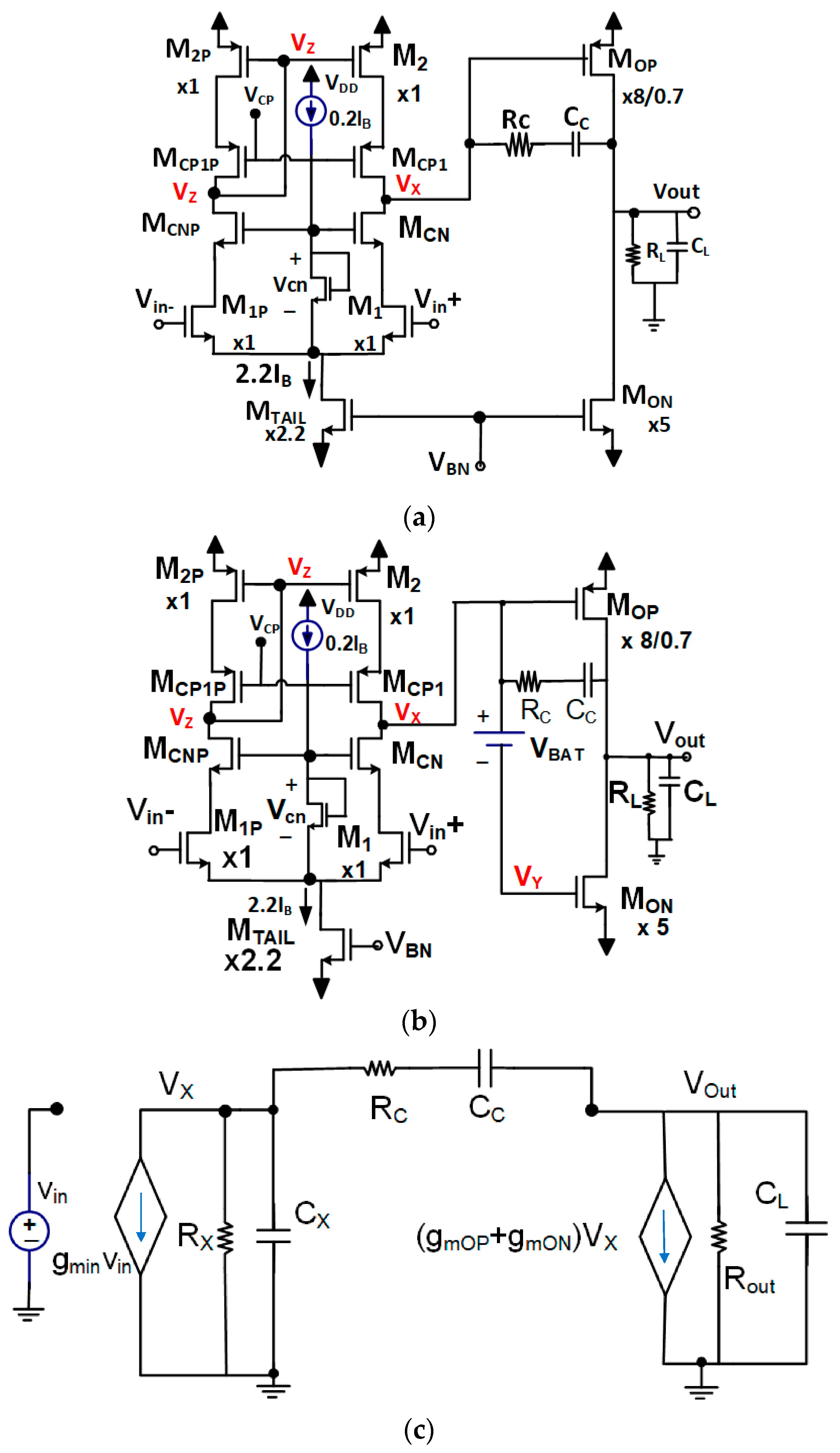
The Miller op-amp is the essential building block of analog integrated circuits [1,2]. In the conventional class-A Miller op-amp with an NMOS input stage [2,3] shown in Figure 1a, the NMOS output transistor limits the peak negative output current to a value IoutQ corresponding to the output branch’s quiescent current. This imposes a severe limitation in the op-amp’s negative slew rate (SR−). This can be expressed as SR− = (IoutQ − IRL)/(CC + CL), where CC and CL are compensation and load capacitors and IRL is the current of the resistive load. Many approaches have been proposed to implement Miller op-amps with static class-AB [4,5] output stages. This type of amplifier can drive a wide range of capacitive and resistive loads down to very low frequencies or DC. They are required to have approximately symmetrical slew rates and to be able to generate symmetrical peak load positive and negative output currents IOutpk+ and IOutpk− much larger than the total op-amp quiescent current ItotQ. A common figure of merit to characterize the op-amp current efficiency CE = IOutpk/ItotQ is defined as the ratio of the minimum of the positive and negative peak output currents IOutpk = MIN{IOutpk+, IOutpk−} to ItotQ. The conventional class-A op-amp (Conv-A) is characterized typically by CE < 0.5. Many approaches to implementing class-AB op-amps are based on the floating battery [6] scheme shown in Figure 1b. The floating battery that exists between the gates of the PMOS and NMOS output transistors causes the voltage VY at the gate of the output NMOS transistor to follow the variations at node VX, which is the high impedance output node of the differential input stage. The voltage VX drives the output PMOS transistor MOP. The small signal model of the class-AB op-amps based on the floating battery [6] scheme is shown in Figure 1c. In this, the ideal floating battery has been replaced by an AC short circuit. The output resistance ROut is given by ROut = RoOP||roON||RL. As the conventional Miller compensation is used in the op-amp, the transfer function of the circuit of Figure 1c can be written as Equation (1).
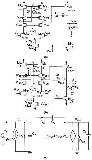
Figure 1.
(a) Conventional class-A Miller op-amp, (b) Miller op-amp with class-AB output stage based on floating battery, and (c) small-signal model of the class-AB op-amp based on the floating battery scheme.
Here, ωz, ωpOut, and ωpDOMX are given by the following expressions Equations (2)–(4).
where CX is given by CX = (1 + |AOut|) CC, RX = gmro2/2, and |AOut| is the gain of the output stage.
The operation of Class-AB op-amps based on the floating battery principle is discussed below:
- (a)
- Upon application of a positive step at Vin, the output of the op-amp provides a positive output current to the load. When the output slews in the positive direction, the voltage at node Vx is subject to a large negative variation, which is followed by the voltage at node VY until it reaches the bottom rail. This increases the current in MOP and decreases the current in MON, bringing it to zero for large negative variations in VY that lead to VGSON < VTN, where VTN is the threshold voltage of MON. Since VX can have large negative variations, the peak positive output current IOutpk+ provided by MOP can be much larger than its quiescent current IOutQ, and a large positive slew rate can be achieved. The situation is quite different for negative steps in Vin. In this case, VX has a relatively limited excursion in the positive direction, which is transferred (in practice with some attenuation) to VY. This causes the current in MOP to decrease (and eventually go to zero) and MON to increase. However, given that the variation in the positive direction of Vx and VY is much smaller than the variation in the negative direction, the op-amp’s peak negative output current IOutpk− generated by MON is in general much smaller than IOutpk+. This leads to a negative slew rate, which can be much smaller than the positive slew rate. In practice, the smaller of the two slew rates determines the nominal op-amp’s slew rate SR ≡ MIN{SR+, SR−}.
- (b)
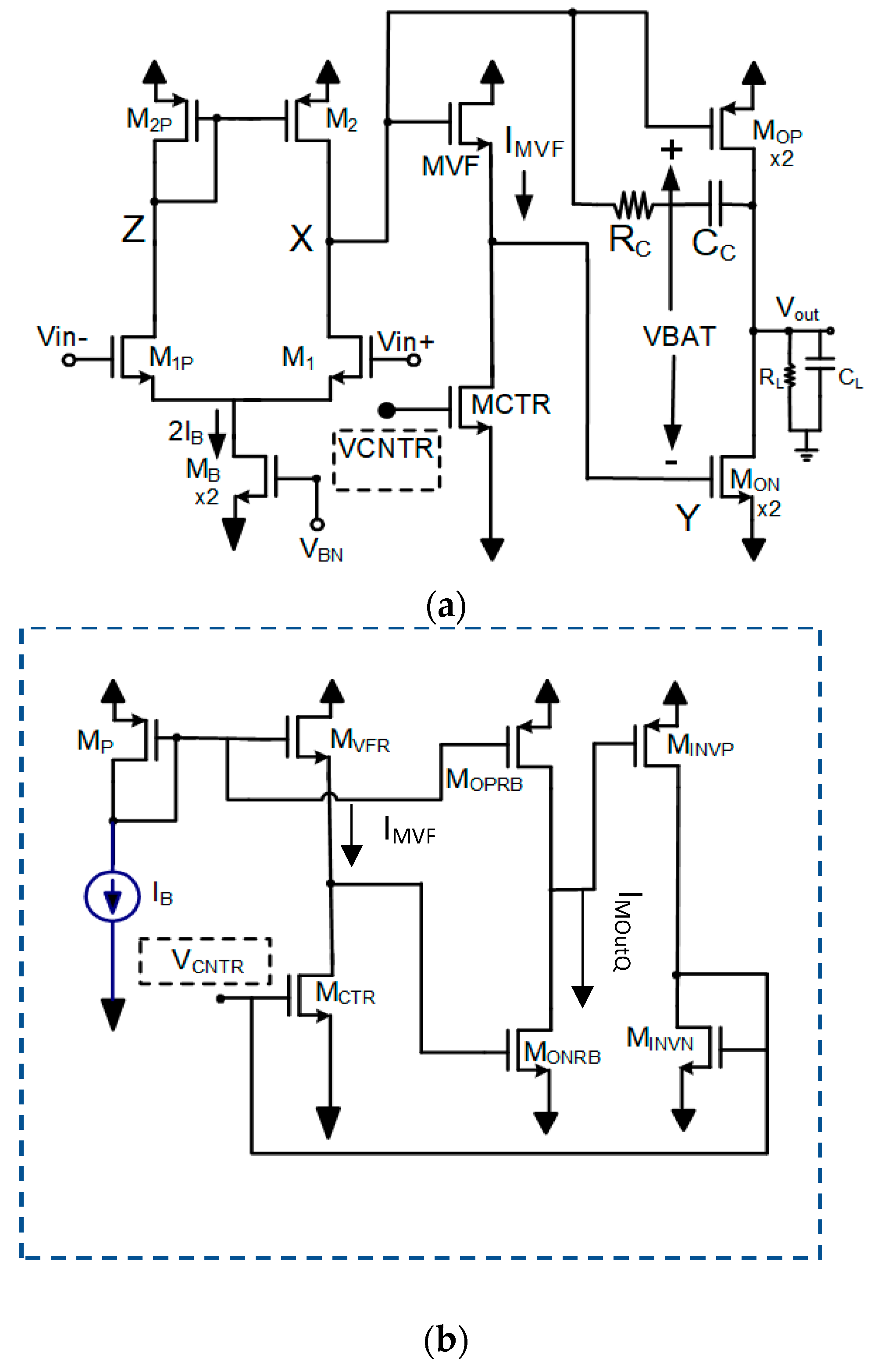
- The practical implementation of the floating battery scheme requires a control circuit to achieve the desired nominal output quiescent current IOutQ, which adjusts the value of the floating battery VBAT so that its value is well defined and remains constant, independent of temperature, process parameters, and supply voltage variations. It can be shown that, in saturation, IOutQ is approximately given by, where βN, βP, VTN, and VTP are the NMOS and PMOS output transistors’ gain factors and threshold voltages, respectively. A control circuit to adjust the value of VBAT is required since a fixed VBAT value would lead to large variations in IOutQ with changes in Vsupply, VTN, VTP, βN, or βP. An example of the class-AB output stage using a foating battery and a control circuit is shown in Figure 2. In this example, the floating battery is implemented using a voltage follower. The circuit implementation of both VBAT and the control circuit [7,8] can be relatively complex (as shown in Figure 2b and in the circuit of [8]) and increases the total op-amp’s quiescent current. This can significantly lower the current efficiency of the class-AB op-amp. In some cases, it can also increase the supply requirements beyond the nominal supply voltage of the implementation technology, which has been reduced to sub-volt values (Vsupply < 1 V) in modern CMOS technologies.
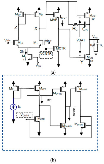 Figure 2. (a) Example of the class-AB output stage based on the floating battery principle using a VF with level shift and (b) a replica bias control circuit for the generation of VCNTR so that the quiescent output current has a nominal well-defined value independent of VDD, technology parameters, and temperature.
This paper introduces a simple scheme that overcomes the shortcomings discussed above, requiring minimal additional power dissipation and not increasing the supply requirements. This scheme is discussed in the next section. Traditionally, the performance of op-amps is compared using three well-known figures of merit: (a) the small-signal figure of merit FOMSS = fu·CL/PQ, where fu is the unity-gain frequency and PQ is the quiescent power of the op-amp; (b) the large-signal static current efficiency figure of merit FOMCEStat = IoutpkRL/PQ; and (c) the large-signal dynamic current efficiency figure of merit FOMCEDyn = SR·CL/PQ, which is related to the maximum dynamic output current in load capacitance CL. FOMCEStat is determined by the maximum DC output current in the load resistor RL (denoted IoutpkRL) relative to the total quiescent power PQ of the op-amp. In addition, as both FOMSS and FOMCEDyn determine the ultimate speed of an op-amp, a new global figure of merit FOMGlobal given by is also used here.
2. Circuit Description
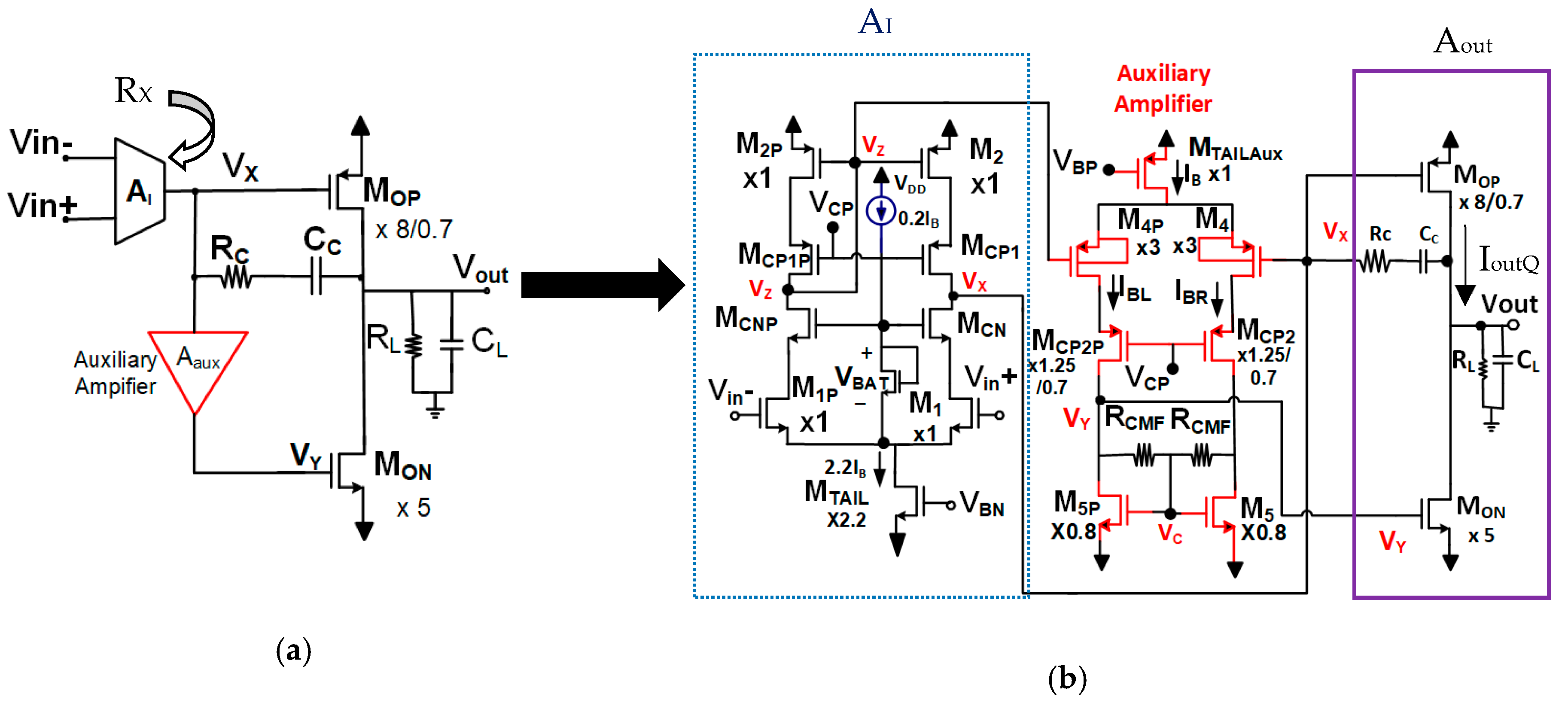
The scheme of the proposed op-amp is shown in Figure 3a. A telescopic input stage is used in the first stage to achieve high gain even in the presence of a low-valued load resistor RL (high loading conditions) that can degrade the second stage gain significantly. The proposed op-amp uses an auxiliary non-inverting amplifier with gain Aaux to generate a voltage variation VY, which is an amplified version of the variations in VX, that is, VY = AauxVX. This auxiliary amplifier consumes less than 10% of the op-amp’s total bias current and does not increase supply requirements. The transistor-level implementation of the auxiliary amplifier is shown in Figure 3b. It uses a differential stage with resistive common-mode feedback (RCMFB) that has approximately a gain Aaux = (gm4RCMF)/2, as shown in the analysis below. The auxiliary amplifier increases the op-amp’s output negative current; the open-loop DC gain shifts the output poles to the higher frequency, allowing for a higher unity gain frequency. The quiescent voltage of VY has a value VYQ = VGSQM5P independent of RCMF (and of AAux). This allows to accurately control the quiescent current IOutQ in the op-amp’s output branch independent of the gain Aaux, supply voltage, technology parameters variations, and temperature changes. Given that the variations generated at VY are amplified with respect to those at Vx, MON can provide large negative output currents even though the amplitude of positive variations in VX is smaller than that for negative variations. This overcomes one of the limitations of the conventional battery approach shown in Figure 1b.
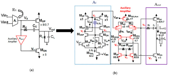
Figure 3.
(a) Scheme of the proposed class-AB Miller op-amp and (b) transistor level implementation.
In order to prevent degradation of the phase margin of the op-amp, the value of RCMF (and Aaux) is chosen in such a way that the pole at node Y is higher than the unity gain frequency fu of the op-amp by at least a factor of 3. Thus, the selection of the optimal value of RCMF is the crucial factor for the design of the proposed auxiliary amplifier. Larger values of RCMF lead to enhanced negative output currents and gains, resulting in lower values for the pole at node Y and lower phase margin.
In the presence of positive signals in VX larger than VSDsat4, all of the tail current of MTAILAUX flows through M4P and RCMF. This causes a large positive voltage change at node VY that generates large negative op-amp output currents. In order to achieve similar peak positive and negative output currents with the selected value of RCMF, the output transistors MON and MOP are scaled by factor 5/1 and factor 8/0.7 with respect to the unit PMOS and NMOS transistors of size 10/0.27 used in the input stage. In addition, conventional Miller compensation is used to achieve stability.
2.1. Operation
The working principle of the proposed op-amp can be explained by considering its voltage follower operation. In the presence of the positive input signal Vin, the voltage at node VX decreases and the voltage at node VY also decreases by a factor Aaux. As a result, MOP provides a large positive current, and the drain current of MON decreases and eventually reaches zero. On the other hand, for negative input signals, the voltage at node VY corresponds to the amplified version of the positive signals of node VX, which is VY = AauxVX. As a result, MON can also provide large negative output currents.
2.2. Frequency Response
Conventional Miller compensation is used in the proposed op-amp. The proposed op-amp has one dominant pole ωpDOMX at node VX and two high-frequency poles ωpY and ωpOut. The zero ωz approximately nullifies the effect of ωpOut.
Thus, the transfer function of the proposed op-amp is given by Equation (5).
The gain of the first stage AI is given by Equation (6).
Here, for simplicity, gm is the transconductance gain of all unit size NMOS and PMOS transistors, ro is their output resistance, and RX is resistance at node VX. The auxiliary amplifier’s gain is given by Aaux = (gm4RY)/2, where . As RCMF << ro4P, roCP2P, ro5P, RY ≈ RCMF and Aaux ≈ (gm4RCMF)/2.
The gain of the output stage is given by Equation (7).
where ROut is .
Thus, the open-loop DC gain AOLDC of the proposed op-amp is expressed by Equation (8).
where gmouteff = gmOP + AauxgmON and ROut = rOP||rON||RL.
The dominant pole is at node VX and is given by Equation (9).
where CX is given by CX = (1 + |Aout|) CC.
Thus, the gain-bandwidth product (GBW) of the proposed op-amp is given by Equation (10).
Besides the dominant pole, the proposed op-amp has two high-frequency poles: one at VY and another at VOut. The output high-frequency pole fpOut is given in Equation (11).
The pole at node VY is expressed by Equation (12).
where CY is given by and . The selection of RCMF plays an important role in determining a compromise between the gain of the auxiliary amplifier and the phase margin of the op-amp. To achieve a sufficient phase margin, fPY should be higher than the unity gain frequency of the op-amp. Thus, RCMF has to be selected in such a way that the pole of the node Y, i.e., fPY, is located at least a factor three higher than the op-amp’s unity gain frequency, and in that case, RCMF << ro5P,ro4PgmCP2ProCP2P and RY can be approximated as RY ≈ RCMF. In this case, fPY has a minor effect on the op-amp’s frequency response up to the unity gain frequncy fu, and Equation (12) can be simplified as below.
The zero is given by Equation (14).
The simplified transfer function of the proposed op-amp neglecting the pole at node Y can be approximated by Equation (15).
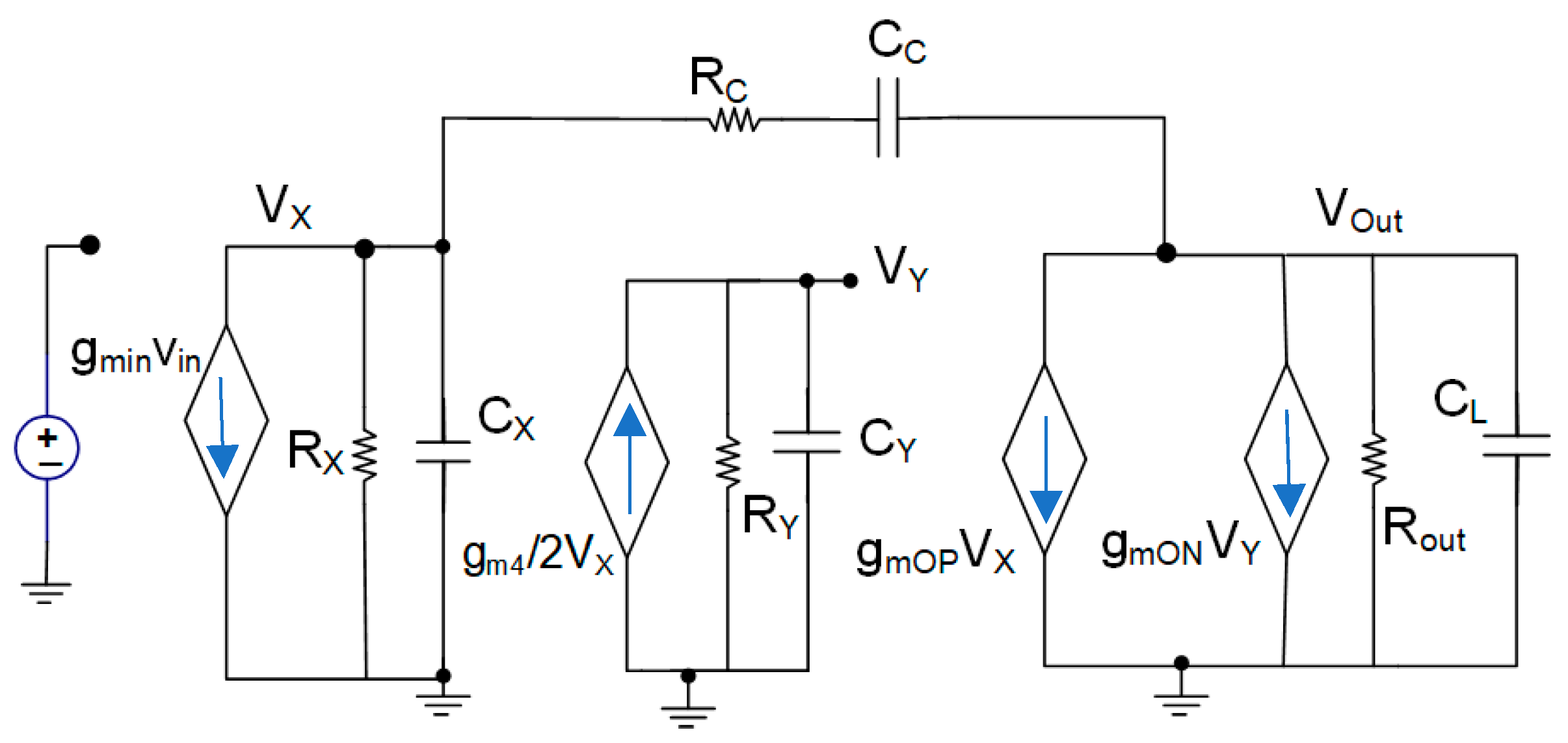
The small-signal model of the proposed op-amp is given in Figure 4.
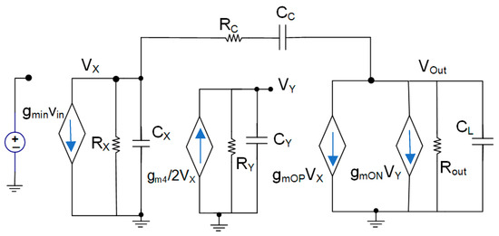
Figure 4.
Small-signal model of the proposed op-amp.
3. Results
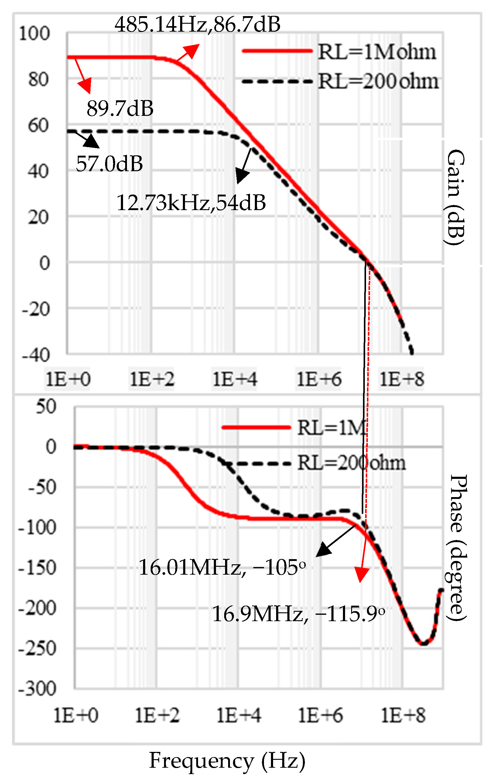
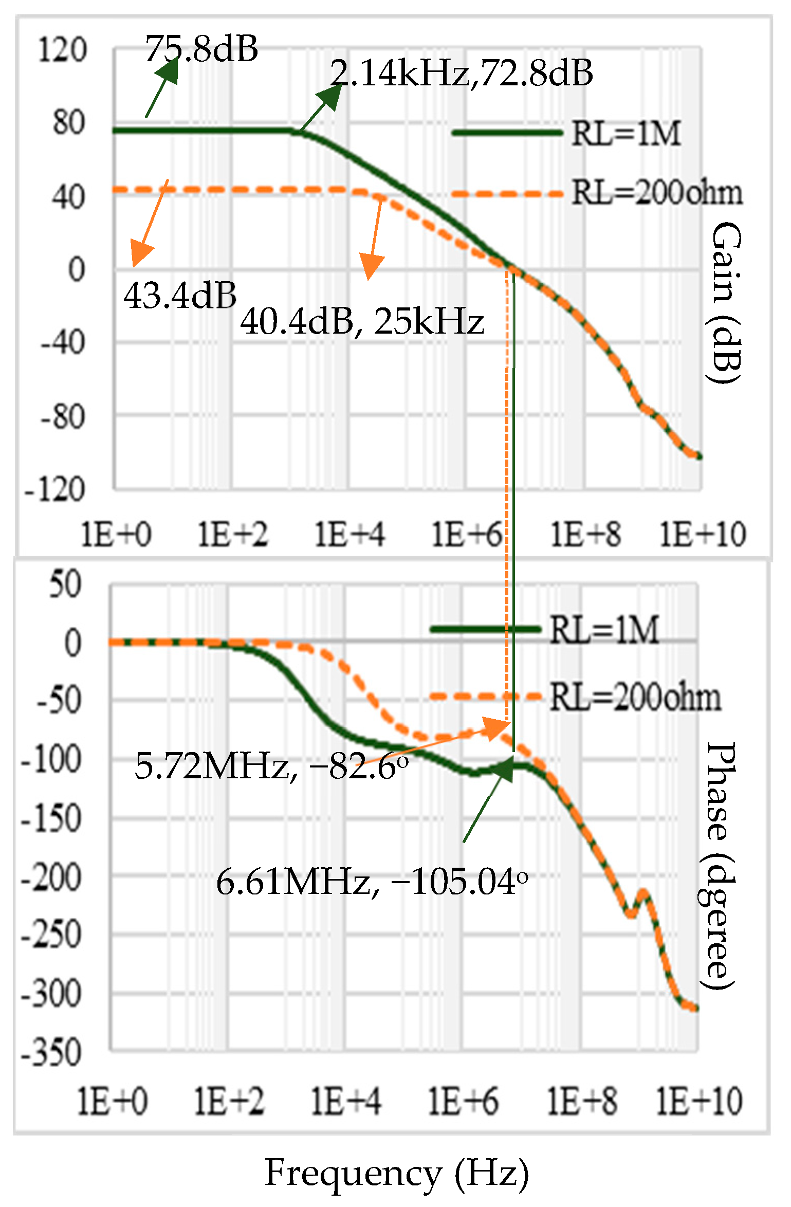
The proposed and conventional class-A op-amps are designed in 130 nm CMOS technology. The unit size transistors used in both op-amps are (W/L)N = (W/L)P = 10/0.27 (µm/µm). The compensation capacitor has a value CC = 4 pF for both op-amps. The compensation resistor RC has a value 8 kΩ for the proposed op-amp and 19 kΩ for the Conv-A op-amp. For a fair comparison, the output transistors of the Conv-A op-amp MOP are scaled by the same factor 8/0.7 and MON is by the same factor 5/1 as the proposed op-amp compared to the unit size transistors used in the circuit. They are simulated using the same bias current IB = 15 µA, and dual supply voltages VDD = +0.6 V and VSS = −0.6 V. Figure 5 shows the open-loop frequency response of the proposed op-amp. The proposed op-amp has open-loop gains AOLDC = 89.7 dB with RL = 1 MΩ and 57 dB with RL = 200 Ω, and CL = 300 pF in both cases. On the other hand, the conventional class-A(Conv-A) op-amp can provide a maximum AOLDC of 75.8 dB for RL = 1 MΩ and only 43.4 dB with RL = 200 Ω. Figure 6 shows the corresponding frequency response of the Conv-A op-amp with CL = 300 pF.
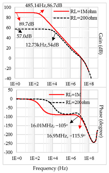
Figure 5.
Frequency response of the proposed op-amp in open-loop configuration for RL = 1 MΩ and RL = 200 Ω.
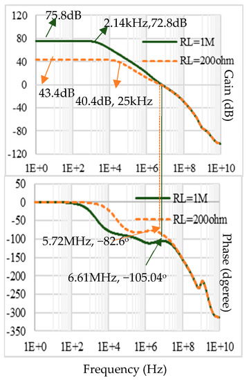
Figure 6.
Open-loop frequency response of the Conv-A op-amp for RL = 1 MΩ and RL = 200 Ω.
The unity gain frequency fu of the proposed op-amp for RL = 1 MΩ is 16.9 MHz and for RL = 200 Ω is 16.01 MHz. The small-signal figures of merit FOMSS of the proposed op-amp are 28.8 and 27.2 for RL = 1 MΩ and 200 Ω. The Conv-A op-amp’s FOMSS for similar loading conditions are 12.4 and 10.8. Thus, the proposed op-amp can drive a low-value resistive load (high-loading condition) by maintaining a relatively high open-loop gain. It can be seen that, as expected, the introduction of the auxiliary amplifier in the proposed op-amp leads to lower gain degradation (and consequently, lower gain errors) for lower-valued load resistors.
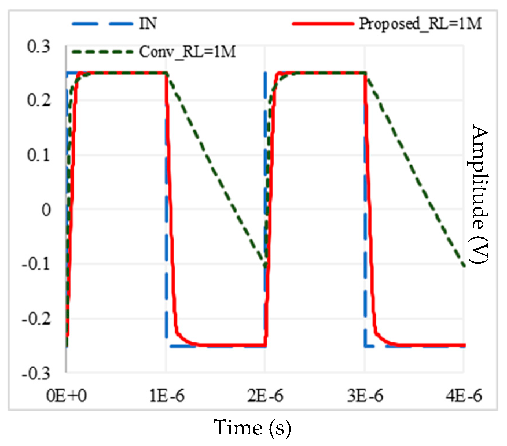
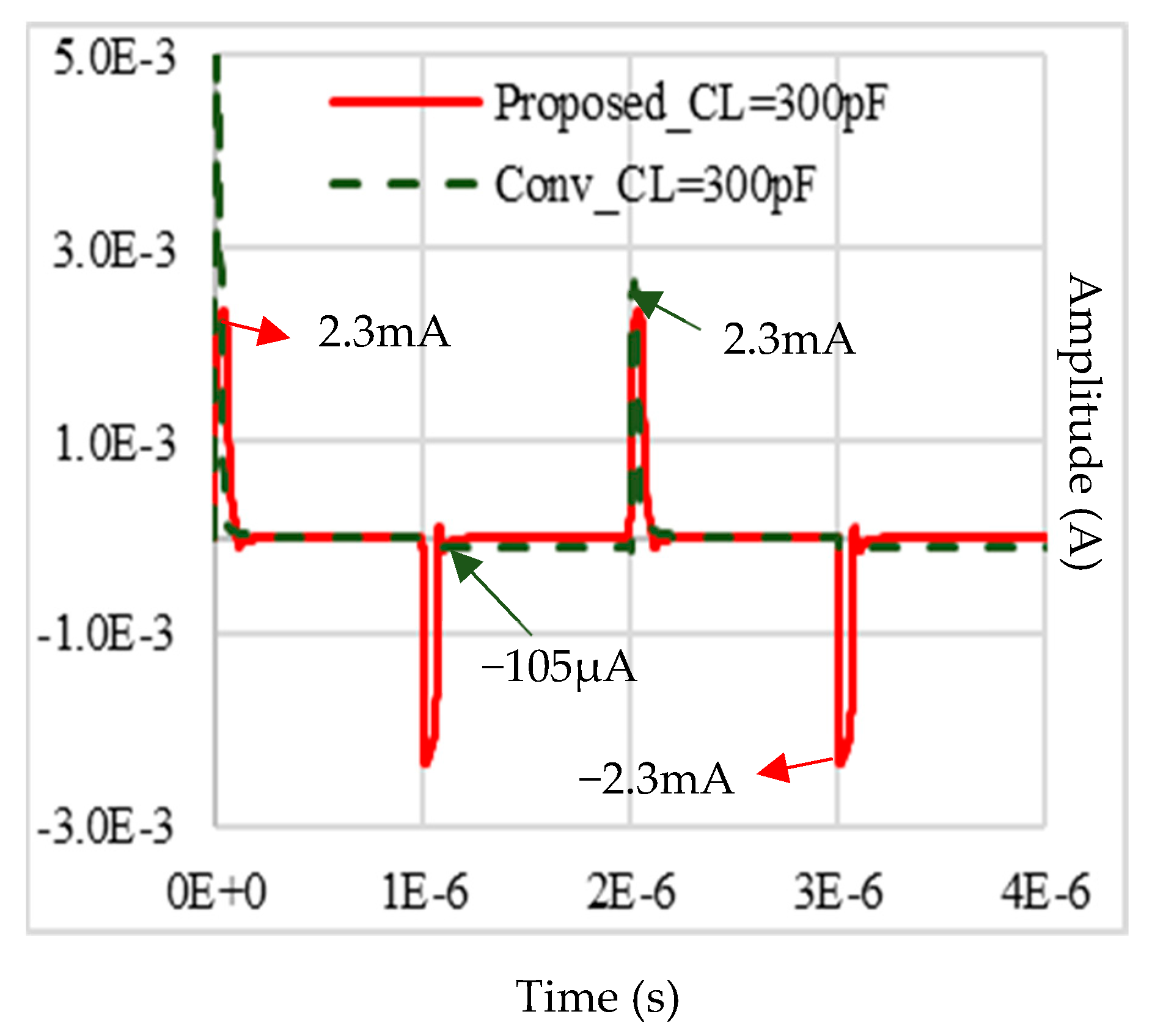
Figure 7 shows the transient response of the proposed and Conv-A op-amp with RL = 1 MΩ and CL = 300 pF for a 500 kHz input pulse with 500 mVpp amplitude. It can be observed that the Conv-A op-amp cannot follow the input signal. From Figure 8, it can be asserted that this is because of the limitation of the peak negative output current, which corresponds to the quiescent current of the output branch in the Conv-A op-amp. From the pulse responses and load currents of the proposed and Conv-A op-amp for RL = 1 MΩ, it can be asserted that the proposed op-amp increases the negative slew rate by a factor of 20 compared with the Conv-A op-amp. The SR enhances by a large factor close to 20 from 0.36 V/µs for the Conv-A to 7.4 V/µs for the proposed op-amp. Therefore, the CE of the proposed and Conv-A op-amps are 15.6 and 0.8, respectively.
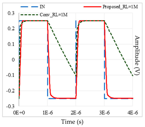
Figure 7.
Transient response of the Conv-A and proposed op-amps for 500 kHz and 500 mVpp amplitude input pulses with RL = 1 MΩ and CL = 300 pF.
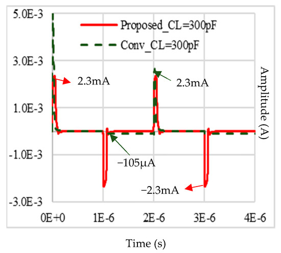
Figure 8.
Current in the load capacitance CL = 300 pF in the Conv-A and proposed op-amps for 500 kHz and 500 mVpp amplitude pulse inputs.
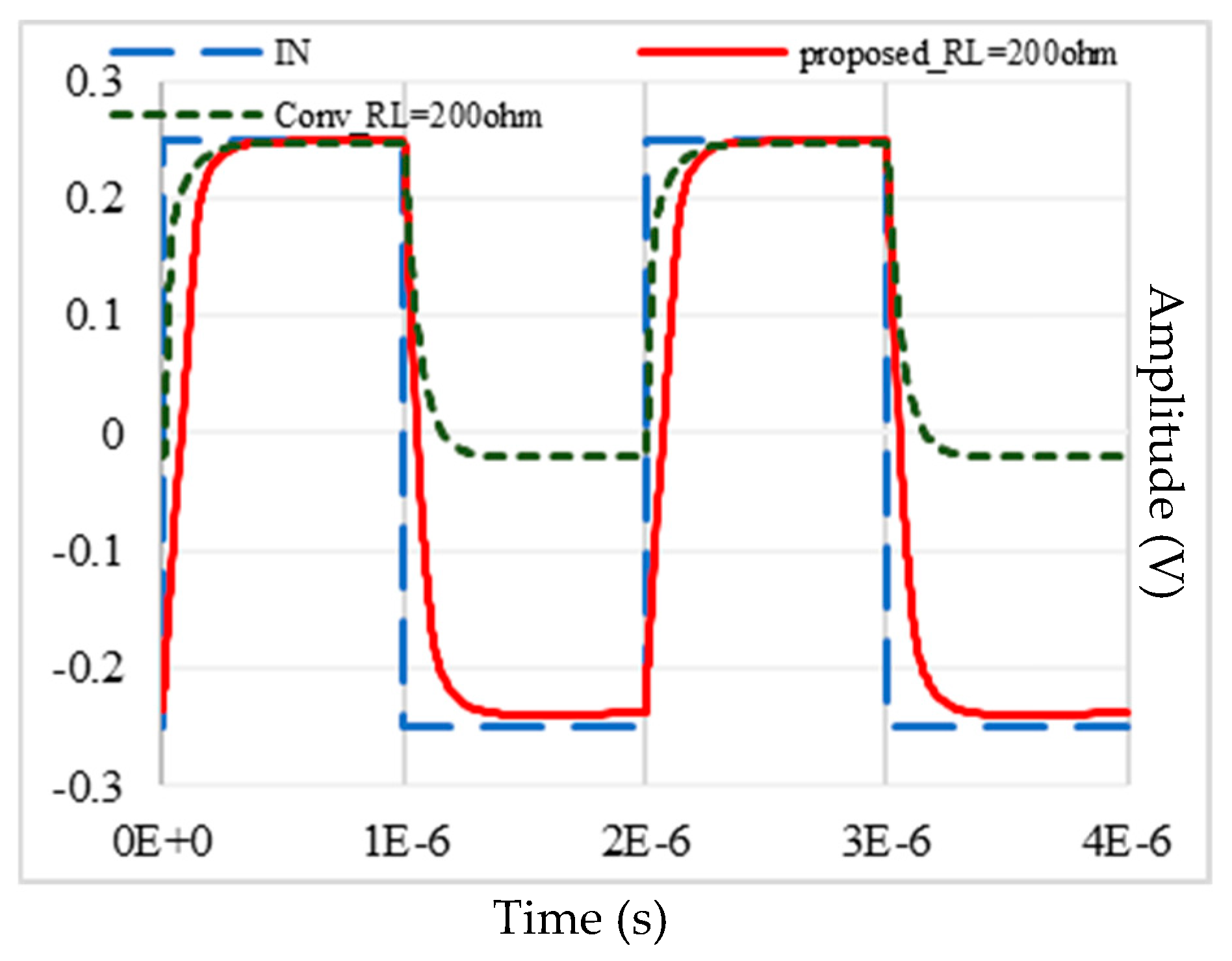
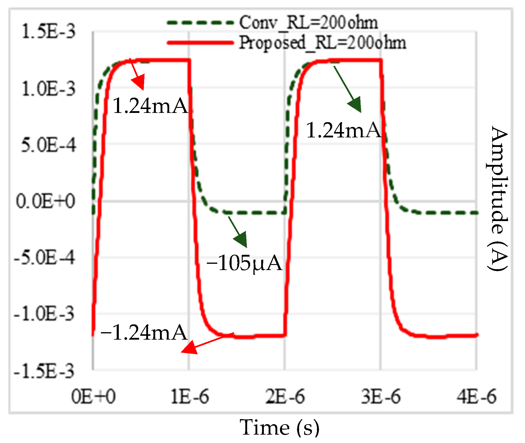
From Figure 9, it can be asserted that the proposed op-amp can drive both large capacitive and low-valued resistive loads. Figure 10 shows the output current in the 200 Ω load resistor for the Conv-A and proposed op-amps for 500 mVpp and 500 kHz input pulse. It can be seen that the proposed op-amp can provide 1.24 mA positive and negative peak output currents to a 200 Ω resistive load for a 500 mVpp and 500 kHz input pulse. In contrast, the Conv-A op-amp with the same input signal can provide only a 105 A negative output current, which is limited by the quiescent current of the output branch.
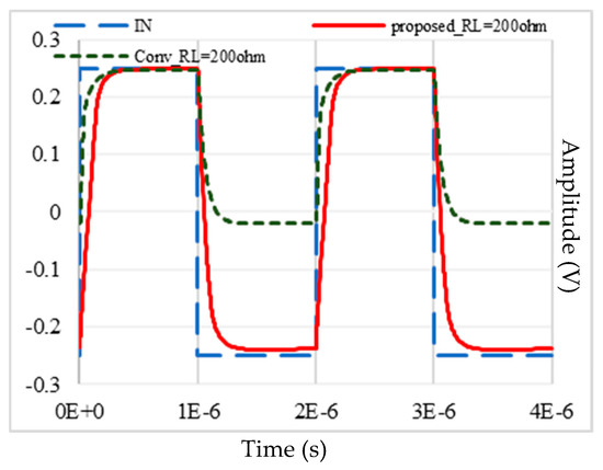
Figure 9.
Transient response of the Conv-A and proposed op-amps for 500 kHz and 500 mVpp pulse inputs with RL = 200 Ω and CL = 300 pF.
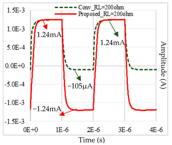
Figure 10.
Current in RL = 200 Ω in the Conv-A and Proposed op-amps 500 kHz and 500 mVpp amplitude pulse inputs.
Figure 11 and Figure 12 show the closed-loop frequency response of the proposed and Conv-A op-amps in the voltage follower configuration (VF). The proposed op-amp has 3 dB.
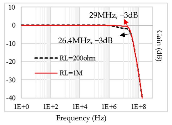
Figure 11.
Frequency response of the proposed op-amp in a close-loop VF configuration for RL = 1 MΩ and RL = 200 Ω.
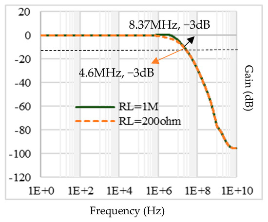
Figure 12.
Closed-loop frequency response of the conventional class-A op-amp for RL = 1 MΩ and RL = 200 Ω in the VF mode.
The bandwidth (BW) is 29 MHz for RL = 1 MΩ and 26.4 MHz for RL = 200 Ω. In comparison, the Conv-A op-amp has 8.37 MHz and 4.6 MHz 3 dB bandwidths for similar loading conditions. It can be seen that the proposed op-amp has a higher bandwidth than the Conv-A op-amp.
A corner analysis of the proposed op-amp was performed to verify its robustness against temperature, process variations, and mismatches in the values of the design components. Table 1 shows the corner analysis of the op-amp employing typical 2% mismatches in the differential pair and the resistors used in the auxiliary amplifier. It can be asserted that, from the corner analysis, the proposed op-amp is robust against the temperature and process variations.

Table 1.
Corner analysis of the op-amp at different temperatures.
Figures of merit FOMCEDyn and FOMCEStat of the proposed op-amp are 12.6 and 7. FOMCEDyn and FOMCEStat of the Conv-A op-amp are 0.8 and 0.66. Thus, the proposed op-amp achieved 16 times higher FOMCEDyn and 10.6 times higher FOMCEStat than the Conv-A op-amp.
Comprehensive comparisons of the proposed op-amp’s performance with state-of-the-art op-amps and Conv-A op-amp are shown in Table 2. The proposed op-amp has the highest small-signal, dynamic, static current efficiency, and global figures of merits. It can be asserted that, from the comparison table, the proposed architecture can drive both resistive and capacitive load efficiently. The presence of the auxiliary amplifier in the prosed architecture makes this possible.

Table 2.
Summary of the results and performance comparison.
4. Conclusions
A simple class-AB Miller op-amp that can drive both resistive and capacitive loads is presented here. A compact auxiliary amplifier is used to provide the static class-AB operation and helps to achieve higher gain, bandwidth, and a well-defined output quiescent current. The proposed op-amp can provide a 13.9 dB higher open-loop gain, a factor 20 higher slew-rate, and a factor 3.3 to 5.7 higher bandwidth (in VF configuration) than the conventional op-amp at the expense of only 10% additional quiescent current compared to the Conv-A op-amp.
Author Contributions
Investigation, writing, review, and editing were completed by A.P., M.R.-P., J.R.-A., R.B.-P., H.V.-L., J.H.-C. and A.D.-S. All authors have read and agreed to the published version of the manuscript.
Funding
This work was supported in part by the Mexican Consejo Nacional de Ciencia y Tecnologia (CONACYT) under grant A1-S-43214.
Data Availability Statement
Data is contained within the article.
Acknowledgments
The authors thank MOSIS for providing the simulation model.
Conflicts of Interest
There are no conflicts of interest.
References
- Cruz, S.C.D.; Reyes, M.G.T.D.; Gaffud, T.C.; Abaya, T.V.F.; Gusad, M.T.A.; Rosales, M.D. Design and implementation of operational amplifiers with programmable characteristics in a 90 nm CMOS process. In Proceedings of the 2009 European Conference on Circuit Theory and Design, Antalya, Turkey, 23–27 August 2009; pp. 209–212. [Google Scholar]
- Razavi, B. Design of Analog CMOS Integrated Circuits; McGraw-Hill: New York, NY, USA, 2001. [Google Scholar]
- William, S.M.C. Analog Design Essentials; Springer: New York, NY, USA; Berlin, Germany, 2006. [Google Scholar]
- Monticelli, D.M. A quad CMOS single-supply op amp with rail-to-rail output swing. IEEE J. Solid State Circuits 1986, 21, 1026–1034. [Google Scholar] [CrossRef] [Green Version]
- De Langen, K.-J.; Huijsing, J. Compact low-voltage power-efficient operational amplifier cells for VLSI. IEEE J. Solid State Circuits 1998, 33, 1482–1496. [Google Scholar] [CrossRef] [Green Version]
- Gregorian, R.; Temes, G.C. Analog MOS Integrated Circuits for Signal Processing; Wiley Series on Filters: Design Manufacturing and Applications; Wiley-Interscience: New York, NY, USA, 1986. [Google Scholar]
- Torralba, A.; Carvajal, R.G.; Ramirez-Angulo, J.; Tombs, J.; Galán, T. Class AB output stages for low voltage CMOS opamps with accurate quiescent current control by means of dynamic biasing. In Proceedings of the ICECS 2001 8th IEEE International Conference on Electronics, Circuits and Systems (Cat. No.01EX483), Malta City, Malta, 2–5 September 2001; Volume 2, pp. 967–970. [Google Scholar] [CrossRef]
- Padilla-Cantoya, I.; Molinar-Solis, J.E.; Medina-Vazquez, A.S.; Gurrola-Navarro, M.A.; Rizo-Dominguez, L.; Gutierrez-Frias, E.F. Class AB Op-Amp with Accurate Static Current Control for Low and High Supply Voltages. IEEE Trans. Circuits Syst. II Express Briefs 2021, 1. [Google Scholar] [CrossRef]
- Sutula, S.; Dei, M.; Terés, L.; Serra-Graells, F. Variable-Mirror Amplifier: A New Family of Process-Independent Class-AB Single-Stage OTAs for Low-Power SC Circuits. IEEE Trans. Circuits Syst. I Regul. Pap. 2016, 63, 1101–1110. [Google Scholar] [CrossRef] [Green Version]
- Cabrera-Bernal, E.; Pennisi, S.; Grasso, A.D.; Torralba, A.; Carvajal, R.G. 0.7-V Three-Stage Class-AB CMOS Operational Transconductance Amplifier. IEEE Trans. Circuits Syst. I Regul. Pap. 2016, 63, 1807–1815. [Google Scholar] [CrossRef]
- Anisheh, S.M.; Abbasizadeh, H.; Shamsi, H.; Dadkhah, C.; Lee, K.-Y. 98-dB Gain Class-AB OTA with 100 pF Load Capacitor in 180-nm Digital CMOS Process. IEEE Access 2019, 7, 17772–17779. [Google Scholar] [CrossRef]
- Grasso, A.D.; Pennisi, S.; Scotti, G.; Trifiletti, A. 0.9-V Class-AB Miller OTA in 0.35μm CMOS with Threshold-Lowered Non-Tailed Differential Pair. IEEE Trans. Circuits Syst. I Regul. Pap. 2017, 64, 1740–1747. [Google Scholar] [CrossRef]
- Kuo, P.-Y.; Tsai, S.-D. An Enhanced Scheme of Multi-Stage Amplifier with High-Speed High-Gain Blocks and Recycling Frequency Cascode Circuitry to Improve Gain-Bandwidth and Slew Rate. IEEE Access 2019, 7, 130820–130829. [Google Scholar] [CrossRef]
- Renteria-Pinon, M.; Ramirez-Angulo, J.; Diaz-Sanchez, A. Simple Scheme for the Implementation of Low Voltage Fully Differential Amplifiers without Output Common-Mode Feedback Network. J. Low Power Electron. Appl. 2020, 10, 34. [Google Scholar] [CrossRef]
Publisher’s Note: MDPI stays neutral with regard to jurisdictional claims in published maps and institutional affiliations. |
© 2021 by the authors. Licensee MDPI, Basel, Switzerland. This article is an open access article distributed under the terms and conditions of the Creative Commons Attribution (CC BY) license (https://creativecommons.org/licenses/by/4.0/).

