Article

An Innovative Successive Approximation Register Analog-to-Digital Converter for a Nine-Axis Sensing System

Department of Electronic Engineering, National Chiao Tung University, Hsinchu 300, Taiwan
*
Author to whom correspondence should be addressed.
J. Low Power Electron. Appl. 2021, 11(1), 3; https://doi.org/10.3390/jlpea11010003
Submission received: 23 November 2020 / Revised: 18 December 2020 / Accepted: 6 January 2021 / Published: 9 January 2021

Abstract

:
With nine-axis sensing systems in 5G smartphones, mobile power consumption has become increasingly important, and ultra-low-power (ULP) sensor circuits can decrease power consumption to tens of microwatts. This paper presents an innovative successive approximation register analog-to-digital converter, which comprises fine (three most significant bits (MSBs) plus course conversion (11 least significant bits (LSBs)) capacitive digital-to-analog converters (CDACs), ULP, four-mode reconfigurable resolution (9, 10, 11, or 12 bits), an internally generated clock, meta-detection, the switching base midpoint voltage (Vm) (SW-B-M), bit control logic, multi-phase control logic, fine (three MSBs) plus course conversion (11 LSBs) switch control logic, phase control logic, and an input signal plus negative voltage (VI + NEG) voltage generator. Then, the mechanism of the discrete Fourier transform (DFT)-based calibration is applied. The scalable voltage technique was used, and the analog/digital voltage was Vanalog (1.5 V) and Vdigital (0.9 V) to meet the specifications of the nine-axis ULP sensing system. The CDACs can reconfigure four-mode resolutions, 9–12 bits, for use in nine-axis sensor applications. The corresponding dynamic signal-to-noise and distortion ratio performance was 50.78, 58.53, 62.42, and 66.51 dB. In the 12-bit mode, the power consumption of the ADC was approximately 2.7 μW, and the corresponding figure of merit (FoM) was approximately 30.5 fJ for each conversion step.

1. Introduction

A recent trend is the application of nine-axis sensing systems that merge analog radio frequency microelectromechanical systems (RF MEMSs) with 5G mobile systems. These nine-axis ultra-low-power (ULP) sensing systems have been important for increasing mobile standby time and maintaining high-efficiency operations. In the power consumption of the capacitance-to-digital (C2D) circuit, the contribution of the analog-to-digital converter is the largest. To meet the specifications of the nine-axis ultra-low-power (ULP) sensing systems, the power consumption of the analog-to-digital converter which is less than 10 uW is needed. For example, the three-axis accelerometer is a capacitive sensing system, and the capacitance variation for per G, which is acceleration, is often smaller than 1 fF/G. Capacitance-to-voltage (C2V) circuits, correlated double sampling (CDS), and chopper stabilization (CHS) are used to decrease low-frequency noise. The capacitance-to-digital (C2D) circuit also needs a variable gain amplifier (VGA) to amplify sensing signals. The C2D circuit uses time-sharing, a time-division multiplexing method to increase standby time. The output voltage of a three-axis accelerometer is pulled to the successive approximation register analog-to-digital converter (SAR-ADC) with a fine (three most significant bits (MSBs)) plus course conversion (11 least significant bits (LSBs)) capacitive digital-to-analog converter (CDA). This SAR-ADC with a fine plus course conversion CDA (SAR-ADC-WFC-CDA) has an internally generated clock. Discrete Fourier transform (DFT)-based calibration is applied to reduce the performance decline. The SAR-ADC-WFC-CDA chooses a ULP four-mode reconfigurable resolution (RR). The internally generated clock is generated by an internal circuit. A thermometer code is used to switch the segment capacitors and to decrease the transient noise for the fine conversion capacitive digital-to-analog converter (CDAC).
In this study, the non-binary weighted method was used to avoid the incomplete CDAC settling time problems caused by course conversion CDAC errors. Error correction, which increases the digital code correction capability, and meta-detection, which avoids the occurrence of spark codes, were applied. The switching base midpoint voltage (Vm) (SW-B-M) was used to decrease the average switching energy. A dynamic latch was used to increase the data input (Din) speed, bit control logic, multi-phase control logic, fine (three MSBs) plus course (11 LSBs) conversion switch control logic, phase control logic, and an input signal plus the negative voltage (VI + NEG) voltage generator. A switch with NEG (SW-W-NEG) was used to increase the linearity and to reconfigure the 9-, 10-, 11-, and 12-bit resolutions.
Moreover, fully-synthesizable successive approximation register (SAR) analog-to-digital converters (ADCs) were presented and the dyadic digital pulse modulation (DDPM) digital-to-analog (DAC) was used and FOM is higher than the traditional SAR-ADC [1]. An energy-efficient low power 10-b 8-MS/s asynchronous successive approximation register (SAR) analog-to-digital (ADC) converter was presented and the power consumption is 108 uW [2]. The method of the estimated lower bound to the power consumption of successive approximation analog-to-digital converters is presented [3] and FOM is 94.5 fJ/conversion. A recursive discrete Fourier transform (RDFT) foreground digital calibration method is used to lower the harmonic distortion [4] and power consumption is 41.5 μW. A reconfigurable successive approximation register (SAR) analog-to-digital converter (ADC), where the resolution can be scaled from 9 to 12 bits, is used to lower power consumption [5] and power consumption is 9.7 μW for the 12-bit mode.

1.1. Analysis of the Switching Base Vm (SW-B-M) Algorithm and Architecture

Figure 1 illustrates the SW-B-M architecture and binary-weighted CDAC. The following is the SW-B-M procedure: In the sample phase, the bootstrap switch pulls to input differential signals (VIP and VIN), and the CDAC on the upper-side and the top plate is the VIP signal. The midpoint voltage (Vm) pulls to the CDAC on the bottom plate. In Phase 1, the bootstrap switch is floated. The two-stage comparator can compare the input of the differential voltages (node_p and node_n) to decide directly and does not change any capacitors. The maximum capacitor (P1C) on the upper-side and the bottom plate connect from the Vm to the high-level voltage (VH) when the node_p voltage is greater than the node_n voltage. The maximum capacitor (N1C) on the lower-side and the bottom plate connect from the Vm to the low-level voltage (VL). The SW-B-M repeats this operation until the LSB makes a decision [6].
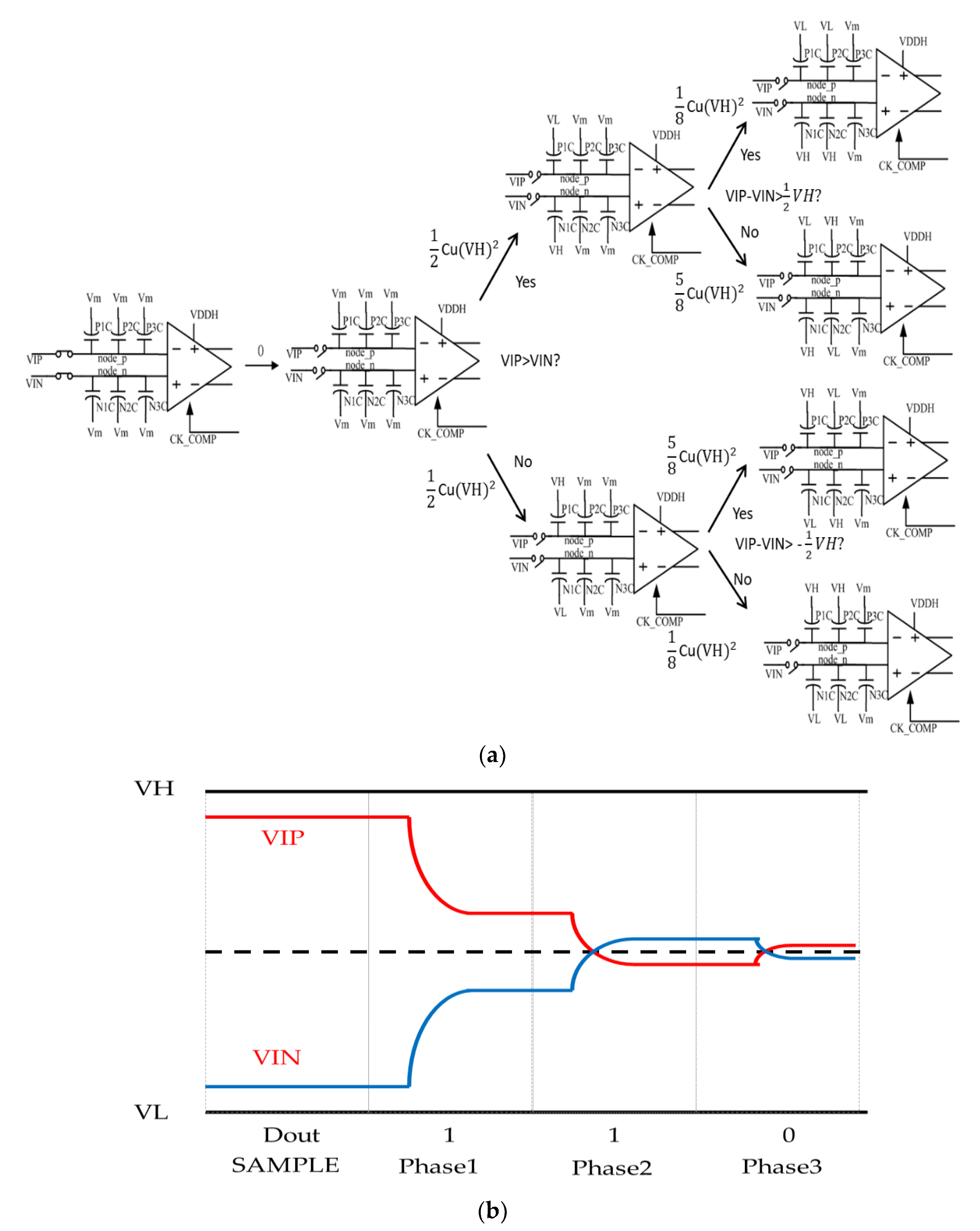
Figure 2a presents the SW-B-M switching procedure. A binary search CDAC is used and generates both the voltage of node_p and node_n through charge redistribution [7]. It shows the 3-bit binary-weighted CDAC with the SW-B-M [8]. In the sample phase, both input differential signals (VIP and VIN) are sampled with the CDAC top plates, and the bottom plates of the two CDACs are connected to the Vm. In Phase 1, the VIP and VIN are floated. In Phase 2, the MSB CDAC on the upper-side and the bottom plate is connected from the Vm to the VH, and the MSB CDAC on the lower-side and the bottom plate is pulled down from the Vm to the VL. The rest of the capacitors on the bottom plate are then connected to the Vm. Figure 2b presents the waveform of the SW-B-M switching procedure. Equations (1) and (5) use the law of charge conservation from sample phase to phase 1, while Equations (2) and (6) can be used to calculate the upper- and the lower-sides of the top plate voltage (node_p and node_n). Equations (3) and (7) can be used to determine the voltage node_p and node_n from phase 1 to phase 2. The energy consumption from phase 1 to phase 2 for the upper- and lower-sides can be derived from Equations (4) and (8), and the total energy can be derived from Equation (9). The total energy can be derived from Equation (10) when Vm is equal to half of the VH. The average switching energy of the capacitor by the SW-B-M method is represented by Equation (11):
( V m + V I P ) 4 C u = ( V n o d e _ p V H ) 2 C u + ( V n o d e _ p V m ) 2 C u
V n o d e _ p = 1 2 V H   1 2 V m + V I P
V n o d e _ p p h a s e 1 p h a s e 2 = 1 2 V H 1 2 V m + V I P V H ( V m + V I P )
E n e r g y p p h a s e 1 p h a s e 2 = ( V H V m ) 2 C u V n o d e _ p p h a s e 1 p h a s e 2
( V m + V I N ) 4 C u = ( V n o d e _ n 0 ) 2 C u + ( V n o d e _ n V m ) 2 C u
V n o d e _ n = 1 2 V m + V I N 0
V n o d e _ n p h a s e 1 p h a s e 2 = 1 2 V m + V I N 0 ( V m + V I N )
E n e r g y n p h a s e 1 p h a s e 2 = ( V H V m ) 2 C u V n o d e _ n p h a s e 1 p h a s e 2
E n e r g y p p h a s e 1 p h a s e 2 + E n e r g y n p h a s e 1 p h a s e 2      = ( ( V H + V m ) 2 ) C u ) + ( ( V H + V m ) C u V m ) )          = ( C u V H 2 ) + ( C u V H V m )
S e t   V m = 1 2 V H ;   E n e r g y p p h a s e 1 p h a s e 2 + E n e r g y n p h a s d e 1 p h a s e 2 = 1 2 C u ( V H ) 2
E S W B M , a v g = i = 1 n 1 2 n 3 2 i · ( 2 i 1 ) · C u · ( V H ) 2
The SAR-ADC-WFC-CDA uses a segmented method for the fine conversion CDAC and the non-binary weighted method for the course conversion CDAC. It also uses differential architecture to cancel out the common-mode noise to achieve high resolution and accuracy. The capacitance ratio of the SAR-ADC-WFC-CDA is 256, 256, 256, 256, 256, 256, 256, 112, 64, 32, 20, 10, 8, 4, 2, 2, 1, and 1.
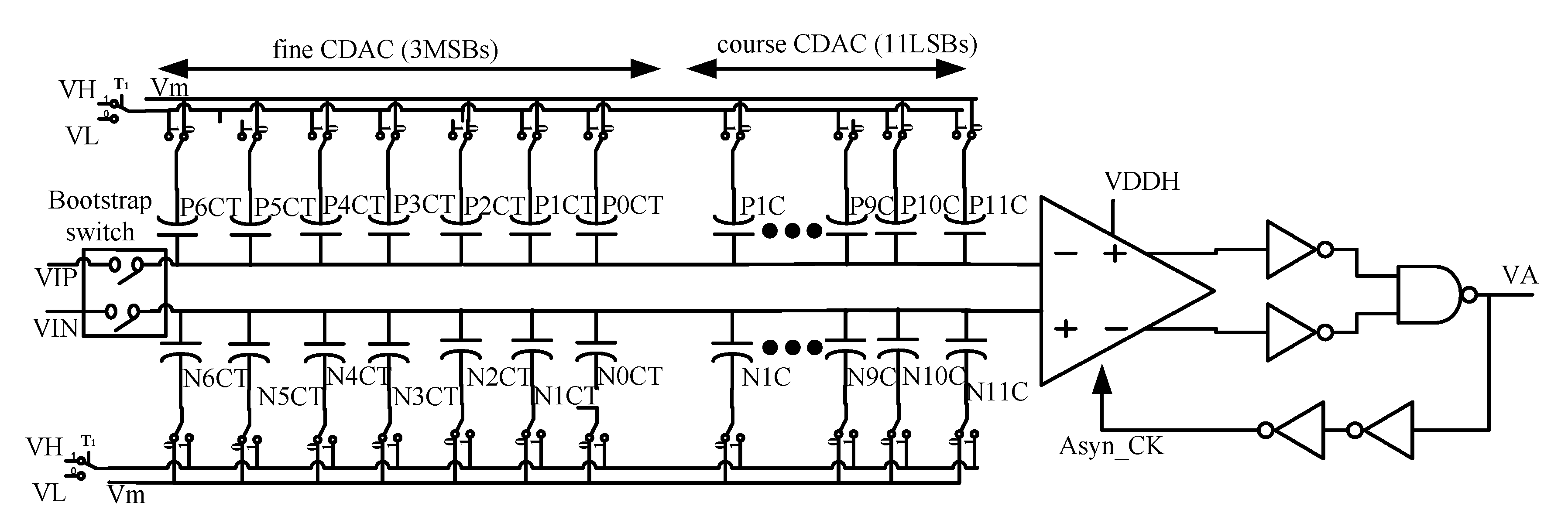
The fine conversion CDAC for the SAR-ADC-WFC-CDA contains seven capacitors. Each capacitor is 28 ƒF. The course conversion CDAC does not adopt a “radix of 2” weighted CDAC and has two additional operation cycles. Figure 3 shows the SW-B-M architecture with the fine plus course conversion CDAC.
The equations for the average switching energy of the SW-B-M are (11) and 341 Cu(VH)2. The switch numbers are 4n + 8, and the unit capacitor (Cu) number is 2 n 1 [9,10].

1.2. Non-Binary Algorithm

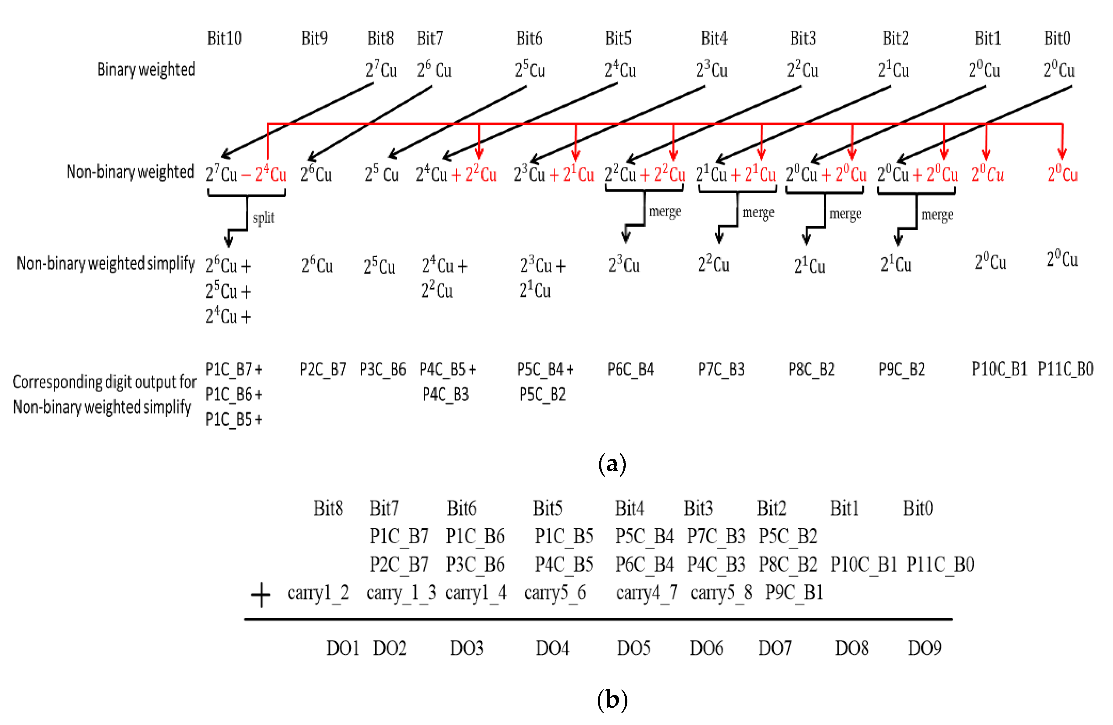
The algorithm for the binary-weighted is with “radix of 2” and the capacitance of each bit is 2 n C u , n is the bit number. The algorithm of the non-binary-weighted is not with “radix of 2” and the dispersed part of the MSB capacitor which is shown as a red-line of Figure 4a is dispersed to other bits. The number of capacitors per bit for the non-binary-weighted is split or merged to form capacitors with the radix-2 form and is renamed the non-binary-weighted simplify. The capacitors with the radix-2 form for the non-binary-weighted simplify have corresponding digital outputs and are represented by many different codes. In the 10-bit non-binary-weighted simplify, the capacitors split into ( 2 6 C u , 2 5 C u , 2 4 C u ) and the corresponding digital outputs are (P1C_B7, P1C_B6, P1C_B5). In the 9- and 8-bit non-binary-weighted simplify, the capacitor has no split, and the corresponding digital output is (P2C_B7, P3C_B6). In the 7-bit non-binary-weighted simplify, the capacitors split to ( 2 4 C u , 2 2 C u ) and the corresponding digital output is (P4C_B5, P4C_B3). In the 6-bit non-binary-weighted simplify, the capacitors keep to ( 2 3 C u , 2 1 C u ) and the corresponding digital output is (P5C_B4, P5C_B2). In the 5-bit non-binary-weighted simplify, the capacitors merge to ( 2 3 C u ) and the corresponding digital output is (P6C_B4). In the 4-bit non-binary-weighted simplify, the capacitors merge to ( 2 2 C u ) and the corresponding digital output is (P7C_B3). In the 3-bit non-binary-weighted simplify, the capacitors merge to ( 2 1 C u ) and the corresponding digital output is (P8C_B2). In the 2-bit non-binary-weighted simplify, the capacitors merge to ( 2 1 C u ) and the corresponding digital output is (P9C_B1). In the 1-bit and 0-bit non-binary-weighted simplify, the capacitors keep to 2 0 C u   and   2 0 C u and the corresponding digital outputs are P10C_B1 and P11C_B1. It extends from 9 to 11 bits and has the digital outputs of the corresponding capacitors. The corresponding digital outputs of the non-binary-weighted CDAC simplify use the error correction for the non-binary-weighted and converter 11 bits back to 9 bits, the digital outputs are DO1~DO9. In the error correction for the non-binary-weighted, P5C_B2 and P8C_B2 generate (carry5_8), P4C_B3 plus P7C_B3 generate (carry4_7), P5C_B4 plus P6C_B4 generate (carry5_6), CP1_B5 plus P4C_B5 generate (carry1_4), P1C_B6 plus P3C_B6 generate (carry1_3), and P1C_B7 plus P2C_B7 generate (carry1_2). The algorithm for the binary-weighted and the non-binary-weighted is shown in Figure 4a and the error correction for the non-binary-weighted is shown in Figure 4b.

1.3. Linearity Analysis

For the course conversion CDAC to have the same quantization error as the binary-weighted CDAC, every split capacitor must maintain the radix-2 form. The course conversion CDAC is 112 C u , 64 C u , 32 C u , 20 C u , 10 C u , 8 C u , 4 C u , 2 C u , 2 C u , C u , C u , and 112 C u split into ( 2 6 C u ,   2 5 C u ,   2 4 C u ) , 20 C u splits into ( 2 4 C u ,   2 2 C u ) , 10 C u splits into ( 2 3 C u ,   2 1 C u ) , and 2 C u splits into ( 2 1 C u ) . The fine conversion CDAC is implemented with seven capacitors of the same size ( 2 8 C u ) , and each is controlled by the conversion from binary (3 bits) to thermometer (7 bits) code. With the input code from 0,0,0 to 1,1,1, the binary-to-thermometer code changes by 1 bit in each clock cycle, and it can decrease the transient noise and improve the linearity deterioration caused by the mismatched capacitors. The benefit of having the fine conversion CDAC use the thermometer code is that it can improve the linearity and differential linearity (DNL). Because the course conversion CDAC maintains the radix-2 form, the course conversion has the same linearity and DNL as the binary-weighted CDAC [11,12].

2. The Successive Approximation Register Analog-to-Digital Converter with the Fine (Three Most Significant Bits) Plus Course Conversion (11 Least Significant Bits) Capacitive Digital-to-Analog Converter Architecture

2.1. Block Diagram of the Successive Approximation—Register Analog-to-Digital Converter with the Fine Plus Course Conversion Capacitive Digital-to-Analog Converter (SAR-ADC-WFC-CDA)

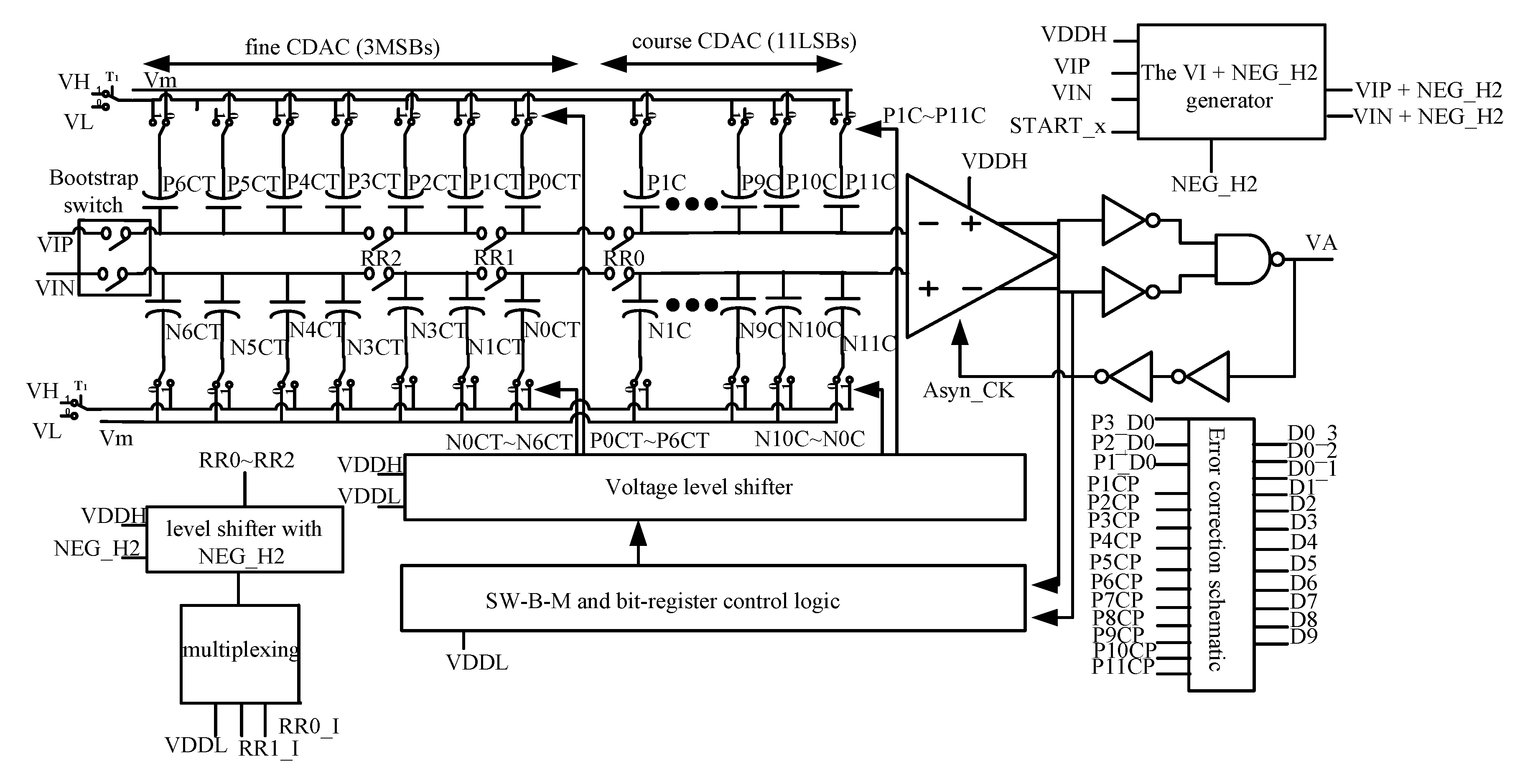
Figure 5 shows a block diagram of the SAR-ADC-WFC-CDA and is divided into analog and digital blocks. The analog block contains the bootstrap switch, two-stage comparator, SW-W-NEG (negative) and level shifter with NEG, the generator of the VI + NEG voltage, and the fine (three MSBs) plus course conversion (11 LSBs) CDAC. The digital section contains the SW-B-M and bit control logic, an internally generated clock, meta-detection, a dynamic latch, bit control logic, multi-phase control logic, fine plus course conversion switch control logic, phase control logic, and an error correction schematic. The analog and digital block use Vanalog (1.5 V) and Vdigital (0.9 V) to decrease power consumption, and the negative voltage is −1.5 V. Moreover, the RR control logic uses multiplexing and a negative voltage level shifter to generate RR0~2 through both RR (1)_I and RR(0)_I. The RR0, RR1, and RR2 control the SW-W-NEG on the upper- and lower-sides of the CDAC to divide the resolutions (9, 10, 11, and 12 bits). The power and ground for the SW-W-NEG on the upper-side of the CDAC are VDDH and VIP + Negative, and that on the lower-side is VDDH and VIN + negative. The voltage level shifter and the level shifter with NEG use contention reduction techniques to decrease power consumption and to reduce delays [13]. The unit capacitance (Cu) for CDAC is represented as 9 ƒF.

2.2. Bootstrapped Sample-and-Hold Circuit for Low-Power Application

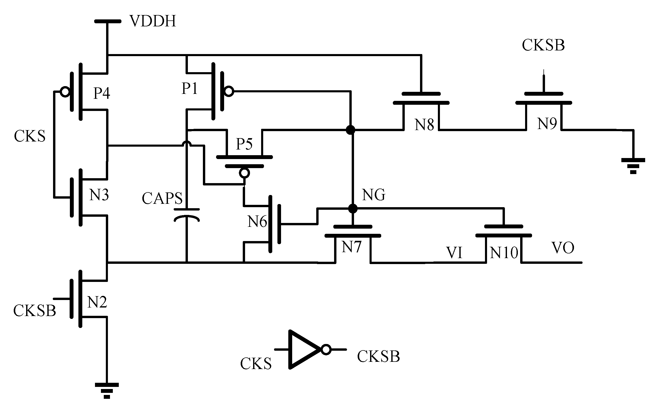
Figure 6 illustrates the bootstrap switch. When the sampling clock (CKS) pulls down to the ground (GND), the voltage of N7 (NG) is GND, and N7 and N10 are turned off. Then the top plate voltage of the CAPS is charged to the VDDH. When CKS pulls up to VDDH, the NG voltage is boosted to the voltage VDDH + VI, which is VDDH + VIP or VDDH + VIN and maintains N10 in on-resistance, which is a small constant value. The VI signal can then achieve almost the full range of the input signal and can reduce signal distortion [12]. The bootstrapped sample-and-hold (S/H) circuit is the bootstrap switch connected to the CDAC such that the total capacitors on the upper-side are 18 pf. From the transient simulation, a sample rate (fs) of the sampling clock (CKS) is 50 Ks/s, and a Nyquist input frequency (Fin) of the input signal (VI) is 25 Ks/s, fast Fourier transform (FFT) analysis takes 8192 sampling points. The dynamic performance, which is the signal-to-noise and distortion ratio (SNDR) of the S/H, is approximately 88.2 dB, and the effective number of bits (ENOBs) is approximately 14.59 bits at the typical–typical (TT) process corner and 25 °C.

2.3. Fine Conversion Capacitive Digital-to-Analog Converter Control Logic, Reconfigurable Resolution (RR) Control Logic, Switch with NEG (SW-W-NEG), and the Input Signal Plus the Negative Voltage (VI + NEG) Voltage Generator

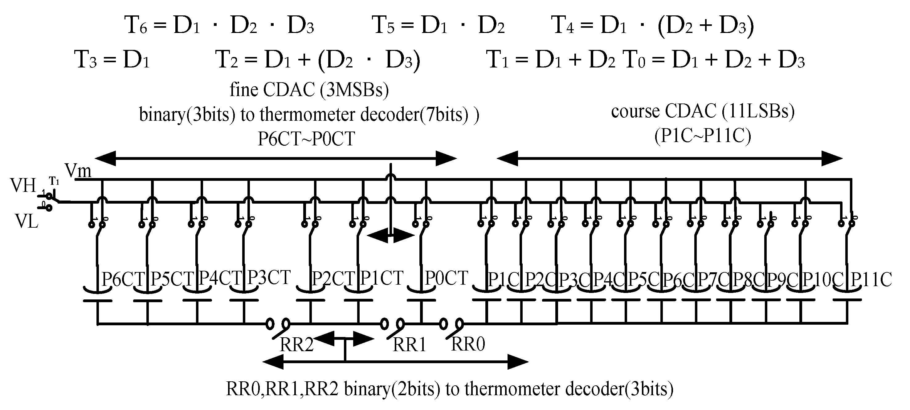
Figure 7 illustrates the fine plus course conversion CDAC and switch with NEG including RR0, RR1, and RR2. The fine conversion CDAC array uses binary (3 bits)-to-thermometer (7 bits) decoder logic to control the seven switches and seven equal 2n−4 capacitors. The RR control logic uses a binary (2 bits)-to-thermometer (3 bits) decoder to control RR0, RR0, RR2 which are the switch with NEG (SW-W-NEG) and divides the different resolutions. The binary (3 bits)-to-thermometer (7 bits) decoder logic expression is as follows.
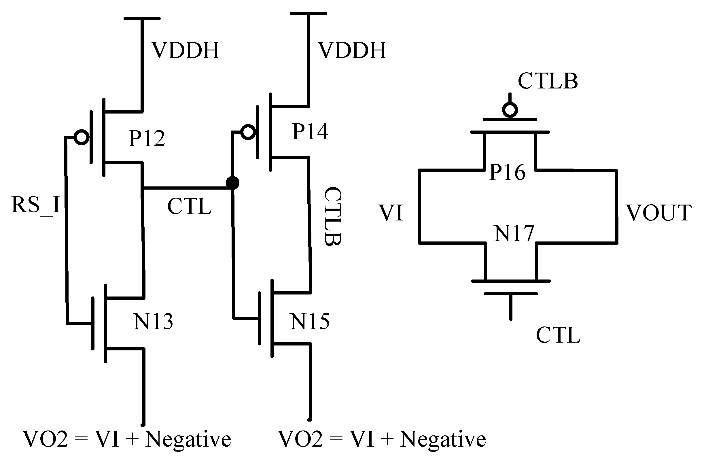
Because the SW-W-NEG uses the control signal (RR_I) to generate both CTRL and CTRL B through two inverters, which use VDDH as power and VI + Negative as ground, the SW-W-NEG has high linearity and low leakage current. Because the difference of the voltage power and ground is larger than 1.8 V, the devices of the SW-W-NEG are 3.3 V metal-oxide-semiconductor (MOS) field-effect transistors, except the SW, which is both P16 and P17, that are 1.8 V MOS, and shown in Figure 8. The parasitic capacitance of the SW has a small impact on the fine plus course conversion CDAC.
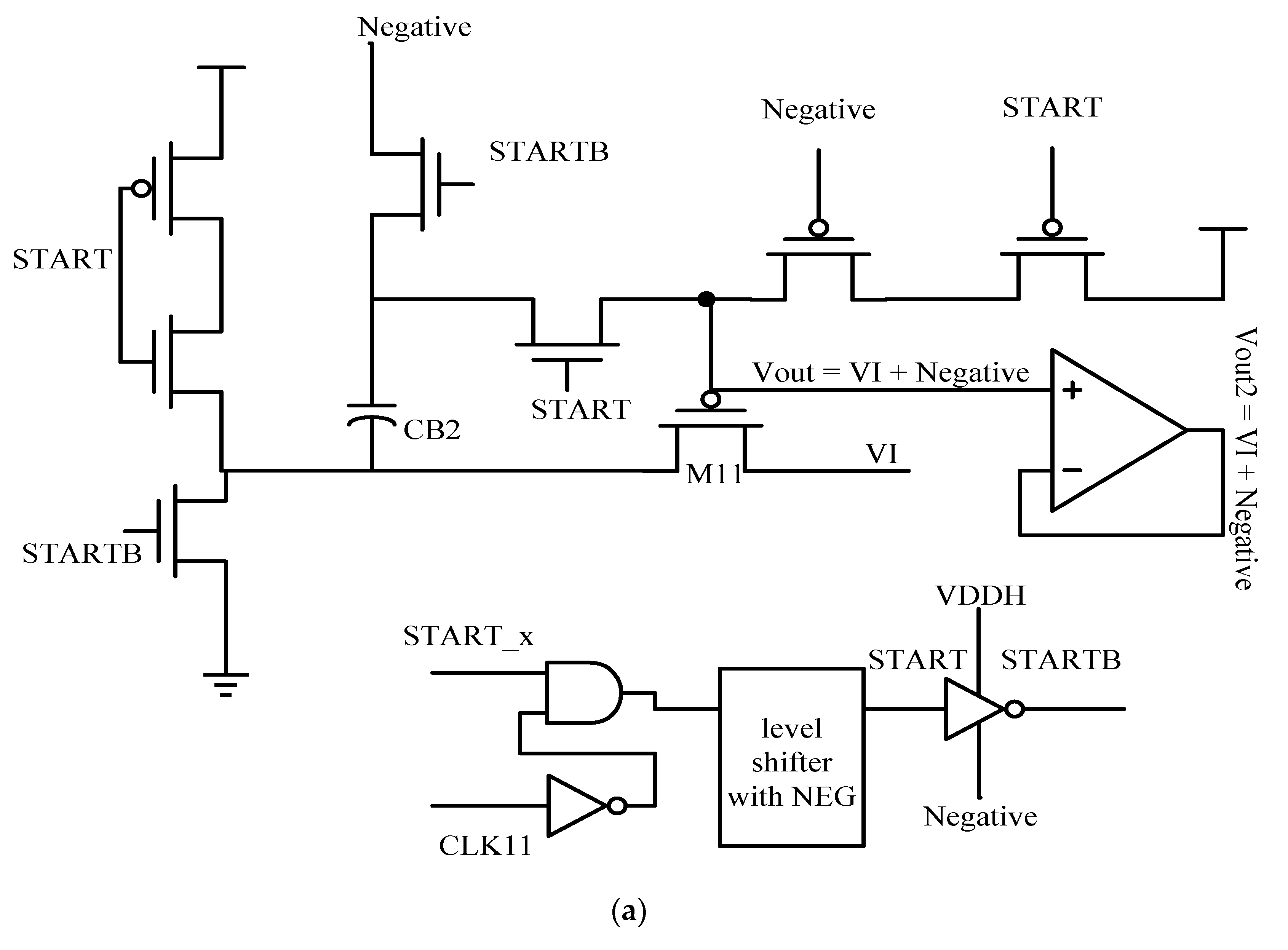
Figure 9a illustrates the VI + NEG voltage generator, which is used in the SW-W-NEG. The operation is as follows: When the START signal pulls down to GND, the top plate voltage of the CB2 is charged to the negative voltage. In Phase 2, the START signal pulls up to VDDH, and the P11 is turned on. This causes the voltage of the bottom plate of the CB2 pull to VI, which is connected from the top plate of the CDAC, and the output voltage (Vout) is boosted to VI + Negative. The Vout2 voltage, which is equal to VI + Negative, is generated through the unity gain buffer to drive the SW-W-NEG. Figure 9b illustrates the timing of START, START_x, and CLK11, which are used to control the VI + NEG voltage generator.

2.4. Internally Generated Clock, Multi-Phase Control Logic, Phase Control Logic, Fine Plus Course Conversion Switch Control Logic, Bit Control Logic, Meta-Detection, and Error Correction Schematic

The SAR-ADC-WFC-CDA uses an internal circuit to generate the internally generated clock. It does not need an extra clock generator. The internally generated clock can adjust the time of each clock period by the delay of the internal circuit and a two-stage comparator. Moreover, it adds a delay cell to increase the clock period to avoid capturing data at the CDAC unsettling time. When the differential input voltage difference of the two-stage comparator is greater than 0.5 LSB, the internally generated clock period is shorter, the CDAC settling time is shorter and leave the remaining time for the next operation cycle. When the differential input voltage difference of the comparator is less than 0.5 LSB, the internally generated clock period is longer and gives the CDAC longer settling time.
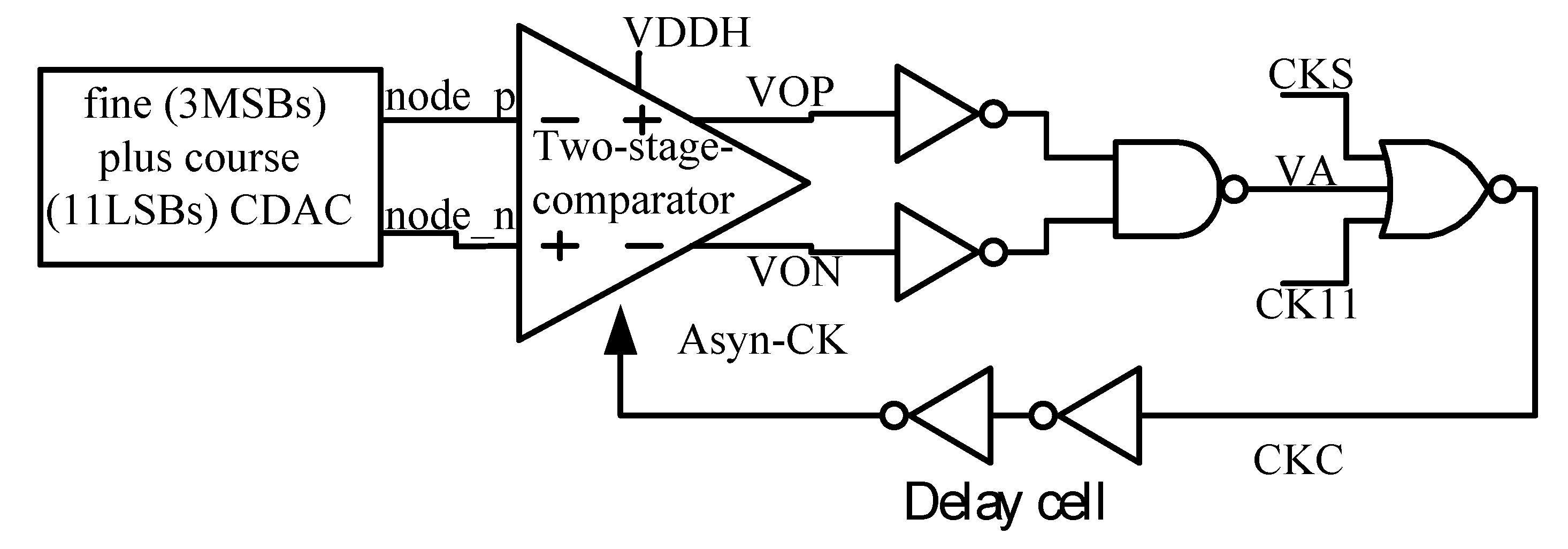
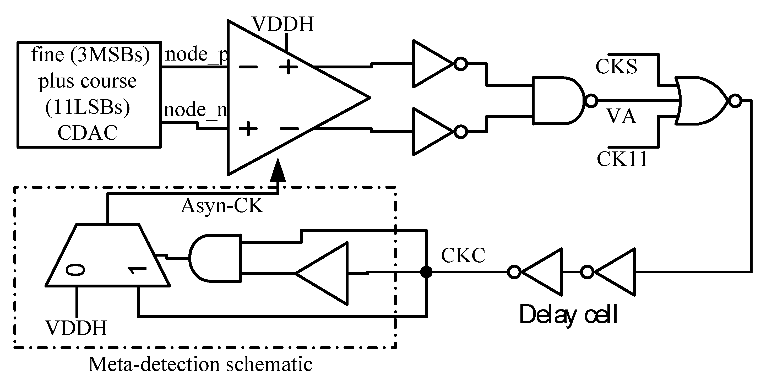
The generation procedure of the internally generated clock is as follows: The voltage at node_p and node_n passes the two-stage comparator to achieve the differential output signals (VOP and VON). The differential output signals (VOP and VON) can get a valid signal (VA) through the “INV gate” and the “NAND gate.” The CKS, CK11, and VA signal generate asynchronous clock (CKC) via the “NOR gate.” Moreover, CKC increases the clock period by the delay cell, internal circuit, and the two-stage comparator. Finally, the internally generated asynchronous clock is Asyn-CK. The procedure for the generated Asyn-CK signal is the feedback loop control. As Figure 10 indicates, the internally generated clock (Asyn-CK) is adopted to trigger the regenerative state and to reset to the initial state of the two-stage comparator.
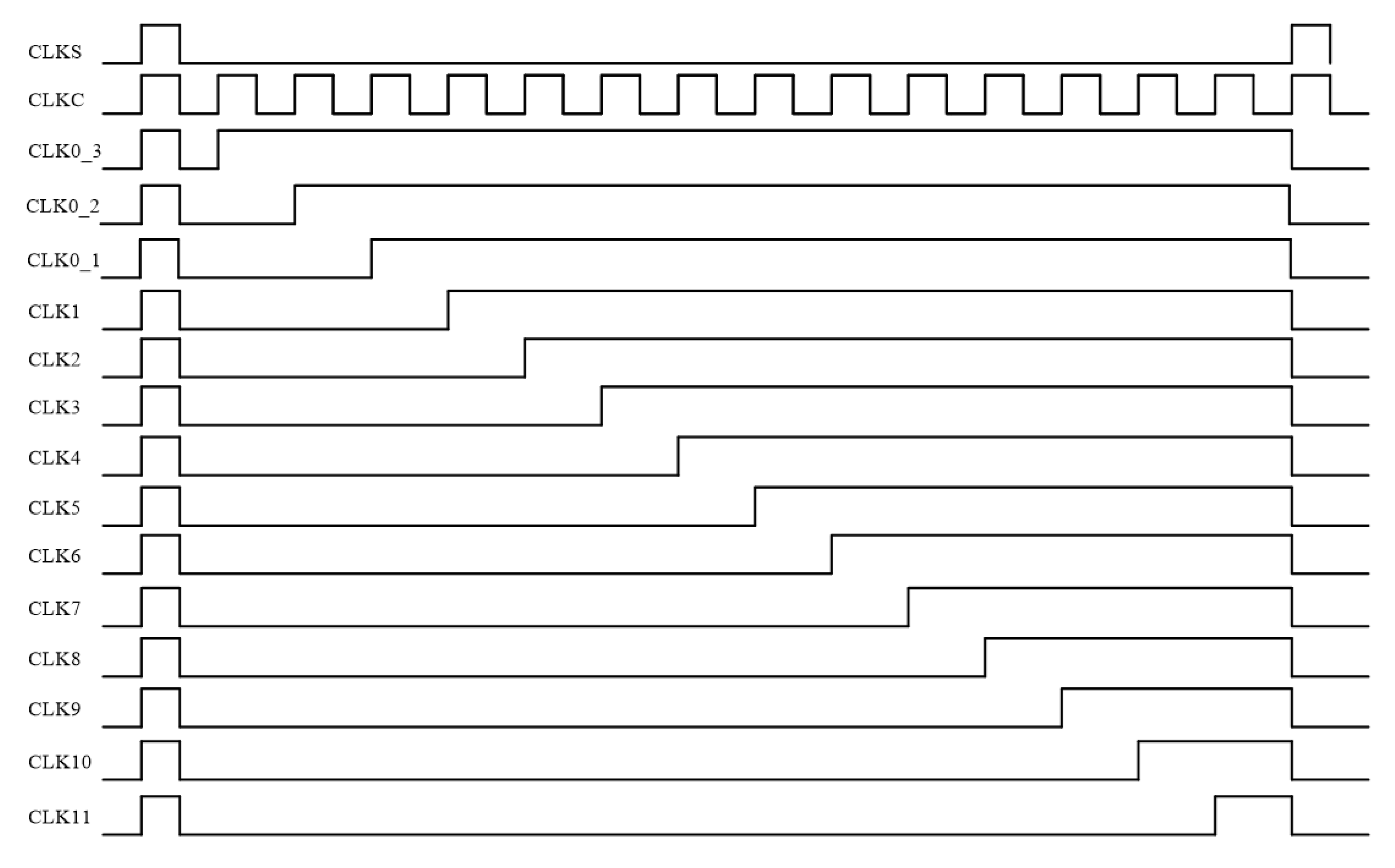
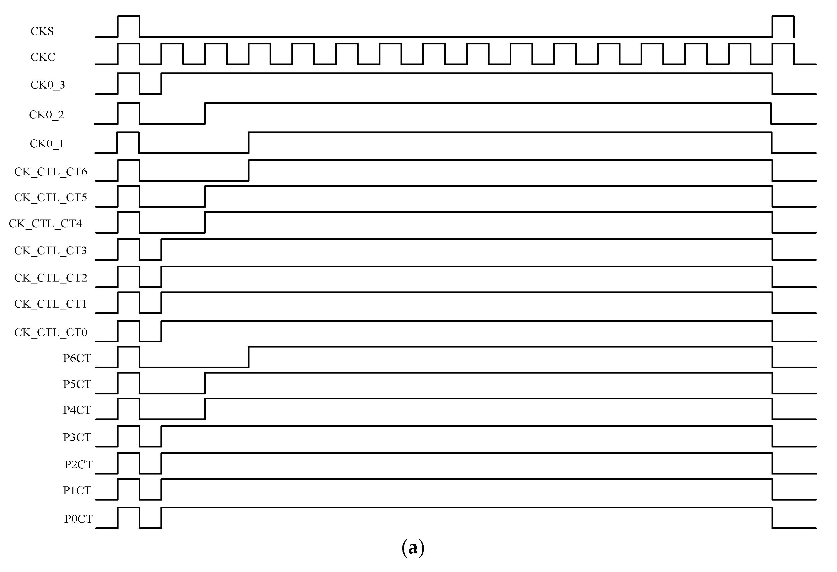
When both the CKS and the CKC are ready, the CKC signal controls the multi-phase control logic to obtain the multi-phase clock, which is CLKi. The CK11 signal is used to reset the SAR-ADC with the fine plus course conversion CDAC and reduce power consumption. Figure 11 presents the timing diagram of the multi-phase control logic and is shown with “CKi,” where “i” indicates 0_3, 0_2, and 0_1 for the fine conversion (three MSBs), and 1 to 11 for the course conversion (11 LSBs).
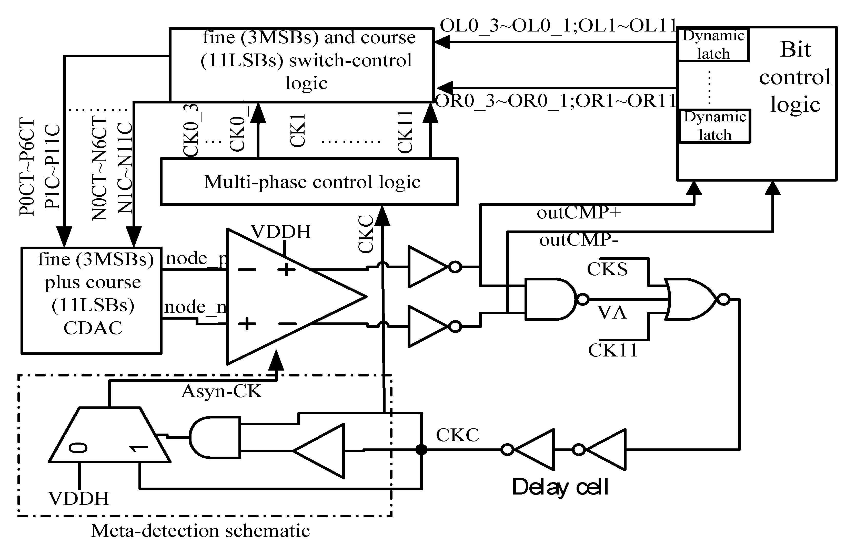
The bit control logic is the differential signals (node_p and node_n) that passes the two-stage comparator plus inverter to obtain outCMP+ and outCMP- and is triggered by the CKC. The outCMP+ and outCMP- signals are data input (Din) and connect to the bit control logic, then passes through the dynamic latch of the bit control logic to generate OL0_3~OL0_1, OL1~OL11, OR0_3~OR0_1, and OR1~OR11. Figure 12 presents a block diagram of the fine plus course conversion switch control logic, bit control logic, meta detection schematic, and multi-phase control logic.
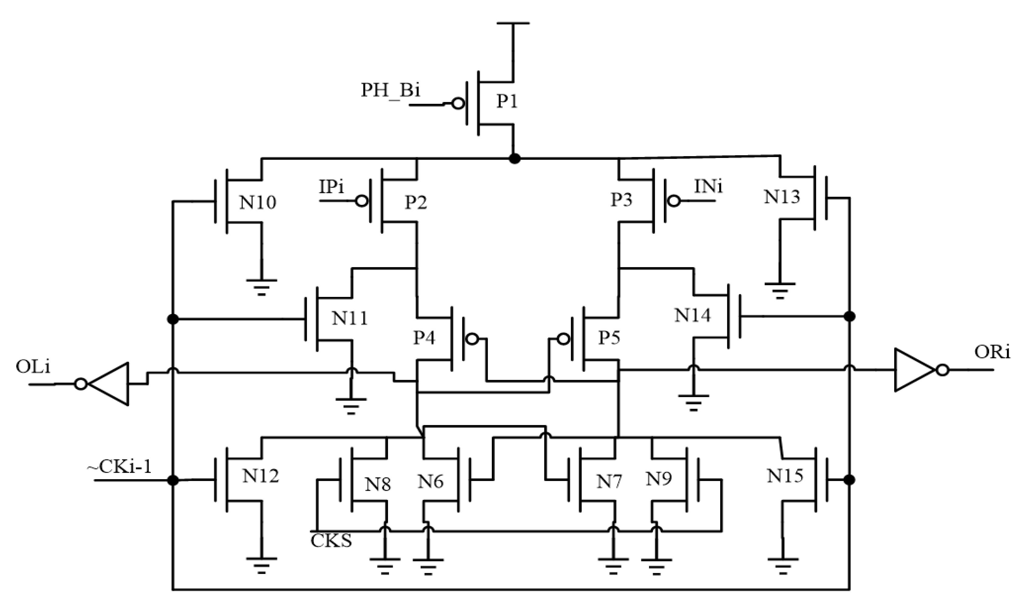
This dynamic latch is controlled by CKS, ~CKi-1, and PH_Bi and is shown in Figure 13. The dynamic latch is controlled by PH_Bi and reduces power consumption after the operation has finished. The PH_Bi is then controlled by CKS, CKi, and ~CKi-1 and is shown in Figure 14. Because the bit control logic is composed of many dynamic circuits, the data (Din) input speed increases.
As shown in Figure 12, the dynamic latch output (OLi and ORi) of the bit control logic enters the fine plus course conversion switch control logic, which is triggered by CKi to switch the specified capacitors of the CDAC. The output of the fine plus course conversion switch control logic controls P0CT to P6CT for the fine conversion CDAC on the upper-side and P1C to P11C for the course conversion CDAC on the upper-side.
The fine conversion switch control logic timing diagram for the fine conversion CDAC on the upper-side is as follows: When (CK0_3, CK0_2, CK0_1) is (0, 0, 0), (P6CT to P0CT) is (0, 0, 0, 0, 0, 0, 0), and the (P6CT to P0CT) from the Vm pulls down to VL. When (CK0_3, CK0_2, CK0_1) is (1, 0, 0), (P6CT to P0CT) is (0, 0, 0, 1, 1, 1, 1), and (P6CT to P4CT) pulls down from Vm to VL, while (P3CT to P0CT) pulls up from Vm to VH. Moreover, when (CK0_3, CK0_2, CK0_1) is (1, 1, 1), (P6CT to P0CT) is (1, 1, 1, 1, 1, 1, 1), and (P6CT to P0CT) pulls up from Vm to VH. Figure 15a shows the SW-B-M control logic timing diagram for the fine conversion CDAC array on the upper-side.
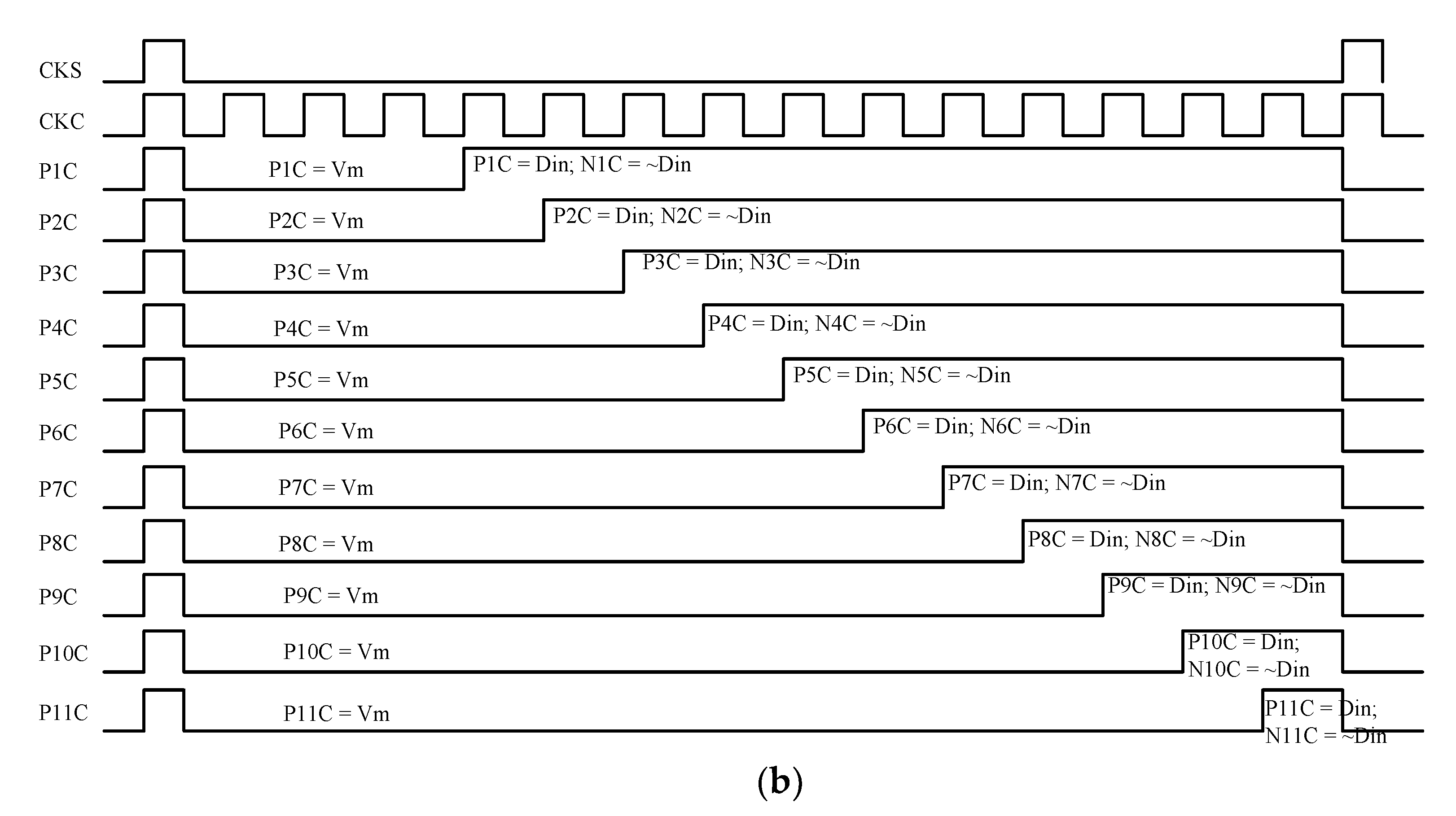
The course conversion switch control logic timing diagram for the course conversion CDAC on the upper-side is as follows: When the CKi pulls down a VL, PiC maintains Vm. Moreover, when CKi pulls up a VH, PiC is Din, and NiC is ~Din. The Din may be VH or VL. This operation is duplicated until the least significant bit of the course conversion CDAC. Figure 15b depicts the course conversion CDAC array on the upper-side.
The differential voltage (node_p and node_n) of the SAR-ADC-WFC-CDA on the top plate are changed by the capacitance ratio, which is not a factor of 2 and has two more cycles than the binary-weighted CDAC. When the external interference influences the SAR-ADC-WFC-CDA in the conversion cycle, the two additional cycles can correct the node_p and node_n voltage continuously until the n + 2 operation cycles end. Finally, the difference between node_p and node_n of the SAR-ADC-WFC-CDA should be less than 0.5 LSB.
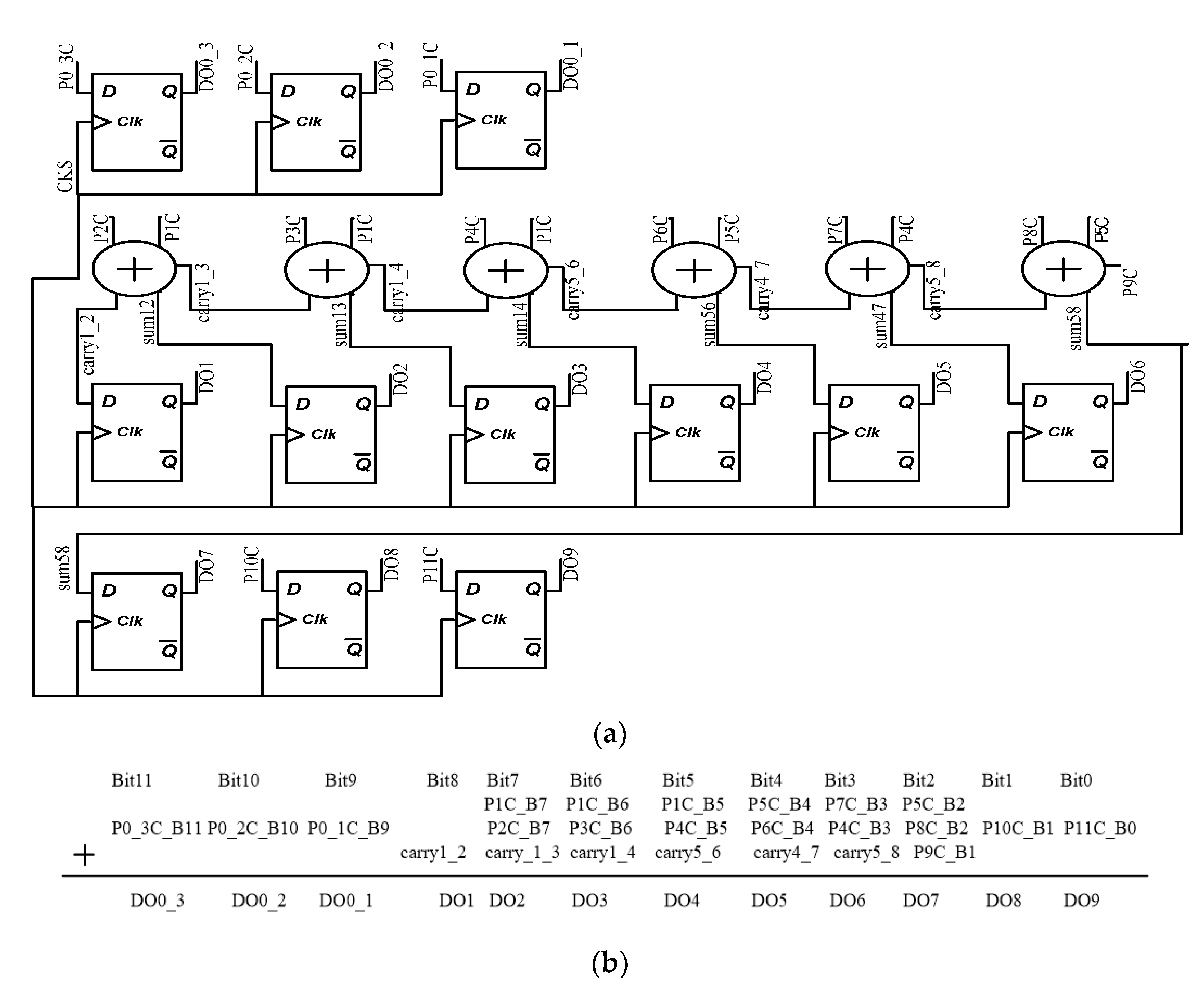
The SAR-ADC-WFC-CDA’s digital outputs are P0_3C_B11, P0_2C_B10, and P0_1C_B9 for the fine conversion CDAC. The digital outputs and algorithm for the course conversion CDAC are shown in Figure 4a,b. Through the error correction schematic algorithm for the fine plus course conversion, the digital outputs of the fine and the course conversion CDAC are integrated and convert to 12 bits, including DO0_3~DO0_1 and DO1~DO9. Figure 16a shows the error correction schematic, and Figure 16b presents the error correction schematic algorithm for the fine plus course conversion CDAC on the upper-side.
The comparator has an occasional issue with the spark code, which is a large error code. When the difference voltage of the differential input signal of the comparator is less than 0.5 LSB, it has a longer regenerative time in the bit cycle. When the regenerative time is greater than the fs and occasionally does not make a decision, the SAR-ADC-WFC-CDA digital output appears as a sparkle code. To avoid this problem, a two-stage comparator and the meta-detection schematic were designed.
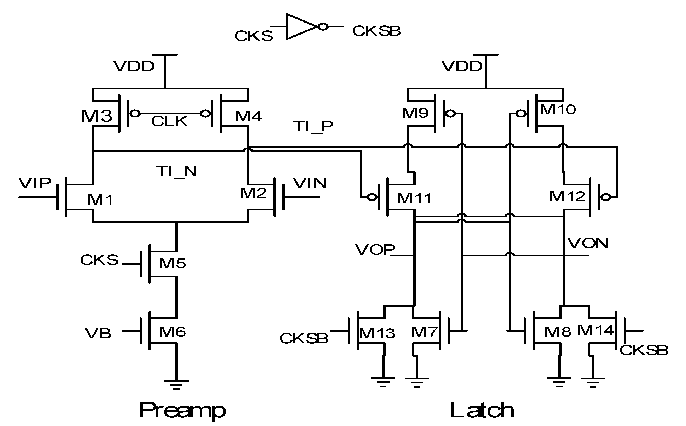
The two-stage comparator is shown in Figure 17 and the preamp magnifies the differential input voltage by 5–10 times and sends the signal to the second-stage latch, which makes the signal regenerate and reach almost full range. The input differential pair of the two-stage comparator is operated at the subthreshold region by a fixed current source (M6) to decrease the parasitic capacitance of the output of the input differential pair and to achieve low noise. The input equivalent integrated noise can be derived as Equation (12) [15]:
σ v k · T C L · 8 · V t h e r m a l V t h r e s h o l d
where k is the Boltzmann constant, V t h e r m a l is the thermal voltage, V t h r e s h o l d is the threshold voltage of the input pair transistor (M1 and M2) equal to 460 mV, and C L is the parasitic capacitance of both the TI_P and TI_N. Because the size of the input differential pair (M1 and M2) is 2 μm/0.3 μm and the parasitic capacitance of the TI_P and TI_N is less than 11 fF, the input equivalent noise is less than 0.5   LSB . The process variation effect is added into the differential pair (M1 and M2) of the two-stage comparator and uses a Monte Carlo simulation. From the Monte Carlo simulation with a typical process corner (TT) and 25 °C, the ENOB is less than 0.5 LSB, which is still in compliance with the specification.
Then the meta-detection schematic describes: From Figure 12, the Asyn-CK is formed through buffer and mux. When the voltage difference in the differential input signal of the comparator is less than 0.5 LSB, the Asyn-CK has a longer regenerative time that exceeds 4 μs and it does not make a decision. The meta-detection pulls down to a VL and Asyn-CK to a VH, which executes the two-stage comparator reset cycle. The SAR-ADC-WFC-CDA then continues to the next cycle, which includes the regenerative and reset cycles, until the end of the n + 2 clock cycles. The overall operation loses only a few cycles and maintains the remaining cycles to decrease the difference between node_p and node_n. The meta-detection method can reduce the probability of metastability. Figure 18 provides the meta-detection schematic.

2.5. Scalable Voltage Design

SAR-ADC-WFC-CDA is divided into an analog block and a digital block to decrease power consumption. The voltage level shifter is used to connect the analog and digital circuits.
The comparator regenerates the output voltage to achieve V analog · 2 n within the T d time, τ is the time constant of the comparator, T d is the time of the comparator regeneration, and g m is transconductance, as shown in Equation (13). Then, the energy of the comparator for the regenerative cycle for n + 2 conversion is represented by Equation (14).
V analog · 2 n · e ( T d τ ) = V analog ;   T d = 1 2 f s ;   τ = C L g m
I D = g m · V eff ;   E COMPreg = 2 ln 2 · ( n + 2 ) 2 · C L V eff V analog
Equations (15) and (16) show that scaling down both the Vanalog and Vdigital is effective for reducing power consumption. The analog/digital voltage is Vanalog (1.5 V)/Vdigital (0.9 V). The energy of the digital circuits for each conversion is represented by Equation (15). The load capacitance is CL (n + 2), and Vdigital is the digital block’s voltage. The energy of the comparator for each conversion, including a regenerative (ECOMPreg)–reset (ECOMPreset) cycle, is represented by Equation (16) [3,16]. The SAR-ADC-WFC-CDA needs two additional regenerative–reset cycles for each conversion, Veff is the MOS’s overdrive voltage, and the Vanalog is the analog block’s voltage. The average energy for the SW-B-M is demonstrated in Equation (11). Equations (11), (15), and (16) indicate that the average energy for the SAR-ADC-WFC-CDA increases as Vanalog and Vdigital increase.
E DIGCLK = C L ( n + 2 ) · V digital 2
E COMPreset + E COMPreg = ( n + 2 ) C L V analog 2 + 2 ln 2 · ( n + 2 ) 2 · C L V eff V analog

3. Discrete Fourier Transform-Based Calibration

X(n) is the continuous input signal, and n is the number of samples. If N samples, which are x(0), x(1), x(2), …, x(N), and each sample, x(n), is an impulse response, the Fourier transformation of the continuous input signal (x(n)) would be equivalent to:
X ( j ω ) = n = 0 N 1 x [ n ] e j ω n T = x [ 0 ] e j 0 + x [ 1 ] e j ω T + + x [ N 1 ] e j ω ( N 1 ) T = x [ 0 ] 1 + x [ 1 ] W + + x [ N 1 ] W N 1
where W = e j 2 π N and W = W 2 N = 1 .
The equation can be represented in matrix form:
[ X [ 0 ] X [ 1 ] X [ 2 ] X [ N 1 ] ] = [ 1 1 1 1 1 W W 2 W N 1 1 W N 1 W 2 ( N 1 ) W ( N 1 ) ( N 1 ) ] [ x [ 0 ] x [ 1 ] x [ 2 ] x [ N 1 ] ] Frequency   domain   Discrete   Fourier   transform   Time   domain
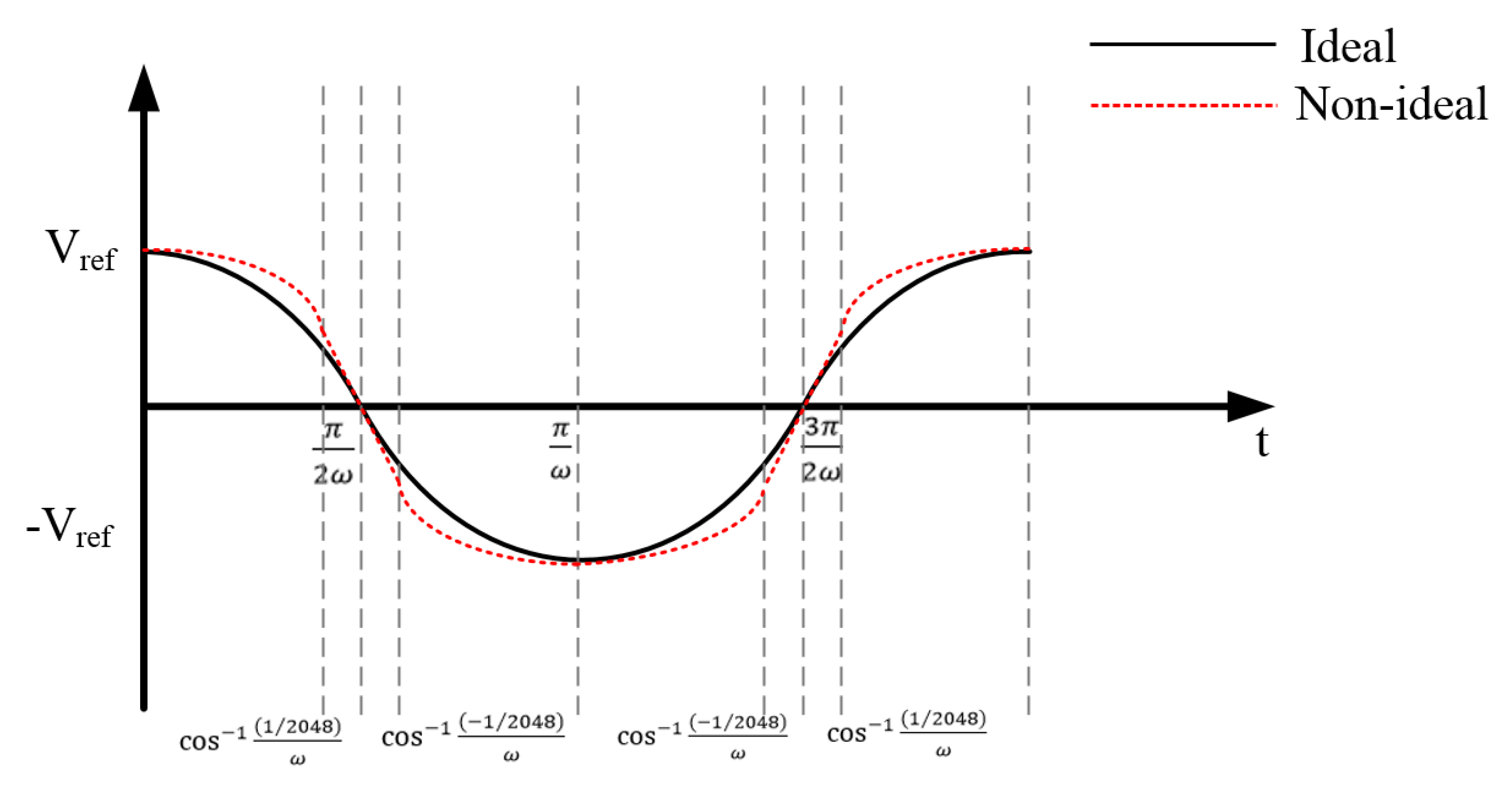
Figure 19 demonstrates the sinusoidal wave output of the SAR-ADC-WFC-CDA with the ideal signal, which is the continuous input signal, and the non-ideal signal, which is the ideal signal plus the error term of the capacitor mismatch. This matrix form shows both the frequency domain and the time domain of the continuous input signal. The DFT matrix is the corresponding matrix of the transfer from the time domain to the frequency domain. Based on References [4,17], the non-ideal signal can be modeled as V out = A cos ( ω t ) ± E , where E is the error term and is derived as follows:
E = Δ D 11 × 2 11 + Δ D 10 × 2 10 + Δ D 9 × 2 9 + Δ D 8 × 2 8 + Δ D 7 × 2 7 + + Δ D 0 × 2 0
The mismatch error from the MSB to the LSB capacitor is represented as Δ D 11 to Δ D 0 . The non-ideal corrected code is expressed below:
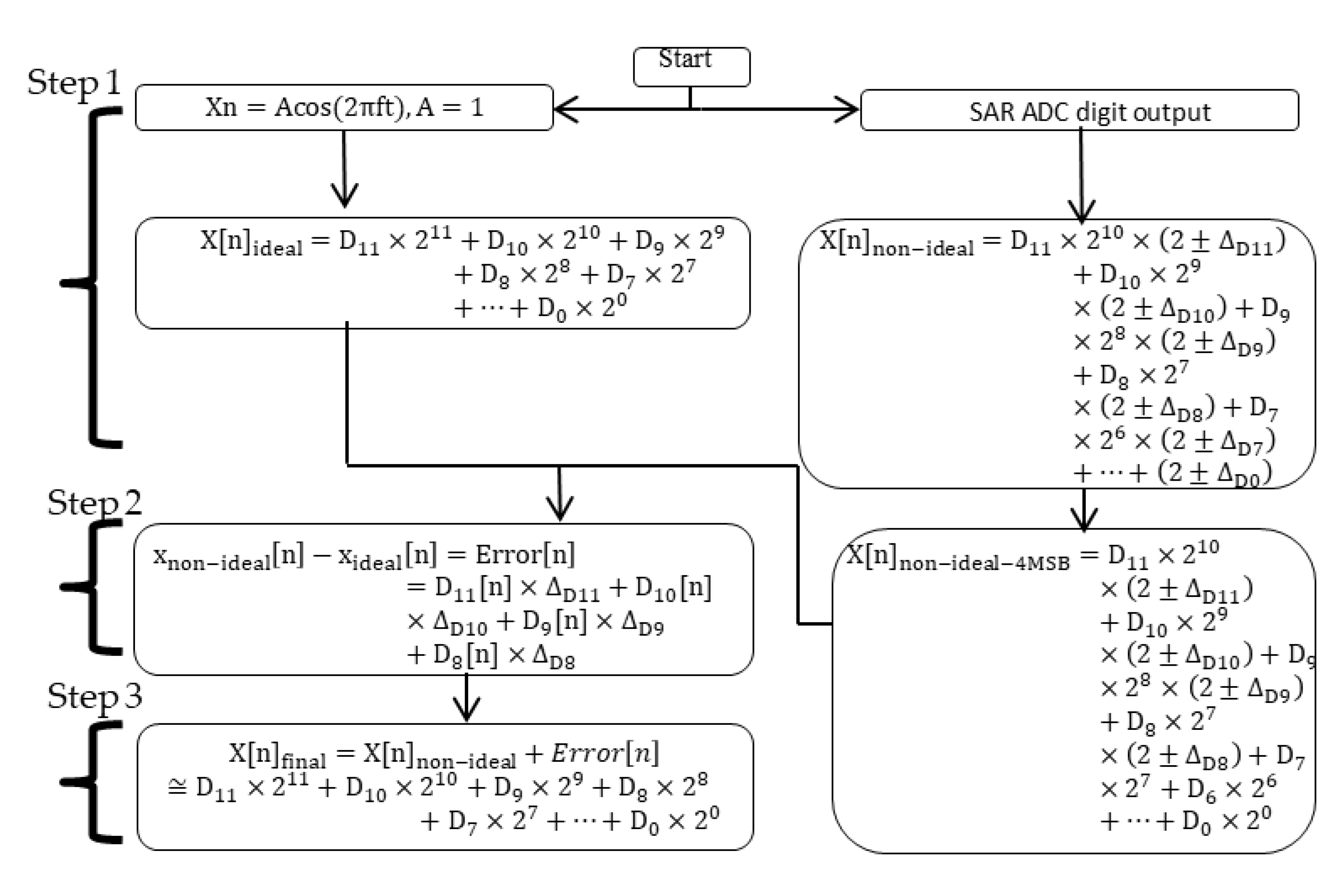
X [ n ] non ideal = D 11 × 2 10 × ( 2 ± Δ D 11 ) + D 10 × 2 9 × ( 2 ± Δ D 10 ) + D 9 × 2 8 × ( 2 ± Δ D 9 ) + D 8 × 2 7 × ( 2 ± Δ D 8 )        + D 7 × 2 6 × ( 2 ± Δ D 7 ) + + ( 2 ± Δ D 0 )
Because the four MSB capacitors are the main influence on the harmonics of the frequency response and SNDR, this study used only four compensating errors in the digital code and save memory capacity. The non-ideal corrected code for the four MSB capacitors is expressed as follows:
X [ n ] non ideal 4   MSB = D 11 × 2 10 × ( 2 ± Δ D 11 ) + D 10 × 2 9 × ( 2 ± Δ D 10 ) + D 9 × 2 8 × ( 2 ± Δ D 9 ) + D 8 × 2 7 × ( 2 ± Δ D 8 ) + D 7 × 2 7 + D 6 × 2 6 + + D 0 × 2 0
Figure 20 illustrates the DFT-based calibration procedure. The four errors are substituted in Equation (21) and are shown in step 1. Then the error term is generated by the difference between X [ n ] non ideal 4   MSB and X [ n ] ideal and is shown in step 2. Finally, the error term is added back X [ n ] non ideal to get the compensated code ( X [ n ] final ) and the compensated code is recalculated by FFT.

4. Measurement and Discussion

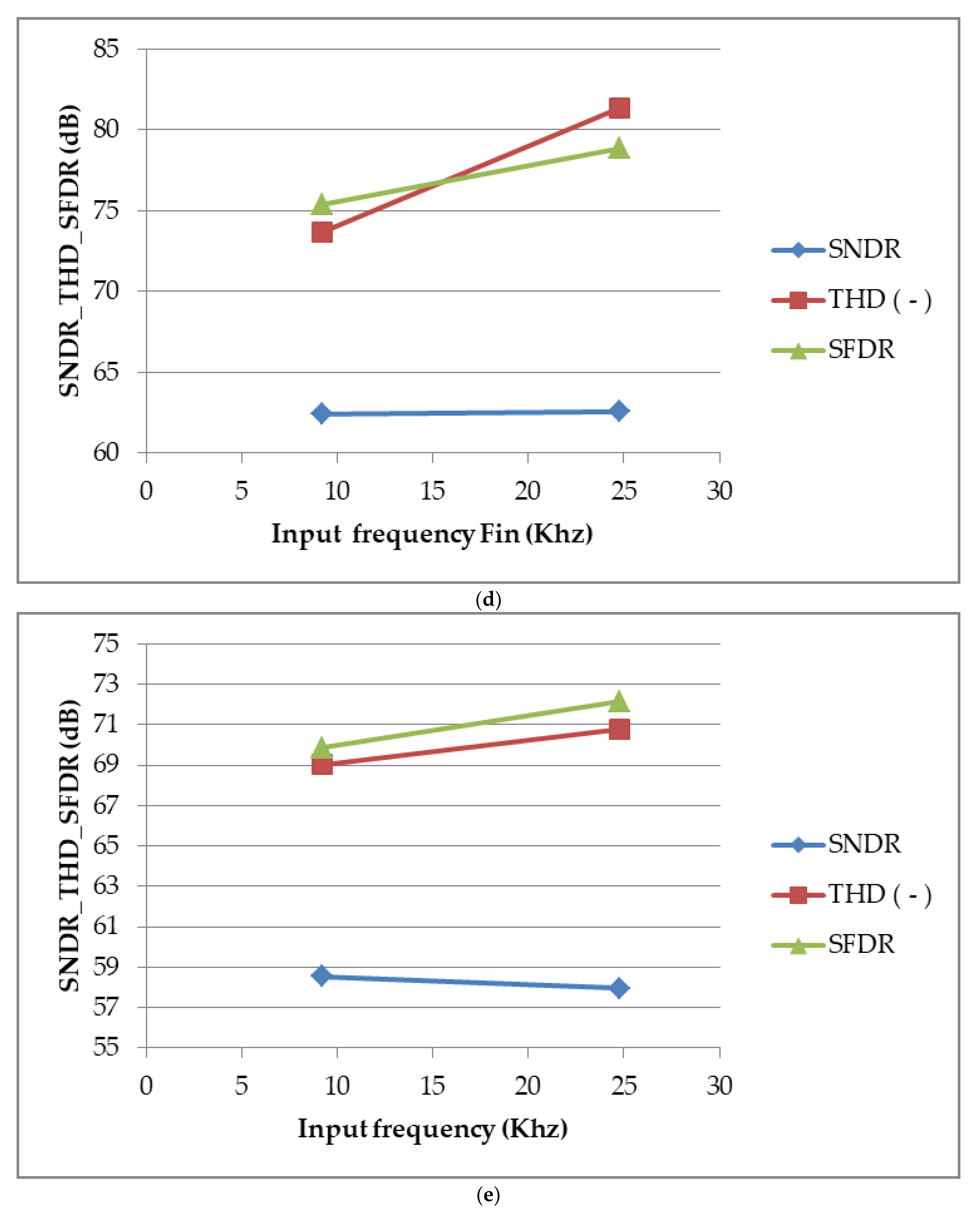
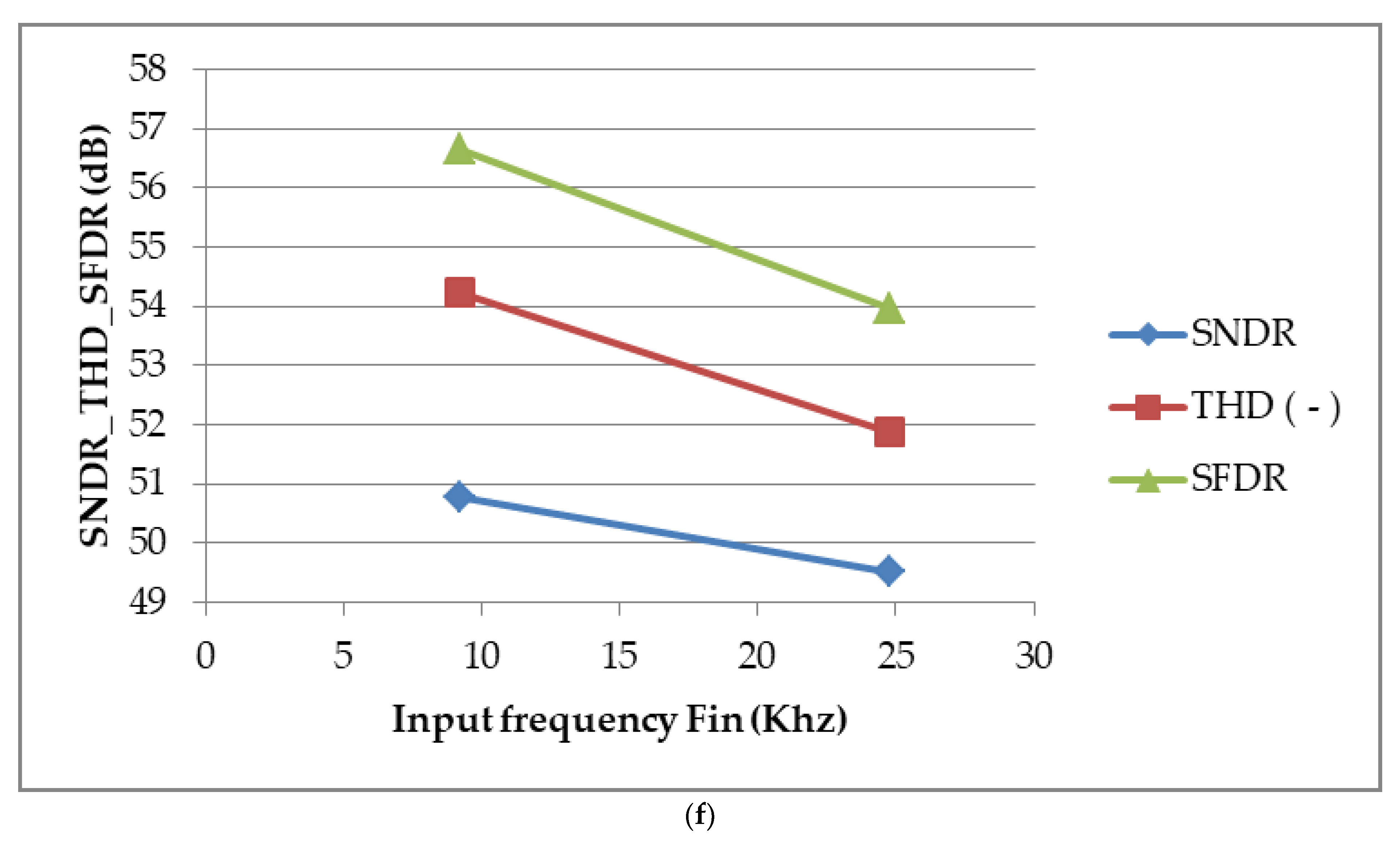
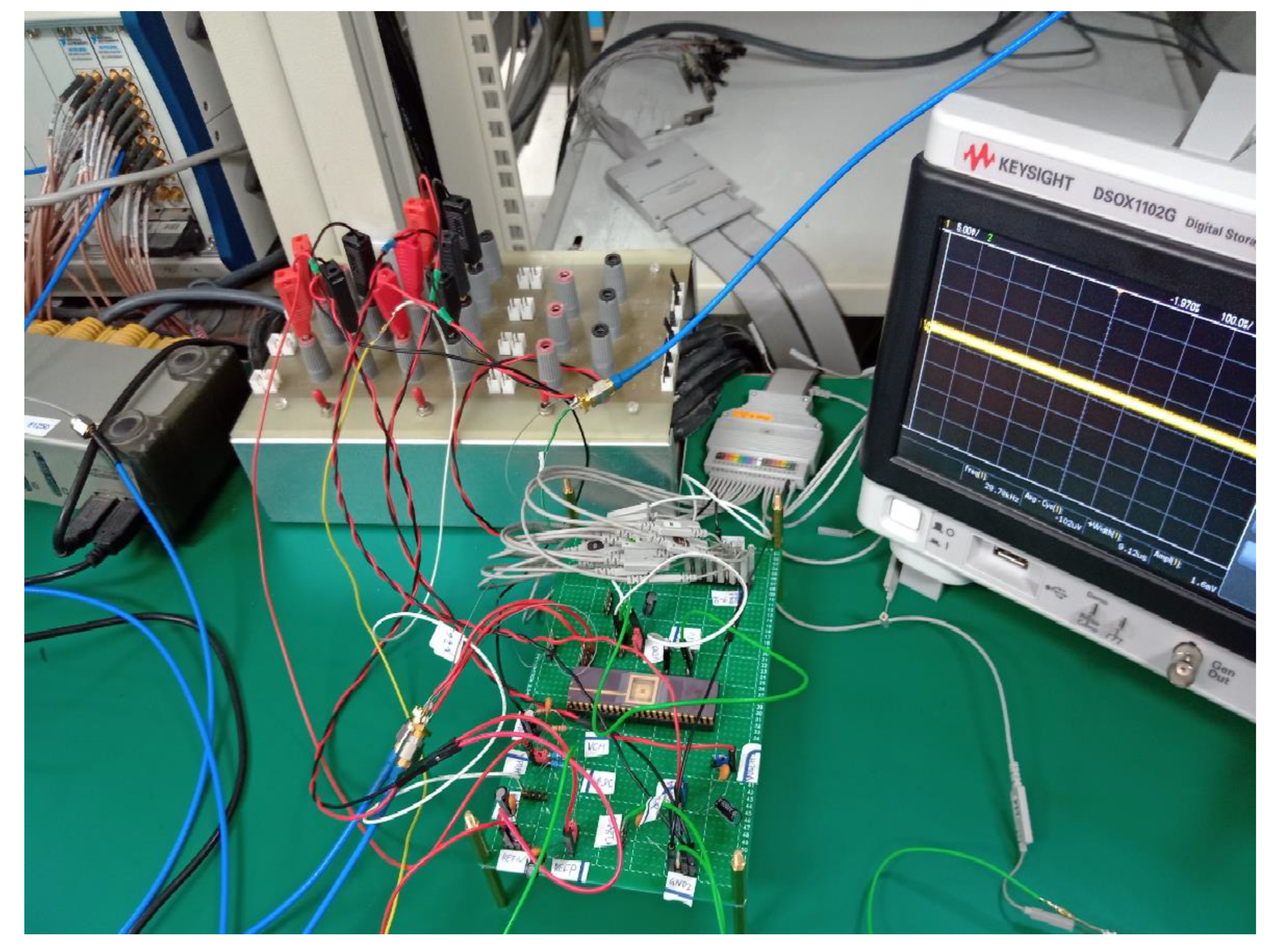
The SAR-ADC-WFC-CDA measurement results indicate the following: The Fin is 25 KS/s, which at the fs is 50 KS/s. The FFT analysis and the number of the waveform sampling points are 65,536. The analog/digital voltage is VDDH (1.5 V)/VDDL (0.9 V). The sampling clock period is 20 μs, and the duty cycle is 22%. The SAR-ADC-WFC-CDA has four reconfigurable modes (9, 10, 11, and 12 bits), and the corresponding dynamic performance (SNDR) is 50.78, 58.53, 62.42, and 66.51 dB in the 25 KS/s Fin. The figure of merit (FoM) of the 12-bit mode of the SAR-ADC-WFC-CDA is 30 fJ for each conversion step and does not calculate the VI + NEG voltage generator. In the linearity analysis, the sine wave Fin was 9.17968 KHz, the fs was 50 KHz, and 65,536 sampling points were used. The integral nonlinearity (INL) is the difference between the ideal code and the actual code and the differential nonlinearity (DNL) is the difference between two adjacent codes. The static performance was determined by the DNL and INL analysis: The DNL was approximately +0.83 LSB/−0.26 LSB, and the INL was +0.88 LSB/−0.61 LSB, as indicated in Figure 21a,b. The SNDR, total harmonic distortion (THD), spurious-Free Dynamic Range (SFDR) versus Fin for four reconfigurable modes (12/11/10/9 bits) is shown in Figure 21c–f. The SNDR, THD, SFDR, DNL, and INL data were obtained from the Taiwan Semiconductor Research Institute (TSRI). The photo of the measurement is shown in Figure 22.
Table 1 presents different successive approximation register analog-to-digital converter results, including the SAR-ADC-WFC-CDA. In these papers, the power consumption which is less than 10 uW are [1,2,3,5], while the SAR-ADC-WFC-CDA and the FOM of the SAR-ADC-WFC-CDA is lower than other papers.
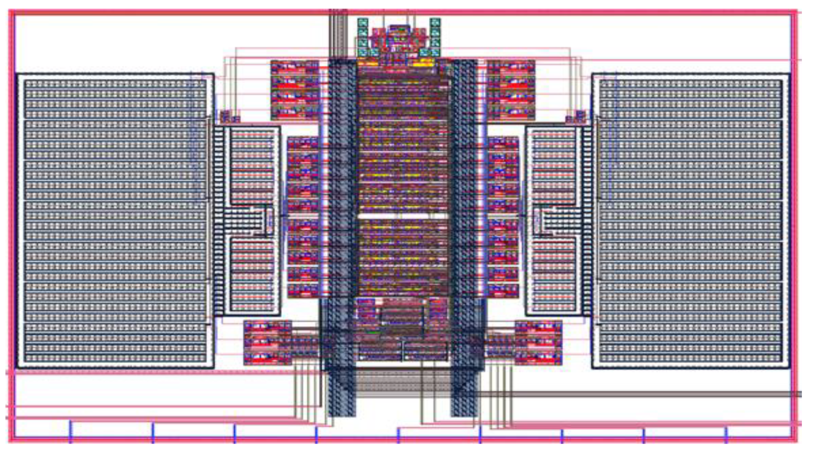
The common centroid technique was used for the layout, and extra unit capacitors were added around the CDAC to reduce the process variation effects. The layout zone is 810 × 430 μm. Figure 23 presents the floorplan for the SAR-ADC-WFC-CDA.

5. Conclusions

The SAR-ADC-WFC-CDA has a fine (three most significant bits (MSBs)) plus course conversion (11 least significant bits (LSBs)) capacitive digital-to-analog converter (CDAC) and the corresponding method is the segmented plus non-binary weighted method. The SAR-ADC-WFC-CDA includes the two-stage comparator and the bit control logic to generate data input of the fine (three MSBs) plus course (11 LSBs) conversion switch control logic, an internally generated clock to generate the multi-phase clock, fine (three MSBs) plus course (11 LSBs) conversion switch control logic to switch fine (three MSBs) plus course (11 LSBs) conversion CDAC, the bootstrapped sample-and-hold (S/H) circuit to sample and hold the input signal, a binary (2 bits)-to-thermometer (3 bits) decoder to control four-mode reconfigurable resolution (RR), the meta-detection schematic to reduce the probability of metastability, the error correction schematic to convert the output signals of the fine (three MSBs) plus course (11 LSBs) conversion CDAC to the 12 bits digital outputs.
From the measurement results, the SNDR indicates that the SNDR of the SAR-ADC-WFC-CDA was degraded by 3–5 dB for the reconfiguration solutions. The FoM of the 12-bit mode of the SAR-ADC-WFC-CDA was only 30 fJ for each conversion step and did not achieve the simulation results of 17 fJ for each conversion step. The reason is that SAR-ADC-WFC-CDA is influenced by external power noise, parasitic capacitance in the metal line, and the capacitor mismatch. The solution is to use an ultra-low-noise linear regulator to reduce the power supply noise of the power supply rejection ratio to less than −72 dB. Then, the DFT-based calibration method can be used to calibrate the SAR-ADC-WFC-CDA and to reduce the SNDR performance decline. MATLAB code was used for verification. Moreover, a comparison of the INL and DNL measurement and simulation results indicates that there was a degradation of 0.3–0.5 LSB. Moreover, the power consumptions for four reconfigurable modes (9, 10, 11, and 12 bits) were approximately 2.5, 2.66, 2.45, and 2.7 uW in the 25 KS/s Fin and can’t be reduced to meet different requirements by four reconfigurable modes. The reason for this is that the bottom plate of the CDAC is connected to Vm, is not fully floating, and continues to contribute discharge current when the fine conversion CDAC and course conversion CDAC is not in use.
The SAR-ADC-WFC-CDA has reached the specifications of the nine-axis ultra-low-power (ULP) sensing systems and the power consumptions for four reconfigurable modes are less than 10 uW. Because the SNDR, THD, and SFDR of the SAR-ADC-WFC-CDA for four reconfigurable modes are slightly worse, the FOM of the SAR-ADC-WFC-CDA can’t be further reduced. Then, the schematic of the discrete Fourier transform (DFT)-based calibration is applied to reduce the performance decline and is not included in this paper.

Author Contributions

C.-H.L. conceived the idea, designed and implemented the sensor and readout circuit SAR-ADC. K.-A.W. conceived and supervised the project. All authors have read and agreed to the published version of the manuscript.

Funding

This research received no external funding.

Institutional Review Board Statement

Not applicable.

Acknowledgments

The authors appreciate the support of UMC and TSRI, Taiwan.

Conflicts of Interest

The authors declare no conflict of interest regarding the publication of this paper.

References

  1. Aiello, O.; Crovetti, P.; Alioto, M. Fully Synthesizable Low-Area Analogue-to-Digital Converters with Minimal Design Effort Based on the Dyadic Digital Pulse Modulation. IEEE Access 2020, 8, 70890–70899. [Google Scholar] [CrossRef]
  2. Shehzad, K.; Verma, D.; Khan, D.; Ain, Q.U.; Basim, M.; Kim, S.J.; Pu, Y.; Hwang, K.C.; Yang, Y.; Lee, K.Y. Design of a Low Power 10-b 8-MS/s Asynchronous SAR ADC with On-Chip Reference Voltage Generator. Electronics 2020, 9, 872. [Google Scholar] [CrossRef]
  3. Dai, Z.; Svensson, C.; Alvandpour, A. Power Consumption Bounds for SAR ADCs. In Proceedings of the 2011 20th European Conference on Circuit Theory and Design, Linkoping, Sweden, 29–31 August 2011; pp. 556–559. [Google Scholar]
  4. Juan, Y.H.; Huang, H.Y.; Lai, S.C.; Juang, W.H.; Lee, S.Y.; Luo, C.H. A Distortion Cancelation Technique with the Recursive DFT Method for Successive Approximation Analog-to-Digital Converters. IEEE Trans. Circuits Syst. Express Briefs 2016, 63, 146–150. [Google Scholar] [CrossRef]
  5. Lin, H.M.; Lin, C.H.; Wen, K.A. A resolution-reconfigurable and power scalable SAR ADC with partial thermometer coded DAC. Adv. Sci. Technol. Eng. Syst. J. 2018, 3, 89–96. [Google Scholar] [CrossRef]
  6. Lin, H.M.; Wen, K.A. A Low Power Reconfigurable SAR ADC for CMOS MEMS Sensor. In Proceedings of the SoC Design Conference, Seoul, Korea, 5–8 November 2017; pp. 7–8. [Google Scholar]
  7. McCreary, J.L.; Gray, P.R. All-MOS charge redistribution analog-to-digital conversion techniques. IEEE J. Solid-State Circuits 1975, 10, 371–379. [Google Scholar] [CrossRef]
  8. Ginsburg, B.P.; Chandrakasan, A.P. An Energy-Efficient Charge Recycling Approach for a SAR Converter with Capacitive DAC. In Proceedings of the IEEE International Symposium on Circuits and Systems, Kobe, Japan, 23–26 May 2005; Volume 1, pp. 184–187. [Google Scholar]
  9. Lyu, Y.F. A Low Power 10-bit 500-KS/s Delta-Modulated Successive Approximation Register Analog-to-Digital Converter for Implantable Medical Devices. Master’s Thesis, Institute of Electronics, National Chiao Tung University, Hsinchu, Taiwan, 2012. [Google Scholar]
  10. Liu, C.C.; Chang, S.J.; Huang, G.Y.; Lin, Y.Z. A 10-bit 50-MS/s SAR ADC with a monotonic capacitor switching procedure. IEEE J. Solid-State Circuits 2010, 45, 731–740. [Google Scholar] [CrossRef]
  11. Tsai, J.H.; Wang, H.H.; Yen, Y.C.; Lai, C.M.; Chen, Y.J.; Huang, P.C.; Chen, H.; Lee, C.C. A 0.003 mm2 10 b 240 MS/s 0.7 mW SAR ADC in 28 nm CMOS with digital error correction and correlated-reversed switching. IEEE J. Solid-State Circuits 2015, 50, 1382–1398. [Google Scholar] [CrossRef]
  12. Haenzsche, S.; Schüffny, R. Analysis of a Charge Redistribution SAR ADC with Partial Thermometer Coded DAC. In Proceedings of the European Conference on Circuit Theory and Design, Dresden, Germany, 8–12 September 2013; pp. 1–4. [Google Scholar]
  13. Tran, C.Q.; Kawaguchi, H.; Sakurai, T. Low-Power High-Speed Level Shifter Design for Block-Level Dynamic Voltage Scaling Environment. In Proceedings of the 2005 International Conference on Integrated Circuit Design and Technology, Austin, TX, USA, 9–11 May 2005; pp. 229–232. [Google Scholar]
  14. Wang, S.; Dehollain, C. Design of a Rail-to-Rail 460 kS/s 10-bit SAR ADC for Capacitive Sensor Interface. In Proceedings of the IEEE 20th International Conference on Electronics, Circuits, and Systems, Abu Dhabi, UAE, 8–11 December 2013; pp. 453–456. [Google Scholar]
  15. Van Elzakker, M.; van Tuijl, E.; Geraedts, P.; Schinkel, D.; Klumperink, E.A.M.; Nauta, B. A 10-bit Charge-Redistribution ADC Consuming 1.9 μW at 1 MS/s. IEEE J. Solid-State Circuits 2010, 45, 1007–1015. [Google Scholar] [CrossRef] [Green Version]
  16. Yip, M.; Chandrakasan, A.P. A resolution-reconfigurable 5- to -10-bit 0.4- to -1 V power scalable SAR ADC for sensor applications. IEEE J. Solid-State Circuits 2013, 48, 1453–1464. [Google Scholar] [CrossRef] [Green Version]
  17. Lee, S.Y.; Liang, M.C.; Hsieh, C.H. FFT-based calibration method for 1.5 bit/stage pipelined ADCs. Int. J. Circuit Theory Appl. 2015, 43, 455–469. [Google Scholar] [CrossRef]
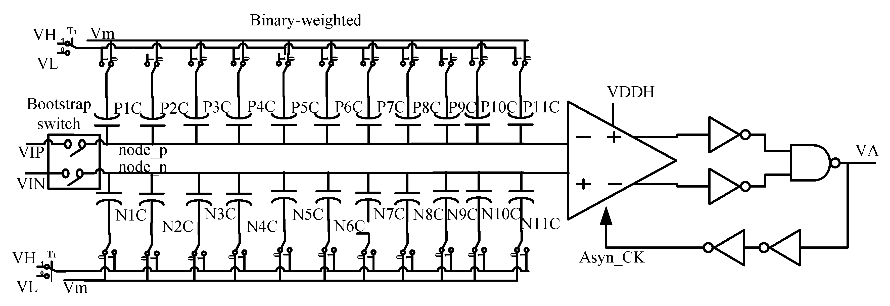
Figure 1. The switching bases midpoint voltage (Vm) (SW-B-M) architecture. VH, high-level voltage; VL, low-level voltage; Vm, midpoint voltage.
Jlpea 11 00003 g001
Figure 2. (a) SW-B-M switching procedure. (b) Waveform of the SW-B-M switching procedure. VH, high-level voltage; VL, low-level voltage; Vm, midpoint voltage; Cu, unit capacitor; VIP and VIN, input differential signals.
Jlpea 11 00003 g002
Figure 3. The SW-B-M architecture with the fine plus course conversion capacitive digital-to-analog converter (CDAC). VH, high-level voltage; VL, low-level voltage; Vm, midpoint voltage; VIP and VIN, input differential signals.
Jlpea 11 00003 g003
Figure 4. (a) Algorithm for the binary-weighted and non-binary-weighted; (b) error correction for the non-binary-weighted.
Jlpea 11 00003 g004
Figure 5. Block diagram of the successive approximation register analog-to-digital converter with the fine plus course conversion capacitive digital-to-analog converter. VH, high-level voltage; VL, low-level voltage; Vm, midpoint voltage; Cu, unit, capacitor; VIP and VIN, input differential signals; NEG_H2, negative voltage.
Jlpea 11 00003 g005
Figure 6. Bootstrap switch [14]. CKS, sampling clock; NG, boosted voltage; VI, input signal; VO, output signal.
Jlpea 11 00003 g006
Figure 7. The fine plus course conversion capacitive digital-to-analog converter and switch with NEG (RR0/RR1/RR2). VH, high-level voltage; VL, low-level voltage; Vm, midpoint voltage.
Jlpea 11 00003 g007
Figure 8. The switch with a negative voltage (SW-W-NEG) schematic. RS_I, control signal; VI, input signal; VOUT, output signal; VO2, a ground voltage.
Jlpea 11 00003 g008
Figure 9. (a) The input signal plus the negative voltage (VI + NEG) voltage generator. (b) The input signal plus the negative voltage (VI + NEG) voltage generator timing diagram. Start_x, start signal; VI, input signal; Vout, boosted voltage; Vout2, output signal.
Jlpea 11 00003 g009aJlpea 11 00003 g009b
Figure 10. The internally generated clock in the successive approximation register analog-to-digital converter with the fine plus course conversion capacitive digital-to-analog converter. CKS, sampling clock; CK11, the last multi-phase clock.
Jlpea 11 00003 g010
Figure 11. The multi-phase control logic timing diagram.
Jlpea 11 00003 g011
Figure 12. Block diagram of the fine plus course conversion switch control logic, bit control logic, meta-detection schematic, and multi-phase control logic.
Jlpea 11 00003 g012
Figure 13. Dynamic latch.CKS, sampling clock; PH_Bi, the control signal; CKi; the i-th multi-phase clock; IPi and INi, the input differential signals; OLi and ORi, the dynamic latch output signals.
Jlpea 11 00003 g013
Figure 14. Phase control logic. CKS, sampling clock; PH_Bi, output signal; CKi; the i-th multi-phase clock.
Jlpea 11 00003 g014
Figure 15. (a) Fine conversion switch control logic timing diagram for the fine conversion capacitive digital-to-analog converter on the upper-side. (b) Course conversion switch control logic timing diagram for the course conversion capacitive digital-to-analog converter on the upper-side. Din, input data.
Jlpea 11 00003 g015aJlpea 11 00003 g015b
Figure 16. (a) Error correction schematic for the fine plus course conversion capacitive digital-to-analog converter. (b) Error correction algorithm for the fine plus course conversion capacitive digital-to-analog converter on the upper-side. CKS, sampling clock.
Jlpea 11 00003 g016
Figure 17. Two-stage comparator. CKS, sampling clock; VB, a fixed voltage.
Jlpea 11 00003 g017
Figure 18. The meta-detection schematic. CKS, sampling clock; CK11, the last multi-phase clock.
Jlpea 11 00003 g018
Figure 19. The successive approximation register analog-to-digital converter with fine (3 MSBs) plus course (11 LSBs) capacitive digital-to-analog converter sinusoid wave output with the ideal signal and the non-ideal signal.
Jlpea 11 00003 g019
Figure 20. Discrete Fourier transform-based calibration procedure.
Jlpea 11 00003 g020
Figure 21. (a) The differential linearity of the SAR-ADC with the fine plus course conversion capacitive digital-to-analog converter. (b) Integral linearity of the SAR-ADC with the fine plus course conversion capacitive digital-to-analog converter. (c) SNDR, THD, SFDR versus Fin for the 12-bit mode of the SAR-ADC with the fine plus course conversion capacitive digital-to-analog converter. (d) SNDR, THD, SFDR versus Fin for the 11-bit mode of the SAR-ADC with the fine plus course conversion capacitive digital-to-analog converter. (e) SNDR, THD, SFDR versus Fin for the 10-bit mode of the SAR-ADC with the fine plus course conversion capacitive digital-to-analog converter. (f) SNDR, THD, SFDR versus Fin for the 9-bit mode of the SAR-ADC with the fine plus course conversion capacitive digital-to-analog converter.
Jlpea 11 00003 g021aJlpea 11 00003 g021bJlpea 11 00003 g021cJlpea 11 00003 g021d
Figure 22. The photo of the measurement.
Jlpea 11 00003 g022
Figure 23. The successive approximation register analog-to-digital converter with the fine plus course conversion capacitive digital-to-analog converter layout.
Jlpea 11 00003 g023
Table 1. Successive approximation register analog-to-digital converter results. Fs, sampling rate; SNDR, signal-to-noise and distortion ratio; FoM, figure of merit.
[3][4][5][1][2]SAR-ADC-WFC-CDA
Resolution10 bits12 bits12 bits6.4 bits6.7 bits12 bits9/10/11/12 bits
Process0.13 μm0.18 μm0.18 μm0.04 μm0.04 μm0.055 μm0.18 μm
Analog, digital1.0 V, 0.4 V1.8 V, -1.8 V, 0.9 V-, 1.0 V-, 0.6 V1 V, 1 V1.5 V, 0.9 V
Layout zone0.19 mm22.38 mm20.35 mm23000 μm24970 μm20.039 mm20.052 mm2
Fs1 KS/s200 KS/s50 KS/s2.8 KS/s2.2 KS/s1 MS/s50 KS/s
SNDR56.54 dB69.6 dB68.6 dB40.4 dB42.1 dB59.3 dB50.78/58.53/62.42/66.51 dB
Power0.05 μW41.5 μW9.7 μW7.3 uW0.94 uW108uW–/–/–/2.7 μW
FoM94.5 fJ/conversion84.6 fJ/conversion88.4 fJ/conversion30,900 fJ/conversion4110 fJ/conversion17.8/conversion–/–/–/30.5 fJ/conversion
Publisher’s Note: MDPI stays neutral with regard to jurisdictional claims in published maps and institutional affiliations.