1. Introduction
The 0.25 µm FEOL (front end of line) technology node was the first to replace the LOCOS (local oxidation; see, e.g., [
1]) integration scheme with shallow trench isolation (STI). The three main reasons for that were as follows:
There was a need for a reduction in spacing between devices. However, due to the formation of the bird’s beak, the conventional LOCOS isolation structure does not scale well.
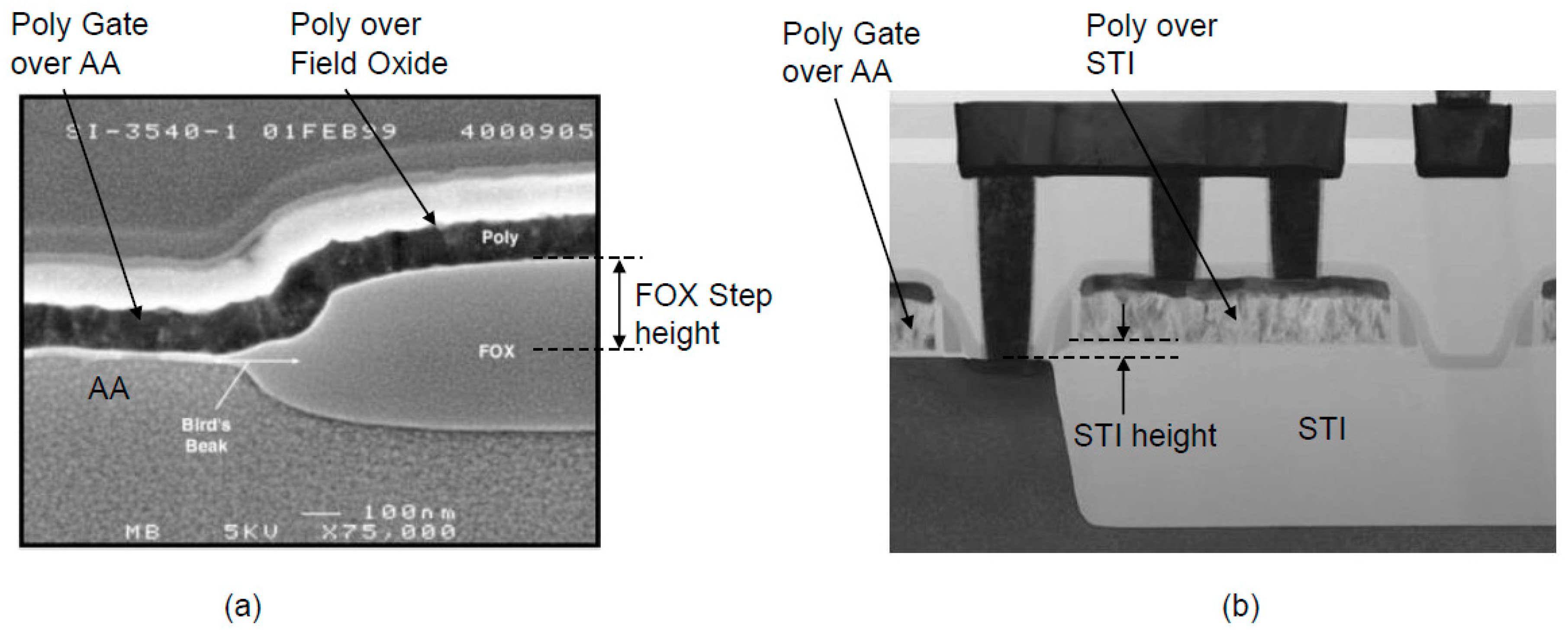
Limited depth of focus (DOF) for the gate patterning, due to the relatively large step height of the field oxide above the active area (AA) surface (
Figure 1a).
Stresses from the nitride layer over the pad oxide induced dislocations into the silicon and led to junction leakage.
These limitations enhanced the STI integration development (
Figure 1b): a shallow trench is etched into the silicon substrate and then filled with a deposited oxide. The surface is then planarized by CMP (chemical mechanical polishing) to complete the isolation structure. By this integration scheme, the three limitations listed above are minimized.
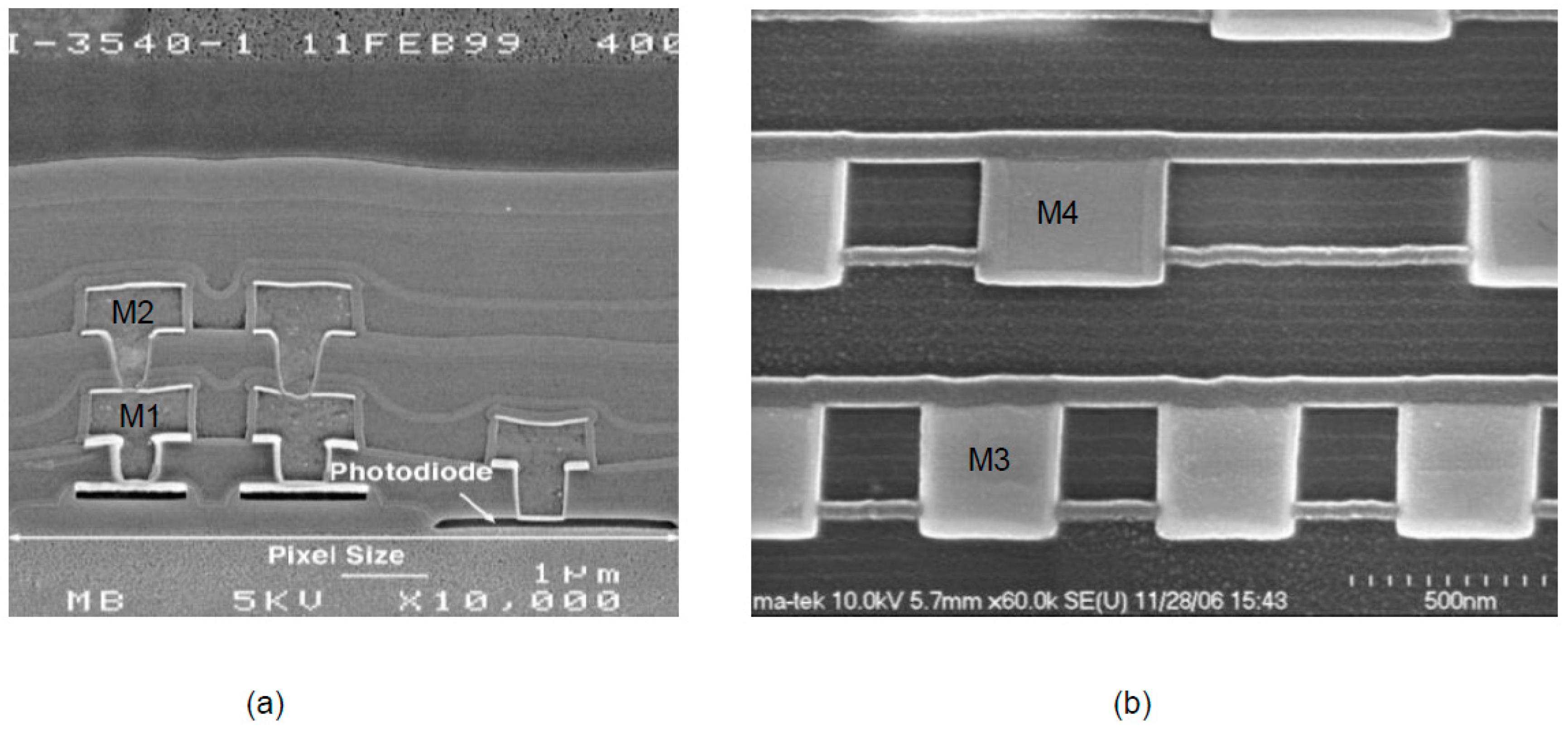
The 0.35 μm BEOL (back end of line) was the first technology that implemented CMP for dielectric planarization with Al metal lines. The 0.13 µm technology node was the first that replaced the Al interconnect (
Figure 2a) with planarized Cu (
Figure 2b). The two main reasons for that were as follows:
Limitation of the circuit performances due to high resistance capacitance (RC) delay. Along the scaling path, the minimum metal line width was reduced by a factor of ≈0.7 from generation to generation to maintain high density, and the line thickness was reduced by a similar factor to avoid the high aspect ratio, which might cause gap fill issues. The result was higher line resistance. The advantage of using Cu is the lower bulk resistivity compared to Al (approximately 40% lower), together with superb electromigration (EM) performance.
The reduction in the interconnect cross-section area along the scaling reduced the maximum current density (Jmax), which was limited due to EM. For the same temperature and cross-section area, a Cu line can handle Jmax > 3.5 times that of Al.
In Cu integration, the intermetal dielectric (IMD) layer is first patterned and etched and is then filled with Cu. The surface is then fully planarized by CMP to complete the interconnect formation (
Figure 2b).
To achieve good CMP planarization, the coverage of the material to be polished should be within certain limits. The term “coverage” refers to the pattern density, that is, the percentage of material at a certain checking window; a more detailed definition is provided later. When the design has a low coverage, dummy features of the material to be polished are inserted manually or by automatic insertion thus increasing the coverage. The insertion methods are also discussed in detail in this paper.
The examples shown in
Figure 2 are formed with oxide or Cu CMP processes. However, advanced technologies also require Al-CMP. At the 28 nm technology, Poly/SION for gate structures was used for the last time for low power (LP) applications. The same technology was also used in High-k/Metal Gate (HKMG) for applications such as high performance for mobiles (HPM). The most popular integration for 28HPM is gate-last that consists of replacement of the poly gate and the gate oxide underneath with HKMG. This replacement of metal gate (RMG) takes place after interlayer-dielectric (ILD) planarization, prior to the contact module. Afterwards, the metal gate trench is filled with low-resistance Al followed by Al-CMP. Intel used the same integration for 45 nm technology [
2].
Precise control of the gate height and gate height uniformity is a primary challenge for the HKMG Al-CMP process. Beyond the DOF limitation, non-uniform gate height can cause gate resistance variation, and improper gate heights can result in contact etch problems. In CMOS platforms prior to Al-CMP integration (e.g., 45 nm technology), the gate height is approximately 60 nm. Such a large gate height strongly affects the transistor performance. Researchers from UMC [
3] learned the affect of the metal gate area and pattern density on gate height loss due to Al dishing: The loss increases with increasing metal gate area and pattern density. Adding dummy gate lines reduced the gate height loss. Based on their study, we can set a simple design rule (DR), i.e., at least one (recommended two) dummy poly line is needed at both sides of each metal gate to effectively reduce metal gate height loss. In addition, optimized dummy metal gate structures are needed to reduce variability.
The insertion of dummy features increases the coverage and improves the coverage uniformity across the die and the wafer. With regard to the dummy fill insertion methods and utilities developed for technology scaling, a previous study [
4] shows that for 180 nm technologies down to 90 nm technologies, in most cases, dummy insertion is based on a single size dummy feature. Afterwards, based on some basic elimination rules, some of the dummies are removed. At the scale of 65–40 nm technologies, and mostly for Cu BEOL, the fill insertion was based on “analysis-driven fill”—each local window in the design is filled based on the local coverage and the gradient coverage to the neighbors around (explained later in this paper). A cell-based fill was introduced for the 28 nm platforms by leading IC manufacturers. The cell is composed of several layers, with a pattern matching that of a transistor (e.g., for AA and poly coverage) and a net grid for BEOL. This method is also explained later in this paper. The most recent fill insertion run-sets for 20 nm technologies and below also handle double or triple patterning (DP/TP). For 16 and 10 nm technology, the cell-based fill’s target is to maximize the insertion efficiency for better uniformity. The insertion takes into consideration the tight alignment requirements of the tile to the fins, DP integration, voltage-aware design, and more. All these topics are explained in detail in this review. Finally, <28 nm technology, engineering change orders (ECO) for design fixes become increasingly complicated due to the heavy duty of the dummy fill. This is also discussed herein.
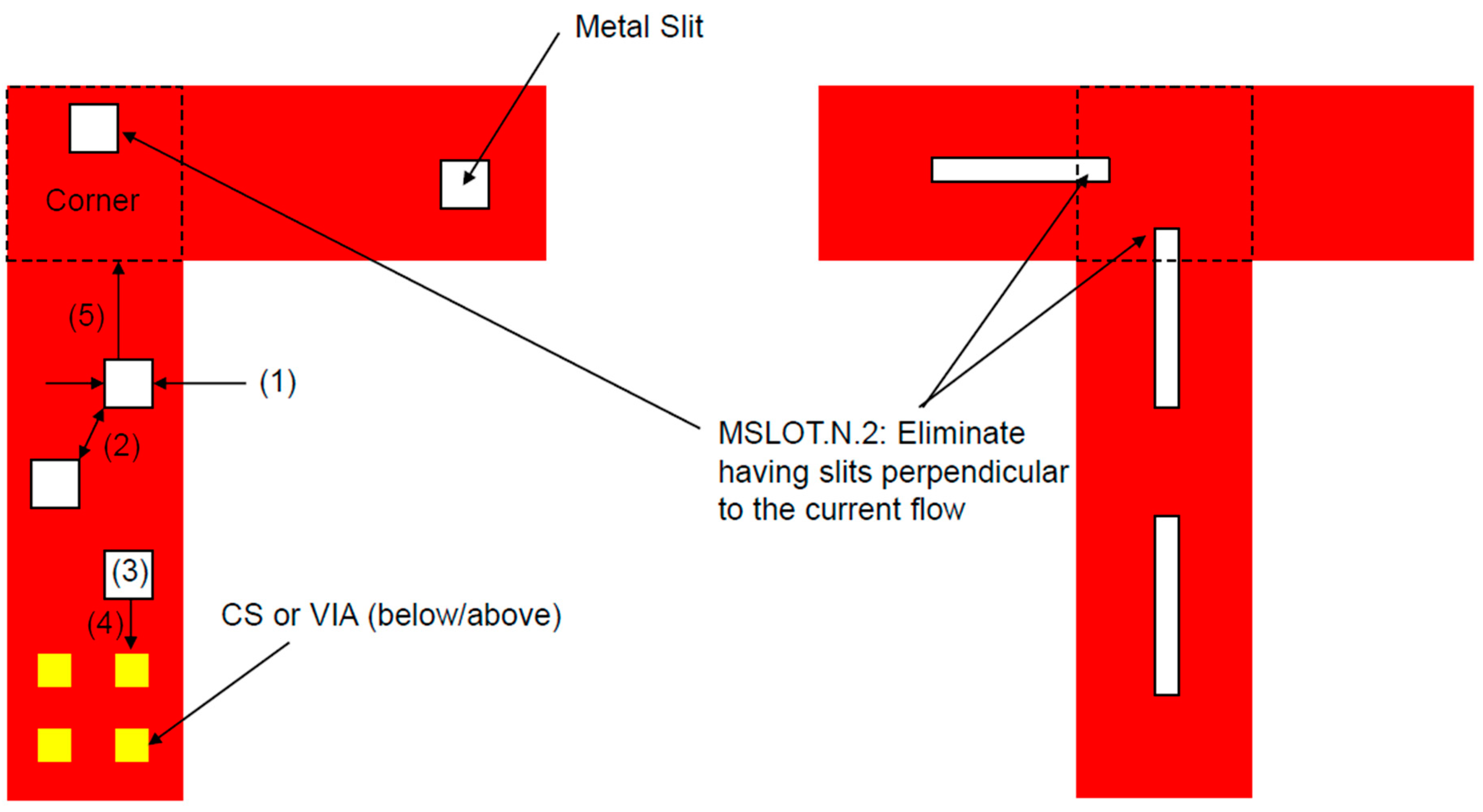
This review paper is organized as follows: first, the dependency of CMP and reactive ion etch (RIE) processes on the patterning coverage will be discussed. Next, an explanation for different local coverage rules will be given with many examples for the reason and the sensitivity of each rule. Several methods for dummy fill insertion will be presented, i.e., single-size, rule-based, and model-based, along with the special care required for filling near a net wire. Finally, metal slits rules will be explained. The aim of this review is to provide the typical foundry and leading IC manufacturer’s perspective for coverage layout rules and the supported utilities. For this review, we used published data from foundries and leading integrated device manufacturers (IDMs), together with our own experimental process and device characteristics accumulated over the years.
2. CMP Process Integration
In a CMP process, the wafer being planarized is pressed face down on a polymer-based pad and is polished with a slurry that contains both active chemicals and abrasive particles. In general, the process of removing material from the wafer surface is based on a combination of both the mechanical energy induced by the polish head and abrasives and the chemical reaction from the slurry.
2.1. CMP Planarization for Oxide and Cu
The local polish rate has a strong dependency on the feature’s pattern density.
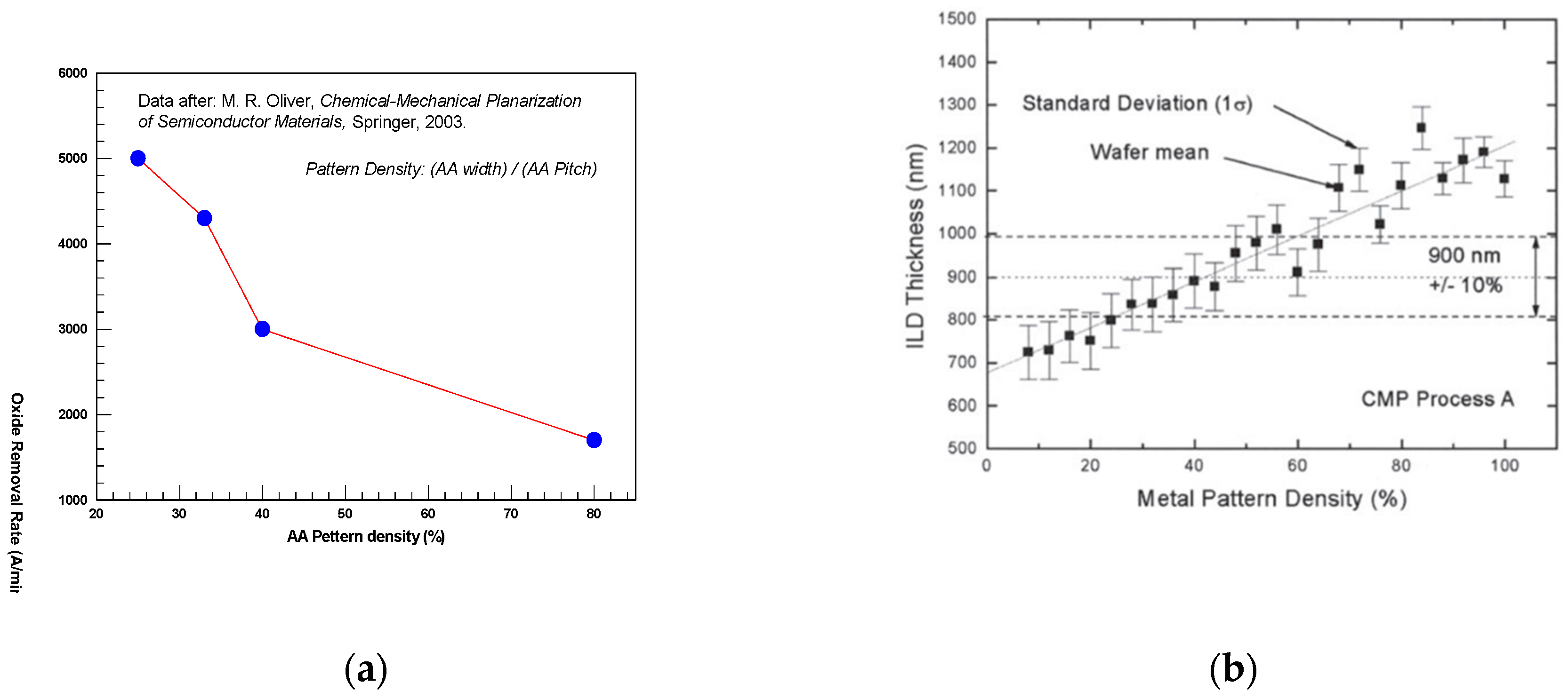
Figure 3a shows how the polish rate decreases with increased AA density [
5]. The reason for this is that for a given applied force on a smaller area, there will be an increase in the pressure, which will lead to higher removal rate. When features are eliminated, the polish rate then reduces to the rate of a planar surface. The time to reach this transition to planarity decreases with decreasing density. This is because the local polish rate increases with decreasing AA pattern density.
The process of ILD planarization in Al BEOL involves oxide CMP of the dielectric that takes place after metal sputtering and metal etch. A high metal (Al) pattern density means that more oxide needs to be planarized. For a given polish time, high density areas will have a higher dielectric thickness post CMP above the metal lines. The ILD thickness is measured on top of the Al features, and in this example (
Figure 3b) has a target of 900 ± 100 nm.
2.2. Dishing and Erosion
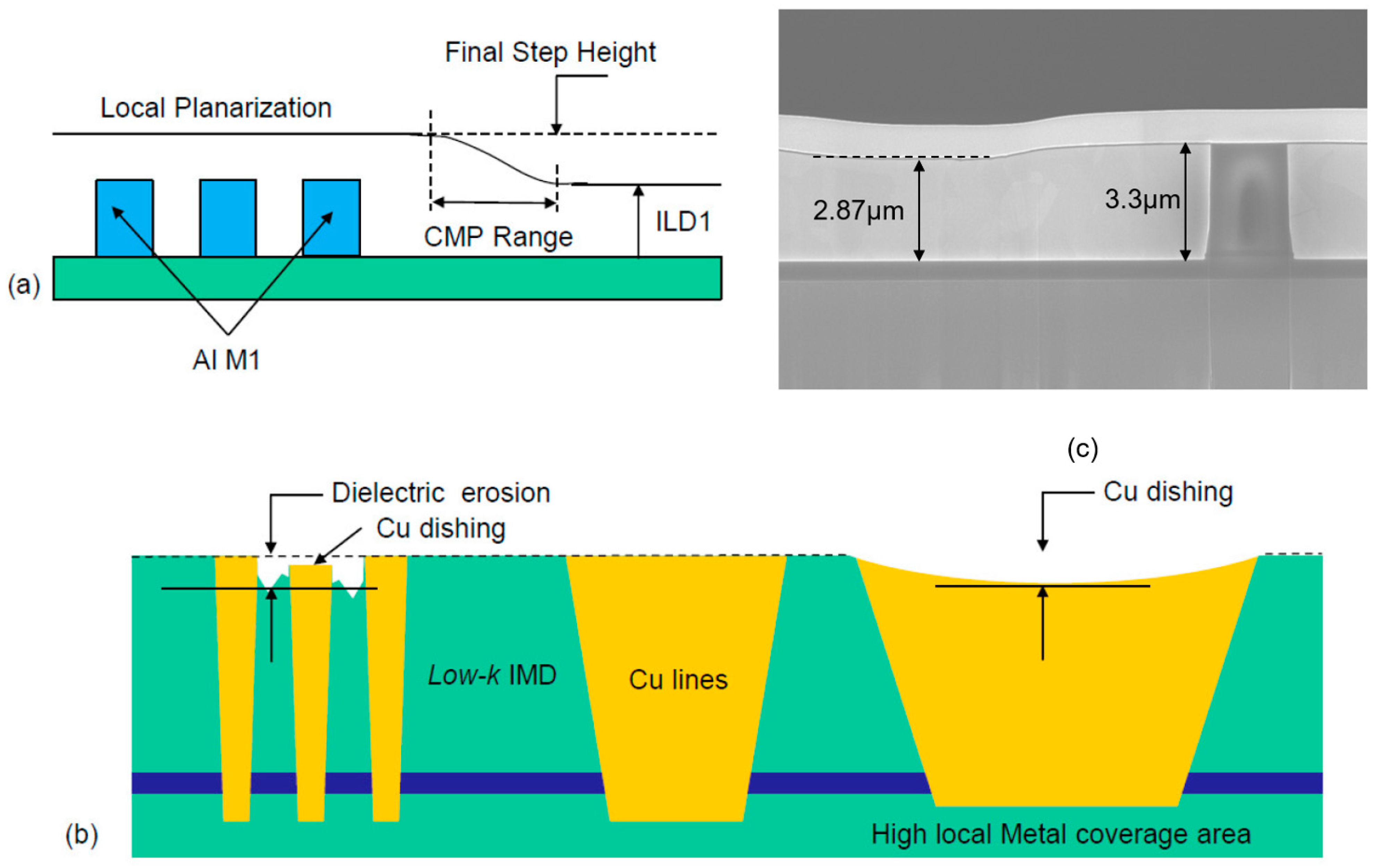
In a case were local uniform coverage is available on the wafer, local planarization can be achieved (see
Figure 3b for dielectric CMP over Al lines). However, a large coverage difference between two nearby locations will create a dielectric step with a range that depends on the coverage differences, the amount of polished film that has been removed, and the planarized material. The ILD over low coverage Al pattern will be removed faster compared to the ILD over a high coverage area.
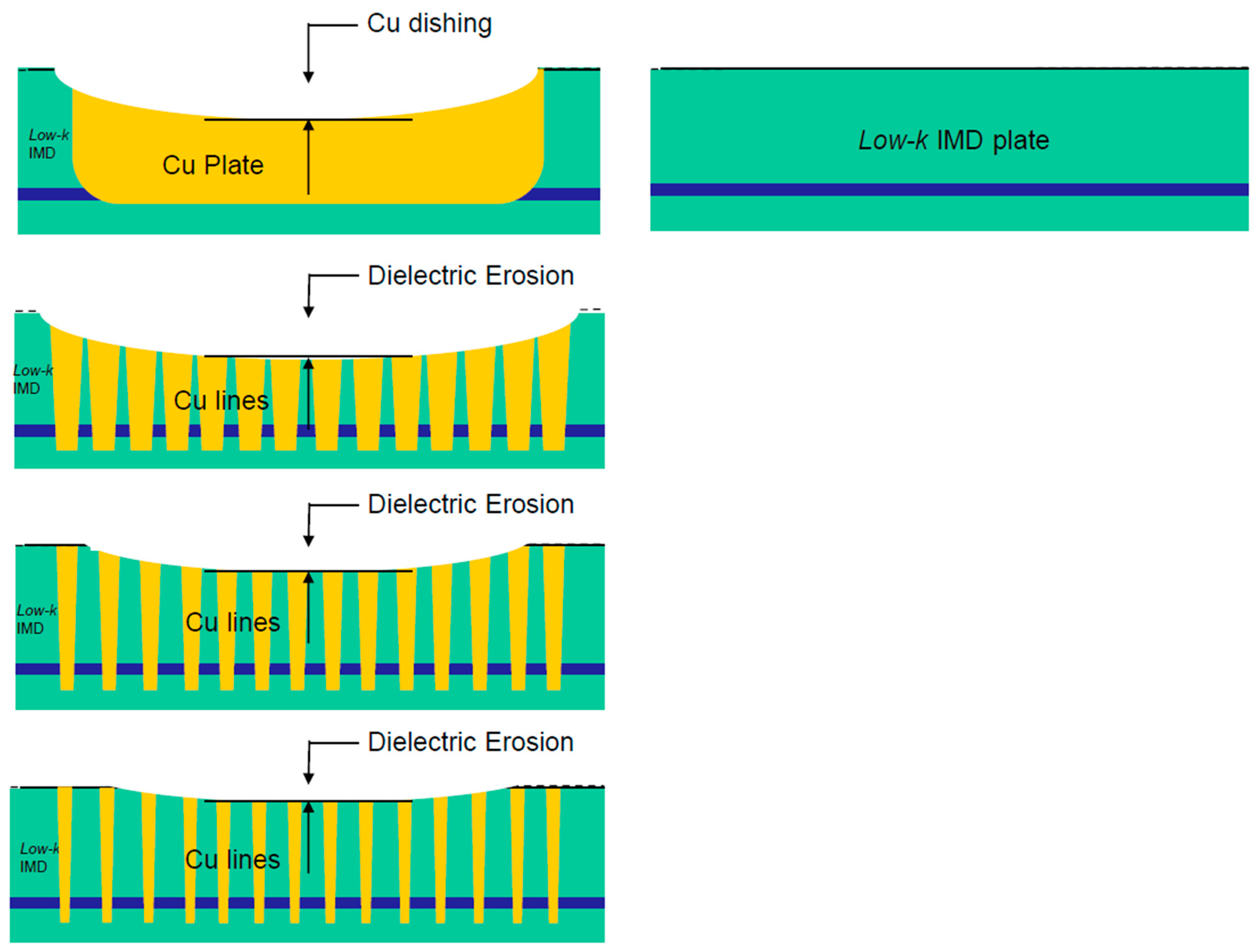
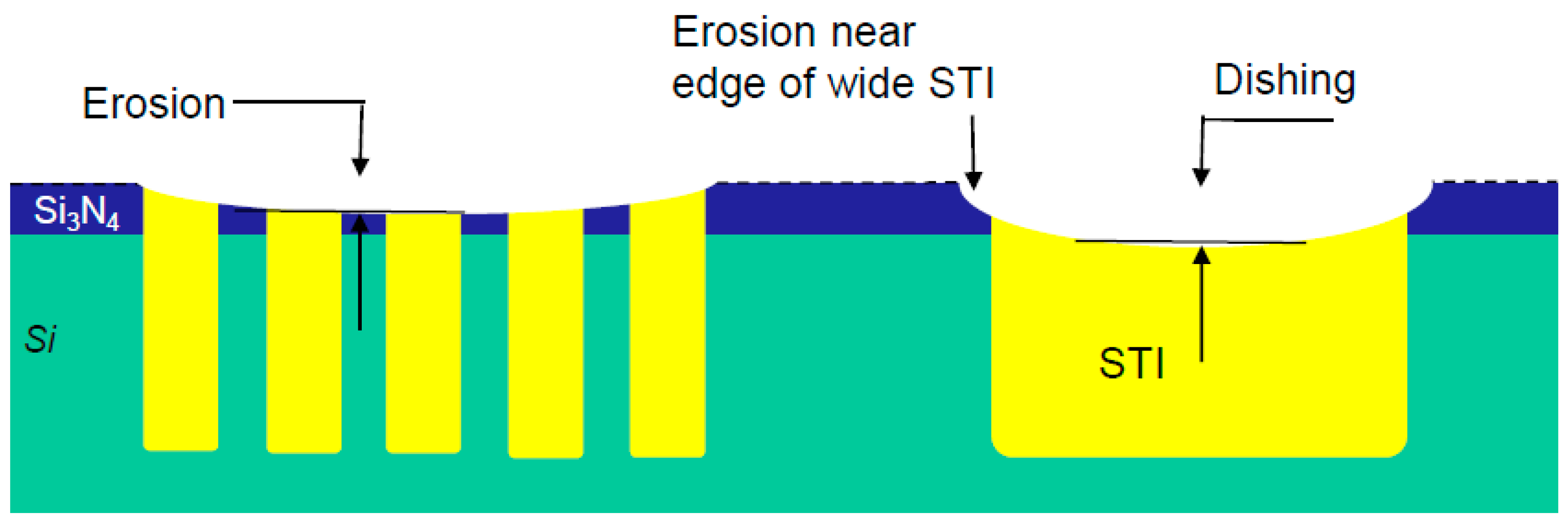
Dishing is the thickness loss at the Cu line in comparison to the oxide nearby. For STI, it is the thickness loss compared to the Si or SiN surface. Erosion is the amount of oxide lost between Cu lines in comparison to a field oxide far from the lines. Dishing and erosion (
Figure 4b) occur in damascene processes during the clearing and overpolishing stages. Dishing occurs due to differences in the polishing rates of the two exposed materials. For copper technology, the low-k ILD removal rate is much lower than the Cu removal rate.
Figure 4c shows an example of severe copper dishing for a 3.3 µm thickness (15 µm wide) copper inductor. The erosion is a result of polishing dissimilar materials that vary in pattern density. Oxide loss is more dependent on the pattern layout and takes place in cases of high metal coverage and with narrow dielectric spaces. The polish will reduce and potentially damage the narrow dielectric fins and yield dielectric erosion with metal loss.
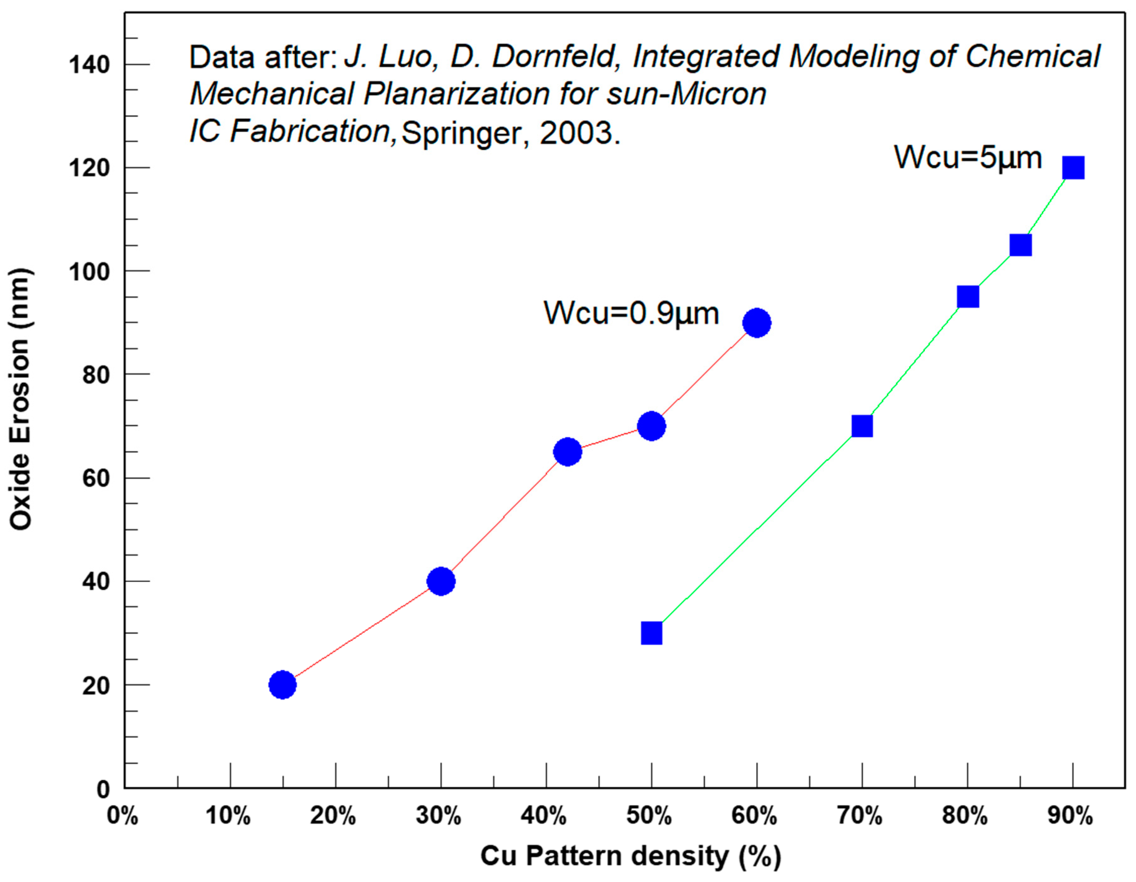
An example of the erosion dependency on Cu pattern density and Cu line/space widths is presented in
Figure 5, in which, for the same metal density, the oxide erosion decreases with increased line width. There are two reasons for the rapid increase in erosion with pattern density: a longer overpolishing time and higher pressure since there is less oxide area to polish [
7].
Dishing and erosion are controlled by the local pressure on features [
8]. The process parameters are downward force, slurry removal rate, selectivity of the slurry to barriers and dielectric, and pad condition. Polishing pads are quite flexible and have a surface roughness in the same scale as the metal line dimensions (pad asperity heights are typically 1–3 µm) [
5]. The slurry particle of fumed silica has a mean aggregate size in the range of 100–300 nm.
Figure 6 illustrates erosion dependency on the coverage and line width (higher coverage results in more erosion).
The result of dishing and erosion, in addition to the general CMP non-uniformity, is Cu thickness variations [
7]. The maximal line thickness variation at a typical foundry process is ±15%. Higher variations yield non-optimized photo depth of focus (DOF), high BEOL resistance capacitance (RC) variation, and topography that can lead to Cu residues in the upper layers.
During Cu CMP, recessing can also take place. A recess (
Figure 7) is characterized by a small sharp vertical step at the edge of metal features, unlike dishing and erosion, which are characterized by gradual changes in vertical dimensions and a relatively smooth topography. Recesses can be understood as a degradation of the final planarity arising from the complete removal of the metal overburden. However, unlike dishing, recessing affects features regardless of size. The exact source of recessing is not entirely clear in every case. However, it can generally be attributed to chemical attack or corrosion of the metal surface, either during over-polishing or during post-polish cleaning.
In processes with low copper coverage, like Via CMP for single Damascene integration, a severe recess may yield an open via (
Figure 8). To eliminate that, the process should be optimized and split into several steps. Isolated vias tend to suffer more than arrays of vias. Therefore, design rules for via coverage were introduced into the foundry design rule manual (DRM). Short over-polish times should be used for lonely vias. Finally, the slurry chemistry has a very large impact, i.e., insufficient corrosion inhibitor will lead to large recesses.
Thick and wide Cu lines are sensitive to recessing, especially when a long polish time is required to clear the Cu overburden.
Figure 9 shows such a case, in which a metal line recess created topography which caused poor patterning of the following via photo resist. This led to an “undefined via.” Process improvements solved this problem.
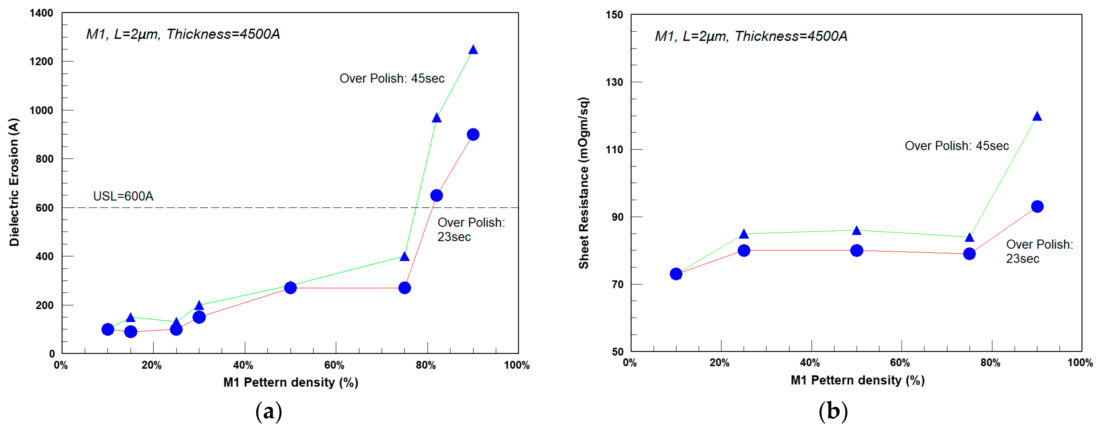
Figure 10 shows our experimental data regarding the dependency of erosion on local Cu density. Using a set of test chips with different coverages (all with L = 2 µm), the dielectric erosion was measured. Using an upper limit of 600 A, the maximal coverage can be extracted as around 80%. Naturally, longer over-polish times yield larger erosion. M1 sheet resistance (
Figure 10b) showed the same dependency to coverage as erosion. Setting an upper limit of 100 mOhm/sq yields a maximal coverage of around 80%. The structures with coverage >80% also showed high Sheet Resistance (Rs) distribution.
2.3. Oxide CMP Process
In oxide CMP, the water diffuses into the oxide network and causes the rupturing of Si–O bonds [
9]. Oxide surface weakening occurs by the following equation:
Once all the Si–O bonds for a given Si atom are hydrated, Si(OH)
4 is formed, which is highly soluble in water at high pH levels. These reactions are accelerated by the compressive stress imposed on the surface by abrasive particles [
9]. The hydrated Si surface is much softer than the initial SiO
2 net and is therefore much more easily removed by abrasive particles. The most basic material removal model is described by Preston’s equation, which was initially introduced for glass polishing:
where
RR is the material removal rate of the polished material,
Ke is a calibration coefficient,
P is the downward pressure, and
V is the relative velocity between the wafer and pad. The equation demonstrates the linear dependency of the material removal rate on the pressure and velocity [
7]. The equation does not represent all dependencies (e.g., on slurry and pad properties), and in many cases, it does not perfectly correlate with experimental data. Brown and Cook [
6] developed a physical model that takes consumable and wafer parameters into account:
where
E is the Young’s modulus of the wafer materials. This model proposes an interaction between the abrasive particles and the wafer surface that is proportional to the particle penetration of the oxide.
Some researchers assume that a fluid film exists between the wafer and pad interface. Runnel [
10] developed an erosion-based model in which erosion/material removal rates at each single point are given through fluid stress tensors:
where
is a calibration coefficient,
is the sheer stress due to the slurry flow and
is the normal stress.
When pattern wafers are polished, the wafer pattern density, feature size, and pitch has a large impact on the RR at different die locations. A model was developed at MIT by Stine et al. [
11] and the experimental data indicated that the pattern density
ρ(
x,
y), defined as the ratio of the raised area to the total area as measured in a window of a given size, has the strongest impact on the within-die non-uniformity (WIDNU). This is explained by the relationship between pattern density and pressure. In the high-density area, where the oxide area contacted by the pad is larger, the effective pressure P/
ρ(
x,
y) is lower and the material removal is reduced. Equations for the material removal rate based on Preston’s equation were developed by Stine et al. [
12]:
where
Z is the height of the oxide pattern feature to the substrate,
Zl is the as-deposited step height,
ρ(
x,
y) is the effective pattern density,
MRRi =
KePV is the blanket wafer polishing rate (based on Preston’s equation), and t is the polishing time. For time
, there is still a step height, and once
, the
RR is of a blanket wafer. Using this model enables researchers to consider the impact of pattern density.
2.4. STI CMP Process
At STI CMP, the process needs to planarize the dielectric that fills the trenches with good uniformity and minimal process defects. The main challenges of STI CMP are as follows:
Clearing all of the oxide above the SiN: The STI CMP needs to remove all of the oxide above the SiN, which serves as a “stopping” layer. Large areas with high coverage are close to a blanket wafer. The result is a very low RR, and there is a high risk of leaving oxide residues. This problem depends on the STI fill process, since different deposition processes will result in different overfills.
Soft stop on the SiN: Polish should not damage the Si surface. Scratches or lattice defects lead to a degradation of reliability. To address this concern, it is common to use Ceria (CeO
2) as the abrasive particle instead of silica. Ceria has a high RR and higher selectivity between oxide to SiN. In addition, the SiN needs to be thick enough to prevent scratches that occur during the CMP process from reaching the Si surface. The CMP process is faster at corners and along edges of topography. Therefore, the SiN at the edge of the AA region near the STI will be polished faster than areas far from the STI (
Figure 11). This problem is more severe for large AA spaces (wide STI).
STI Dishing: Since the SiN has a lower RR than the oxide, dishing in the STI occurs. In severe cases, poly located over STI will be poorly defined due to limited DOF.
2.5. W and Cu CMP
Kaufman et al. proposed a model for tungsten CMP after the contact fill, which was widely accepted [
13]. According to this model, a passivation layer of tungsten oxide is created by the slurry chemicals and the aqua solution. This layer is softer than the bulk of the W; therefore, it is more easily removed by the slurry abrasives and polishing pad mechanical abrasion. A fresh tungsten surface is exposed, passivated, and removed, and so on. The passivation layer also prevents dissolution of the tungsten film in the low areas in cases when the slurry chemistry has a high static etch rate [
9]. Hydrogen peroxide is used in all metal CMP slurries as an oxidizer [
7].
The removal of Cu consists of several steps [
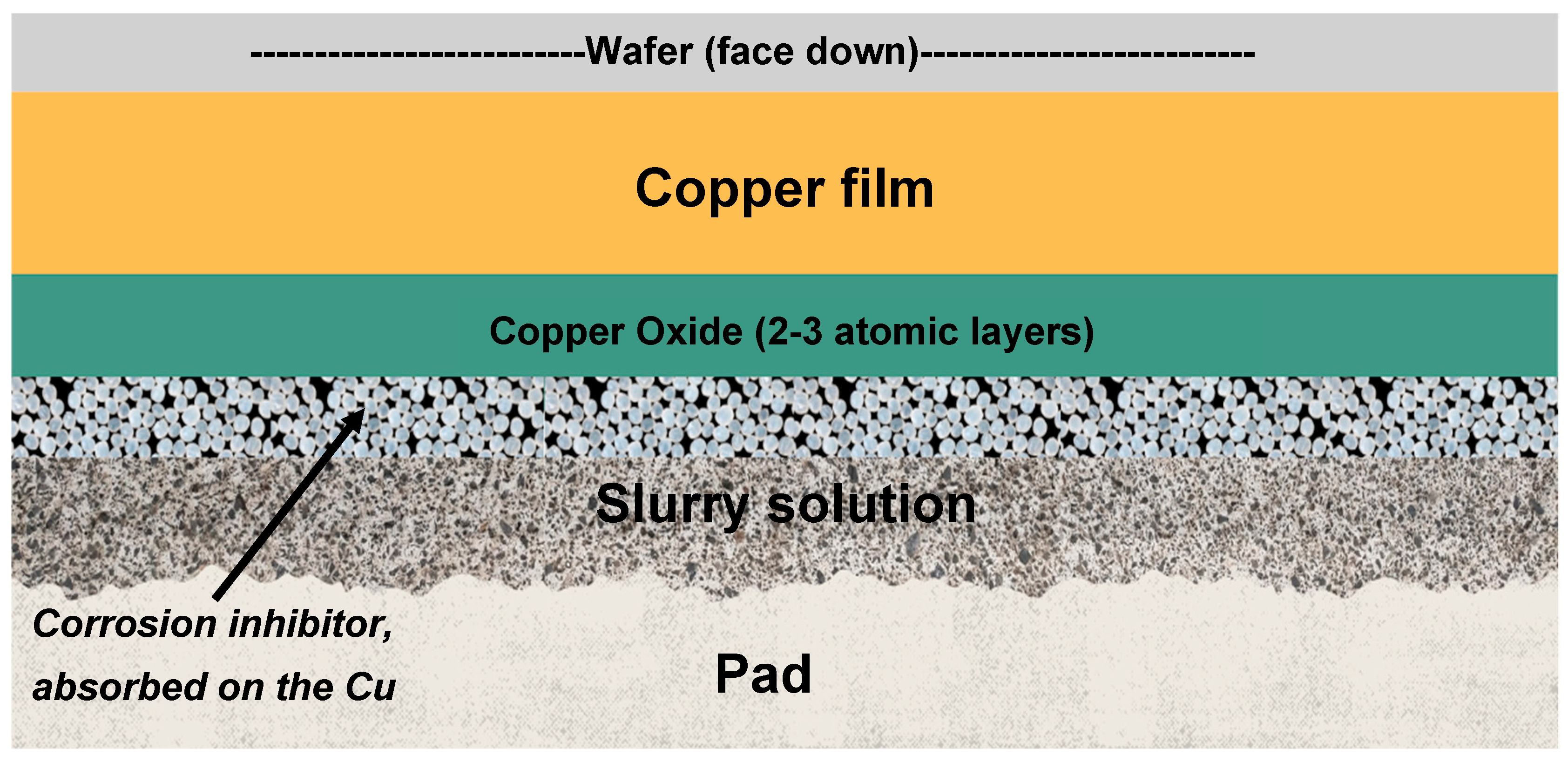
8]: (1) dissolution of Cu to form thin atomic layers of oxides of Cu, (2) mechanical removal of the material using slurry particle abrasives, and (3) sweeping away the abraded material suspended in the solution by slurry flow. An example of the slurry components and the interactions with the Cu surface during polishing can be seen in
Figure 12.
The hardness of copper (1–3 GPa) falls between that of tungsten and aluminum. Thus, Cu is easier to abrade than W. The hardness of Cu is significantly lower than the slurry abrasive particles, which are usually silica. Thus, chemical action on Cu to form a harder oxide is essential before the mechanical abrasion of Cu to prevent the formation of defects during the CMP process [
9].
The layer formation on the surface can be explained by electrochemical reactions such as
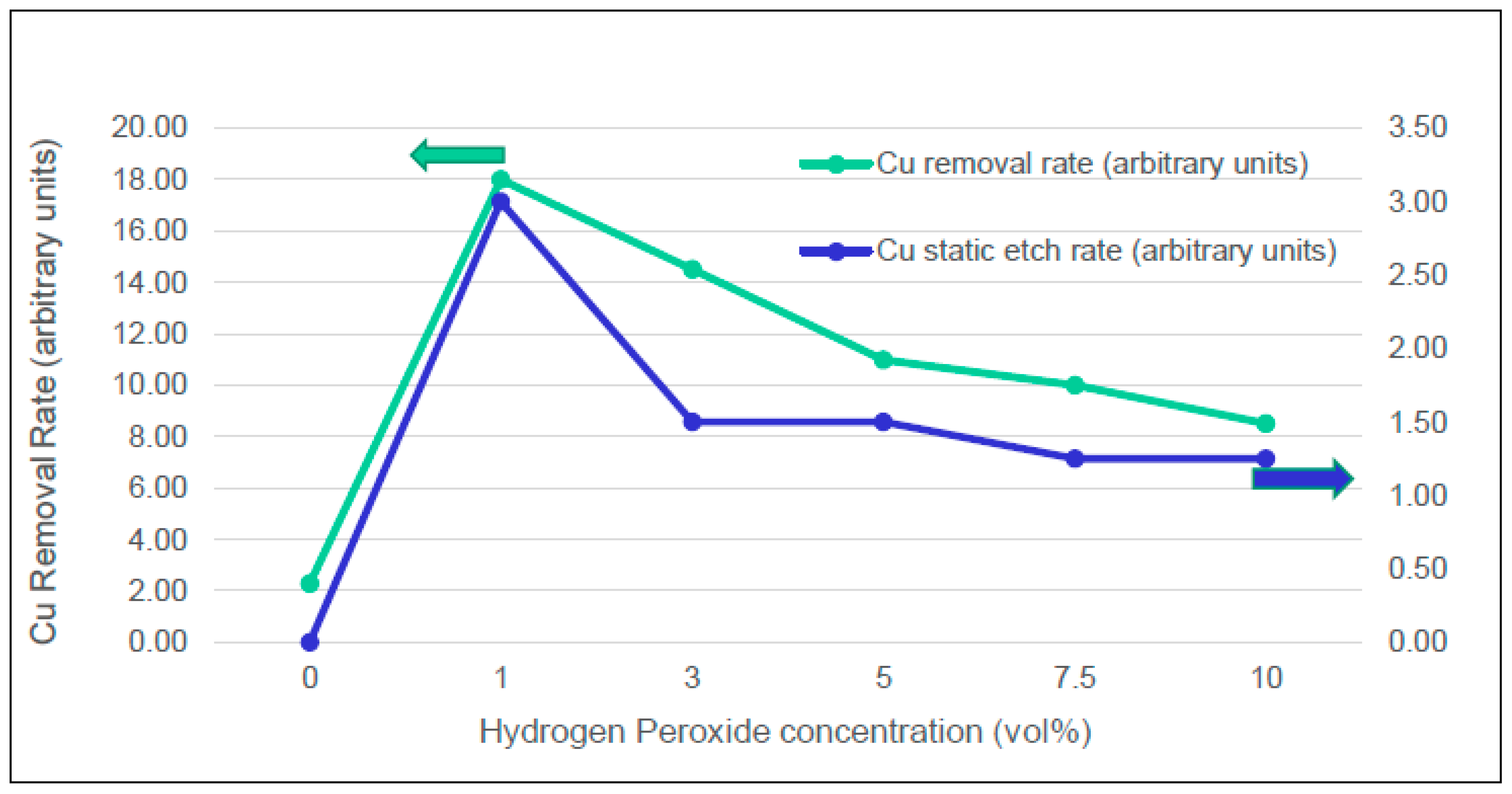
Oxidizer: For metal CMP, an oxidizing chemical environment is required. During copper oxidation, neutral metal atoms lose electrons and take on a net positive charge. The metal atom loses the valence electrons to atmospheric oxygen to form metal oxide. The oxidizer species contained in the slurry undergo reduction when the metal surface is oxidized. Both the static etch rate and dynamic removal rate of Cu depend on the H
2O
2 oxidizer concentration in the acidic medium (
Figure 13). The removal rate increases with increase in H
2O
2 concentration up to a certain point [
8]. The decrease in removal rate is attributed to an increase in surface passivation. A typical slurry used in the field includes about 1% hydrogen peroxide concentration.
Buffering: Cu slurry is typically held close to neutral pH to control the removal chemistry. For pH > 7, a buffer system based on a solution of a weak base and a corresponding salt (e.g., ammonium hydroxide and ammonium chloride) is used.
Corrosion inhibitors: Added to the slurry to suppress Cu corrosion and dissolution. The inhibitors are adsorbed onto the metal surface to form a protective coating, which causes the inhibition of oxidation of the metal surface to some degree. Corrosion inhibitors are crucial to prevent dishing and post-CMP corrosion of Cu lines.
Surfactants: A surfactant is a dissolved chemical agent that reduces the surface or interfacial tension of a liquid phase, typically water, in contact with some second phase. The surface tension of aqueous media containing surfactants is significantly lowered, which results in better wetting. That is, surfactants change the interaction between abrasive particles and the solution. This provides better particle suspension and a collateral reduction in particle agglomeration. It is particularly important for copper CMP, since copper is soft and easily scratched.
Complexing agents: Metals containing complexes can be formed in aqueous media. A metal complex is a chemical species that has a metal atom in a central position, to which various atoms or molecules are chemically bonded. In general, complexation results in dissolved metallic species that are thermodynamically more stable than simple aquo ions. For metal CMP, complexation can be generally expected to increase the removal rate; therefore, complexing agents are sometimes added intentionally to the slurry [
5].
2.6. Cu CMP Modeling
CMP nonuniformity can be classified as short-range, long-range or wafer scale [
14]. The model described below is for long range. The fact that the slurry is a multi-component makes the theoretical modeling of Cu CMP more complicated. The model should take into consideration the different pattern densities and feature sizes, the removal rate selectivity between Cu and the liner (usually Ta/TaN), and the removal of the dielectric antireflective coating (DARC), which requires an additional CMP step.
Most of the models for copper CMP are based on Preston’s equation. Tugbawa et al. [
15] modeled the pattern dependency of the Cu CMP by dividing the process into three stages: (1) Bulk Cu removal, (2) barrier removal (where dishing evolves), and (3) the overpolish step (where erosion evolves). Using removal rate data from blanket wafers, the model establishes an empirical relationship between the material removal rate and polish pressure. This data is then used to calculate the polish pressure and removal rates as a result of the step height and pattern density. For each of the above three steps, a set of equations represent the removal rate of the high-density areas and the low-density areas. Tugbawa et al. used MIT-SEMATECH test masks, which came to be the common industry vehicle for modeling a copper CMP process. The mask has a variety of structures with different densities and pitches to retrieve the empirical data of dishing and erosion. Finally, the experimental data is used to calibrate the CMP model for the exact consumable set.
The change in step height along with polish time is described by
where
where
is the blanket Cu removal rate,
is the pattern density, and
is the step height from which the down pressure area removal rate starts to be significant. The
data is obtained from the test masks.
2.7. Cu Electroplating
The Cu electroplating process is also dependent on the feature size and density. The process filling is “bottom-up,” which helps to prevent void formation in high aspect features. This is achieved by additive chemicals known as accelerators, suppressors, and levelers, which are added to the plating solution [
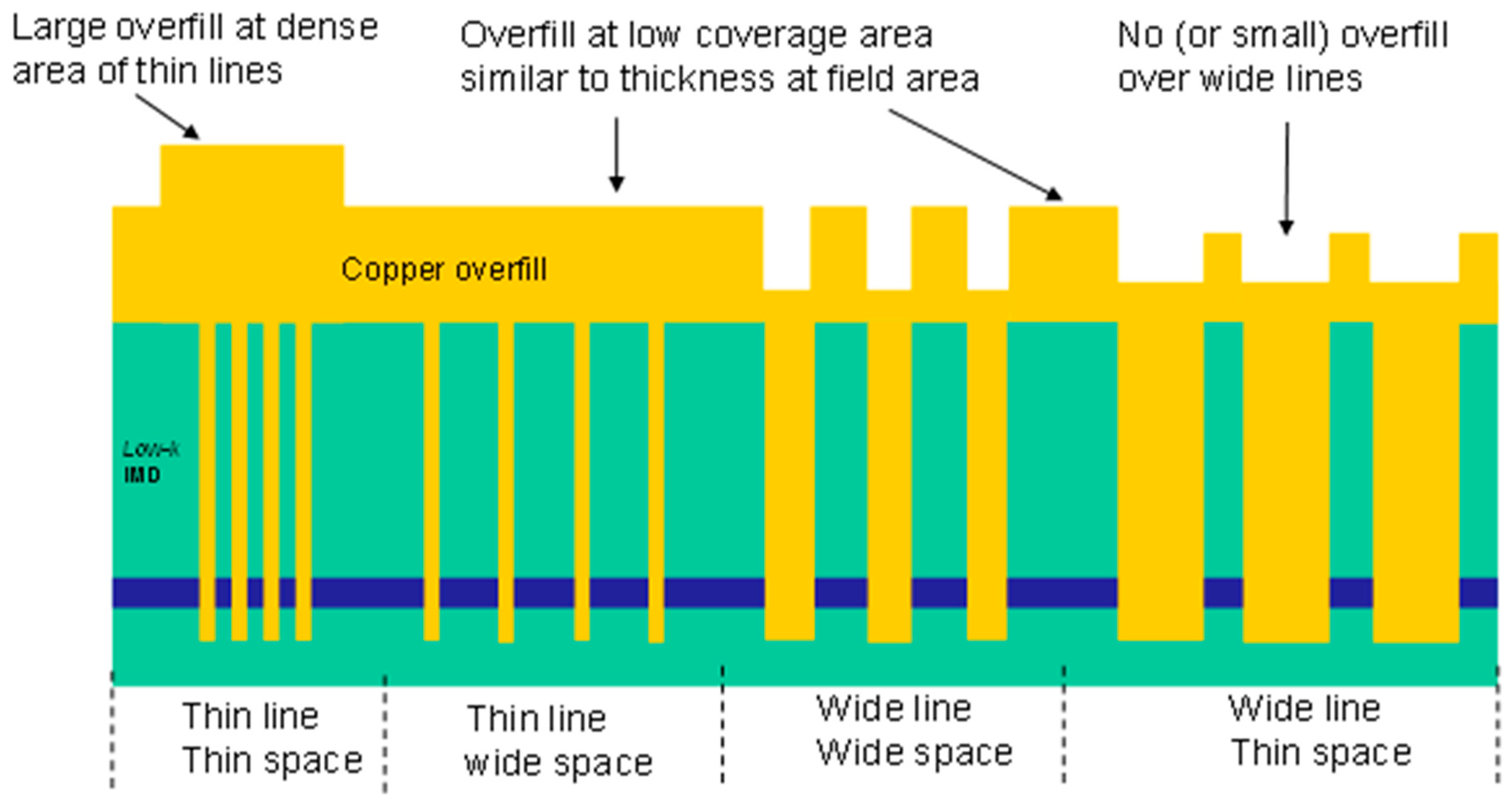
5]. However, it leads to substantial thickness variations of the copper overburden (“overfill”). In particular, copper is relatively thick over dense arrays of minimum dimension features and is thinner over wider features.
Figure 14 presents a schematic example of the Cu thickness post-electroplating deposition (ECD) of different Cu line widths and densities.
Longer polish times are needed to remove the thicker copper deposition over small dense features. However, this would cause over-polishing for wide features. In addition, it can result in severe dishing, erosion, and field loss [
5].
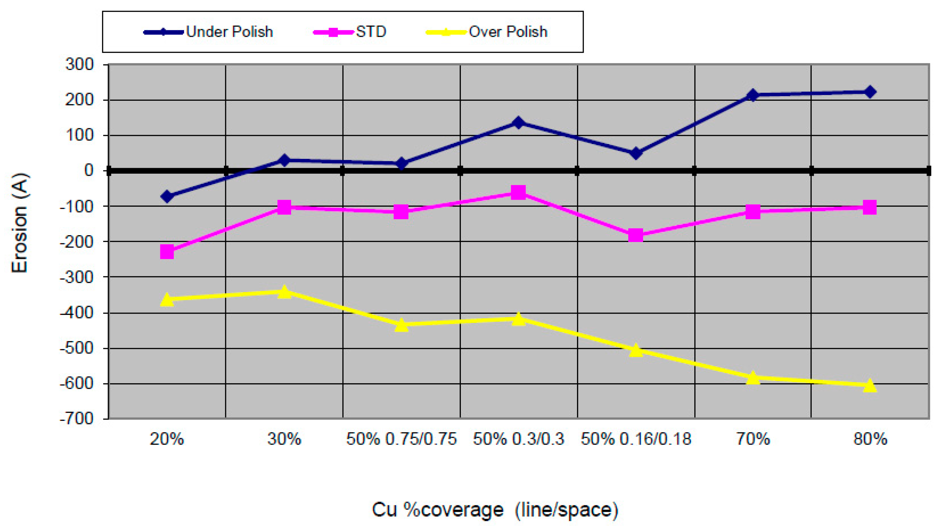
Figure 15 shows our results for the erosion dependency on coverage under three different process conditions. For over-polish conditions, higher density increases the erosion. In addition, at a similar density (e.g., 50%), wider dielectric spaces result in less erosion. A positive erosion value (usually referred to as “negative erosion”) means that the dielectric thickness of the measured structure is higher than the field oxide reference level. This is explained by the plating process, which has a higher Cu plating thickness (overburden). When polished, the low coverage areas are cleared from copper before the high coverage areas, so the dielectric is exposed sooner, resulting in higher levels of erosion.
Another aspect that needs special attention is post-CMP cleaning. The low-k materials are more hydrophobic than SiO2, which results in less effective cleaning and can leave water marks. Wafer drying using isopropyl alcohol (IPA) is more effective than spin drying at removing all of the water from the dielectric surface and eliminating the water drying marks.
3. Global and Local Planarization—CMP Range
Global planarization depends on coverage difference of neighboring areas. Therefore Dummy fill insertion is used to achieve as uniform coverage as possible. This is done with dummy AA (DAA), dummy poly (DGC), and dummy metal (DM). The distance of the inserted tiles to neighboring features has an impact on the polish rate at the location of interest (see
Figure 4a). The planarization length also depends on the CMP process parameters such as head pressure, pad condition, polish time, etc. For Cu technology that includes a Ta/TaN barrier, the CMP involves the removal of different materials that also affect the CMP range [
16].
Typical values for oxide CMP have been estimated as 0.5–2 mm [
17] and 3–5 mm [
18]. A typical value used by the industry is about 500 µm. For Cu CMP, the interaction length was estimated as 100–200 µm [
17] and 50–100 µm [
16]. The typical range used in the industry is 25–100 µm, varying depending on the metal thickness—the thicker the line is, the larger the interaction length. Lakshminarayanan et al. [
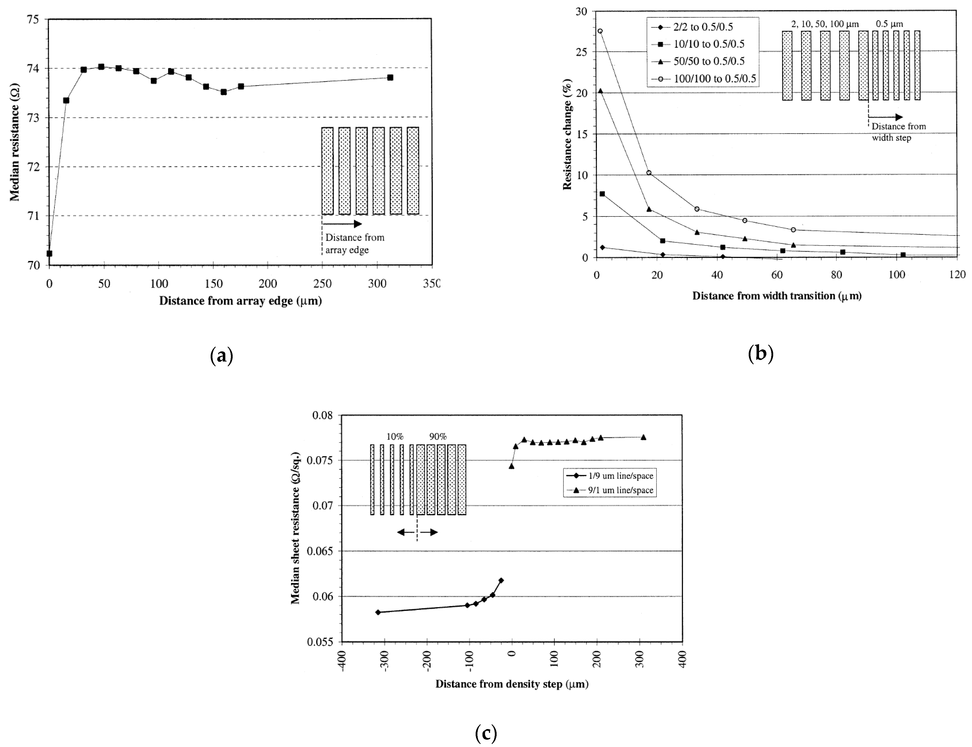
16] studied the effective pattern interaction distance using a set of structures with different coverages and measured the line resistance.
Figure 16a shows the median resistance of a structure with L/S = 3/1 µm and 75% coverage as a function of the position on the array. The resistance at the array edge increases rapidly, proceeding inwards (due to dielectric erosion), and stabilized about 30 µm from the edge. We can conclude that the range is about 30 µm and resistance is stable beyond that range.
Figure 16b shows the spatial change in median resistance of 0.5 µm lines from step pitch structures. These structures contain two adjacent arrays at a constant coverage of 50% (L = S) but differing line width. The array on the right contains 0.5 µm lines and an abrupt change occurs when the line width on the left array switches to 2, 10, 50, or 100 µm. The impact of altering the line width at a fixed global density was analyzed by measuring the resistance of the 0.5 µm lines as a function of the distance from the last wide line. We can conclude from the chart that the higher the difference in the line width outside the array from the line inside the array, the higher the resistance and the interaction length for the lines inside the array. For line width < 10 µm, the resistance was stabilized after 20 µm. However, for a line width of 50 µm, the interaction length increased to around 60 µm.
Figure 16c also shows the effect of abrupt coverage change for a step in pattern coverage from 10% (L/S = 1/9 µm) to 90% (L/S = 9/1 µm).
Figure 16b shows that if the line width ≤ 15 µm and the maximum coverage difference between arrays is <30–45%, the resistance variation will be <10% and controllable. This type of information, translated into a set of DRs, is presented later.
4. AA, Poly, and Al Global Coverage Rules
Density rules were introduced into the DRM by the manufacturers to manage variation in the line height caused by the CMP process, as well as differences in the line width caused by RIE processes. The primary solution to minimize this variation is to add a nonfunctional and electrically meaningless AA, poly, and metal polygons in order to try and achieve an even global coverage of AA or metal across the die.
For DRC (DR checking) purposes, the global coverage is mostly calculated (e.g., for poly) as
The RIE process used for patterning is sensitive to the density over the wafer. In this case, the etch process was designed to maximize the etch rate, and regions with a large open area (clear on mask or low coverage) will be faced with local low plasma densities and low etch rates. The simple process explanation for Al etch is that the lower the pattern density, the higher the amount of Al to be etched. For Cl-based RIE, it means higher consumption of Al atoms during etching, which decreases the Cl atom density and etch rate.
Insertion of dummy patterns is one of the ways to reduce the macro-loading that takes place due to overall depletion of the reactants with more exposed etch areas. The level of macro-loading also depends on the process chamber design and the process parameters, mostly the gases and the power. Naturally, thicker layers (e.g., >1.5 µm Al layer) require longer processing times and therefore suffer from larger variations. During Al RIE, polymer generation protects the sidewalls. However, excessive polymers due to the long process time may cause the profile to become sloped.
The micro-loading effect means that dense lines will have lower etch rates than isolated lines. A “ground-rule” for data leading to dark layers (e.g., poly or Al, where the drawn data mean chrome on the mask and positive photoresist on the wafer) is that isolated lines will have higher etch rates, so there are lower critical dimensions (CDs) vs. dense lines. This also leads to iso-dense CD bias.
In many cases of Al etch, polymers generated during the RIE process protect the sidewalls and yield larger CDs for isolated lines. A team from X-FAB [
19] studied the impact of different global densities on the 3 µm Al profile and line width dimensions. A 3 µm Al line is also typical in Cu technologies and is located below the passivation. The layer is used for bonding purposes as well as for connecting different bonding pads as RDL. Global coverage lower than RDL.C.1 (see
Table 1) may induce fewer polymers due to there being less photoresist available, which leads to sidewall attacks and potential bottom notching. Low coverage also causes large CD bias. Coverage higher than RDL.C.2 yields low etch rate and risks an incomplete etch with potential short and high CD bias. A way to set the global coverage limits is to measure the dependency of the sheet resistance—for the same coverage, wider lines will have lower sheet resistance due to their larger grains. The higher the coverage or larger the line CDs and lower the sheet resistance. To satisfy upper specified limit for all line widths, the minimal coverage should be set to 10–15%. For a poly etch, typical numbers for GC.C.1 and GC.C.2 are about 10% and 45%, respectively.
5. AA and Copper Local Coverage Rules
Local coverage rules (
Table 2) were introduced by manufacturers to support the CMP process. For DRC purposes, the checking window is stepped in most cases, by half-size of the window size. e.g., a window of 200 µm × 200 µm will step by 100 µm, that is, each location on the wafer is included in four different checks.
The coverage range between maximal and minimal density is reduced as technology advances. For copper technology, a typical minimal coverage is 10–15%. The typical maximum coverage is 80%, but this is reduced for advanced technologies to about 73% or even <70%. In many cases, instead of or in addition to the maximum coverage reduction, the window size is also reduced. Typical windows of 200 µm × 200 µm with a step of 100 µm have been reduced to 100 µm × 100 µm with a step of 50 µm or even lower. For example, coverage ranged from 35% to 70% in a window of 10 µm × 10 µm [
21]. In addition, the gradient requirement (see rule M.C.34) was introduced, seeking a maximal value of 30–50%.
6. Minimum and Maximum Copper Coverage Design Rule Setting
Setting both minimal and maximal coverage rules can be based on line resistance measurements combined with SEM analysis. The sheet resistance is inversely proportional to the line thickness (t); thus, a line located at a high coverage area will face dishing and higher resistance, similar to the pattern interaction distance study described earlier [
16].
The line resistance depends on surface and interface scattering, which becomes dominant as the relative thickness of the diffusion barrier increases with technology scaling and due to the reduction in the film thickness that becomes comparable to the mean free path (which is ≈40 nm at room-temperature). In addition, the line width and film thickness reduction lead to smaller grain sizes and a short distance between scattering barriers. The result is more scattering from the sidewalls and from the grain boundaries. More details on the line width resistivity dependency are given in [
22,
23]. Therefore, setting the coverage rules needs to take into consideration the line width. For this purpose, dedicated test chips were developed, i.e., the MIT vehicle [
24] described earlier that was also used by IDMs [
16] and foundries [
18]. This test chip contains several modules, where each module is larger than the copper CMP range.
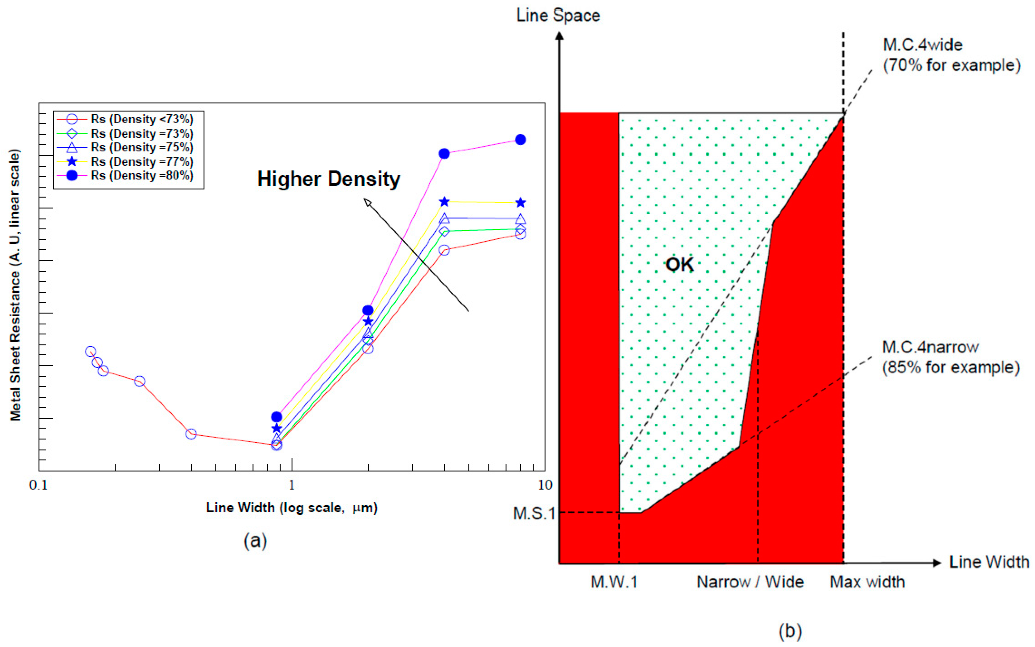
Using the test chip, we found the dependency of sheet resistance on line width at different densities (
Figure 17a). For narrow lines (<1–3 µm), the scattering effect is seen clearly with a negligible coverage dependency. For wide lines (>5–10 µm), the dishing effect yields higher sheet resistance, with a clear coverage dependency—the higher the coverage for the same line width, the stronger the dishing. Using the maximum/minimum sheet resistance limits, as defined for the technology, and taking into consideration the process variability, rules M.C.3 and M.C.4 can be extracted without any dependency on line width. Afterwards, the maximal line width that can be used with the technology (without metal slits) can be extracted, using the upper limit of the sheet resistance and the upper density limit. Analysis should also take into consideration that thicker metal lines have larger grain sizes that slightly reduce the sheet resistance. In
Figure 17, line width where dishing begins is easily observable.
Sheet resistance charts, like the one shown in
Figure 17a, are used to enhance the accuracy of RC extraction of interconnects. For each segment of a metal line, the number of squares (width/segment length) is calculated. Then, a local window is defined around the segment and the local coverage is extracted. This local coverage, together with the line width, is used to define the local effective sheet resistance. Finally, the segment resistance is calculated by multiplying the number of squares with the local effective sheet resistance. The team from LG Electronics developed a very similar process that consists of CMP modeling for accurate RC extraction [
25].
Analysis of
Figure 17 shows that an array consisting of narrow lines only has a higher coverage limit than an array with wide lines only. The definition of a “wide” line can also be extracted from
Figure 17a, and it depends on process parameters like the metal thickness, slurry type, the amount of CMP overpolish, and the R range. A typical value for a wide line can be >4–8 µm. Lines with a width below the figure taken for a wide line are referred to as “narrow.” In
Figure 17b, we describe the minimal and maximal line width and space, based on the coverage limitations. For narrow lines, a fine space can be used, delimited by M.C.4narrow. Using wide lines demands larger spaces limited by M.C.4wide. The line/space domain is limited by the minimal and maximal line width as well as the minimal line space. This coverage dependency on line width is integrated into the coverage rules.
With these dependencies, we can set a simplified design guideline—it is better to replace a single wide line with several narrow lines. This costs more design area but allows a higher maximum local coverage to be used.
7. Dummy AA (DAA), Dummy Poly (DGC), and Dummy Metal (DM) Rules
The dummy rules were set by the integration team for two main reasons: first, to be able to conduct quality assurance (QA) on the dummy insertion utility in order to ensure that a proper fill was done; and second, to guide the designer in case manual dummy insertion is required at local spots that faced with poor insertion efficiency.
Table 3 lists some of these rules.
Setting rule DAA.D.1 needs to consider stress induced into the MOSFET by the STI due to the length of oxide diffusion (LOD) and oxide space effects (OSE). Researchers from AMD [
27] showed an example using the DAA to improve 65 nm standard cell library performance. From this example, we can list the following guidelines:
Guideline 1: Insertion of DAA next to NMOSFET regions should be in the lateral direction only. Then, the STIW (STI width) parallel to the poly gate will be reduced, resulting in higher electron mobility.
Guideline 2: For the PMOSFET, regions near the P+ AA region should be left blank in the lateral direction and DAA insertion should occur in the orthogonal direction only. By that, the STIL (STI length) orthogonal to the gate is reduced, resulting in higher hole mobility. Following these guidelines improves the overall circuit performance by 8% [
27].
If DAA is too close to the WN (N-Well) junction (rule DAA.D.2), it will degrade the WN/PW and the WN/Psub junction breakdown [
28]. The team from Tower found that without dummies, the intrinsic WNH/Psub (high-voltage WN)/Psub) junction breakdown (BV) was about 22 V. However, after DAA insertion, a soft leakage current was observed, which increased as the EXWELL (a native layer to block the P-Well implant) grew. The explanation for this is that the DAA located close to the WN edge (DAA.D.2 < 1 µm) introduced a leakage path from the Ntap, through the depletion region at the EXWELL into the silicide dummy and to the substrate. The larger the EXWELL, the larger the WNH depletion region and the higher the leakage.
The metal dummy’s width and space are set based on the desired coverage under the limitations of the insertion efficiency. Another limitation for having fine dummy features is the overall file size, which can increase significantly with finer dummy features.
For analog and RF circuits, both DM.D.1 and DM.D.2 are critical rules. The distance setting is a balance between insertion efficiency and coupling capacitance to active metal lines at the same layer or the wire below or above. A smaller distance means there are more dummies and a higher coupling capacitance, which slows down the IC. In most cases, the common practice is to set a very conservative distance (>1–5 µm), so that the coupling capacitance is negligible compared to the total capacitance of the line.
8. Multilevel Coverage Integration Effects
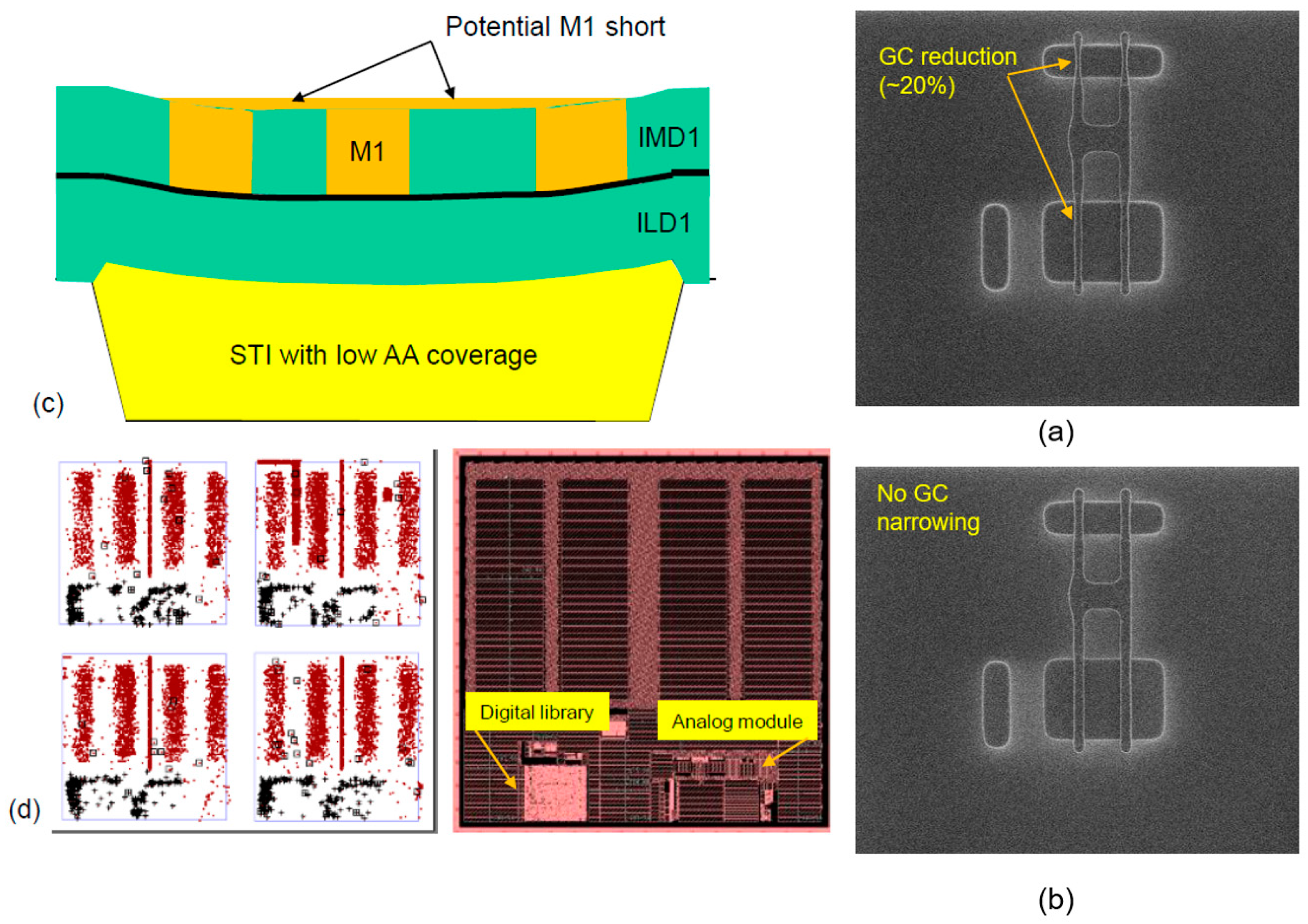
Low local AA coverage (<AA.C.3) may result in a non-uniform STI thickness in large STI areas. The resulting lack of uniformity of poly lines would lead to high variability of poly resistance. STI dishing has a negative impact on GC (poly) CDs, mainly in isolated small AA areas surrounded by wide STI areas (
Figure 18a). The dishing that occurred in this case was >750 A, and the bias between wide and narrow STI (at the same site location on the wafer) was >1500 A. The high dishing introduced a focus limitation during GC photo, and because of that, the GC CDs were very narrow (>20% compared to the regular case), yielding a high leakage of current. In many cases, an anti-reflecting coating (ARC) layer is placed above the poly. This layer is very sensitive to topography, so in the case of severe STI dishing, the ARC thickness over the AA will be thinner and yield narrow poly lines. The introduction of DAA together with CMP process optimization resolved the dishing problem and led to regular transistor behavior (
Figure 18b). Another potential problem is with the contact landing on poly located over a large STI area—the contact etch is not deep enough to reach the poly line. An example of another issue we faced was with a set of interdigitized M1 lines with a long parallel length of around 3 m, drawn with the minimal L/S allowed by the platform DRM. The structure was located over a large area of STI only (without dummy AA) and showed a low yield of 40% due to M1 shorts. The same structure (at the same mask setting) located over STI after DAA insertion (local coverage ≈45%) exhibited a 100% yield.
Figure 18c schematically shows that due to the severe dishing in STI, the ILD1 also suffered from non-planarity, as well as the IMD1 layer deposited afterwards. Due to the single damascene integration, the copper CMP did not completely remove the metal and the Ta/TaN barrier metal located below the Cu in between the lines, causing a short.
Excessive AA coverage (>AA.C.4) can introduce defects such as oxide leftovers on the AA, as a result of insufficient polishing during AA CMP. These defects may degrade the gate oxide integrity. The level of the defect depends on the design type:
Figure 18d shows a typical design of a switch we manufactured, organized with four columns with >90% of large AA strips, 15–25 µm width and a narrow STI (<1 µm) between them. The result was highly defective along these columns, as seen in the KLA defect map. The analog module and the digital library showed much less defectivity. The design solution for such a layout is to slightly increase the AA space and to limit the AA strip width so that local coverage is only 85–90%.
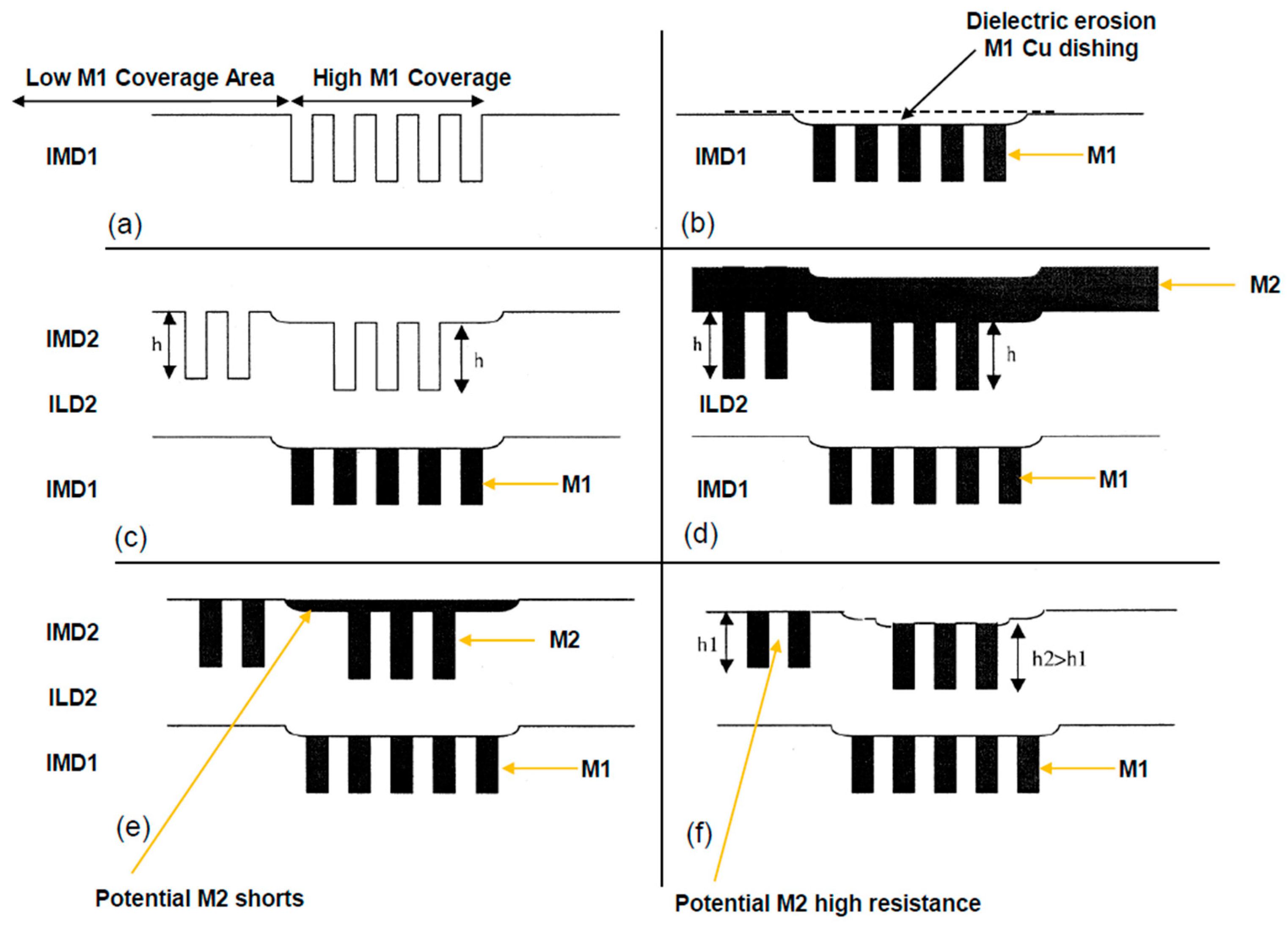
Similar to the problem described for M1 regarding low AA coverage area (with STI dishing), dual damascene integration can also accumulate non-planarity from previous metal layers. CMP at each layer at the BEOL can eliminate some of the non-planarity. However, for severe cases, or in the absence of an intermediate dielectric CMP, the topography created by pattern-dependent polishing is transferred to the next metal level [
16]. This is illustrated schematically in
Figure 19, showing the topography along different process steps. The IMD deposited after copper CMP on the lower level is conformal with the underlying surface profile. The non-planarity persists after dual-damascene patterning, etch, and Cu plating. It is subsequently removed during the initial stage of the copper CMP (bulk Cu removal). When the copper is removed completely from the raised areas on the IMD, some copper and mostly Ta/TaN residues remain in the depressions created by dishing and erosion of the underlying layer. Further CMP to clear the residue can cause the lines on the raised regions to suffer from over-polishing. The resistance of a dual-damascene conductor is therefore determined by a complex interaction of its layout environment on both the layer being polished as well as the underlying layers [
16].
Figure 19 provides further explanation of the process integration.
The effect of the multilevel metal coverage on resistance was demonstrated by the Tower team ([
29];
Figure 20) using a dedicated test chip that was internally designed with three separated long M5 resistors, and with two configurations—without any M1–M4 dummies underneath, and with dummies that had a coverage of 36%. The lack of dummies increased the resistance by around 40% in all three cases. In addition, the resistance distribution was almost doubled, as the height of the copper line strongly depended on the Cu CMP over polish. Note that
Figure 20 refers to resistance (not sheet resistance). The differences in resistance between the three different structures are related to the layout of the test chip (different length of connection lines) and not to coverage dependency or process effects.
The sheet resistance of Cu lines depends on three layout factors that affect both the overall thickness and the line CDs. The following are the result of a systematic experiment that was done in order to characterize each of the factors (see
Figure 20):
The above data enable us to predict with high accuracy what the effective sheet resistance will be based on the three dependencies listed. For example (
Figure 20d), an experimental comparison of two resistors with the layout and coverage conditions listed in
Figure 20 showed [
29] (i) for M5 resistor, with vs. without any metal coverage at M1–M4, the
K1 is ≈1.176 and (ii) for a very high M5 local coverage, due to the 7 µm line around and with space of 0.2 µm (97% local coverage),
K2 is ≈1.27. To account for both dependencies,
K1 ×
K2 = 1.176 × 1.27 = 1.49, which is close to the experimental result of 1.54. The difference may be related to the fact that the
K2 chart was not normalized to yield 1 at a local coverage of 45%.
9. Design for Manufacturing Copper Lines
Based on the dependencies described in
Section 8, we developed some guidelines in an attempt to minimize the defectivity and reduce variability. These guidelines can be easily coded to recommend layout rules and/or can be implemented in the Place and Rout (P&R) tool.
The first guideline is for checking the coverage around sensitive signal lines. The coverage limits can be much tighter than the platform limits. Another option is to check the metal coverage of the metal line below. However, in many cases, the routing is done automatically by the P&R tool, which is limited by the number of boundary conditions.
The second guideline is related to the high potential for metal shorts between two lines, due to poor planarity of the metal layers below, as explained in
Figure 19e. A larger space is recommended between two lines that cross above a high coverage metal area located below. The coverage of the metal underneath is checked and, if the coverage is above the recommended limit, the space between the two lines above should be increased.
The third guideline is related to the metal line width, which should be greater if the line crosses a locally low coverage area (<M.C.3) or high coverage area (M.C.4), measured in a small window (smaller than platform rule, M.C.3/4). This wider line is needed to support the photolithography process that will have limited DOF due to the poor planarity.
10. Different Methods for Dummy Fill Insertion
10.1. Dummy Shapes, Tools, and Insertion Efficiency
In mature technologies (65 nm and above), dummies are relatively large polygons that do not get any optical proximity correction (OPC) to save computing resources. However, for advance technologies, such as 28–14 nm or lower, with a very high density of dummies that have strong proximity to the drawing data, the dummies should also receive OPC to achieve a high design accuracy [
30].
The dummy fill polygons can have different shapes and spaces that set the density. The simple polygon has a square shape placed in a simple array or staggered array fill pattern. More complex dummies are based on a donut having an octagon shape or a multipolygon as an octagon donut with a square dummy inside. For some of the methods, like single-size dummy insertion or rule-base dummy insertion, the regular DRC tools can also be used. For more advanced insertion methods, more sophisticated tools are needed [
31].
There is no formal method to quantify the insertion efficiency. One simple way might be to compare the number of DRC violations before and after insertion. However, this method does not provide any information on the average and distribution of the coverage for proper support of the CMP processes. Here, we propose a simple expression for insertion efficiency (or “insertion yield”):
where
and
are the coverage at each window located at the design at
ij coordinates after and before insertion, respectively;
is the desired average coverage, and at many cases is set as 0.5 × (M.C.3 + M.C.4).
10.2. Single-Size Tile Filling
The first and most simple way of automatic pattern generation was noted first by Mentor Graphics [
32] and later on together with TSMC [
33]. The basic fill algorithm consists of the creation of a full array of dummies, followed by the elimination of dummies that are in violation of the manufacturing design rules. The main steps are as follows:
Step 1: Drawing data.
Step 2: Creation of a blindly flat cartesian array of dummies, based on the following inputs: dummy width, length, and space. For example, a tile array having W × L = 0.8 µm × 0.8 µm and 1 µm spacing will have a coverage at large “open area” of
Step 3: The original data are sized-up by the minimal space of the drawing data to the dummy. The output is the “no-fill area” that dummies should not overlap with.
Step 4: In the dummy array, dummies that overlap with the “no-fill area” are clipped and dummies within the no-fill area are removed.
Step 5: Any dummy with an area below the minimum as defined by the IC manufactures (see rule DM.A.1) is removed. An alternative is to remove any dummy that interacts with the “no-fill area.”
Another option in Step 1 is to scan the design for local coverage through a stepping window, e.g., with dimensions of 500 µm × 500 µm and a step of 250 µm. Later, dummies will be included only in windows that have an initial coverage below the minimum specified by the IC manufacturers (M.C.3). Step 3 is as above, and in Step 4, any window with a coverage > M.C.3 will also be part of the “no-fill area.” Step 5 would remain the same.
This simple method is the one used in 0.25–0.13 µm technologies for AA, GC, and Al BEOL. However, this method often adds more fill than necessary. This is due to the single-sized tile and the algorithm that does not take into consideration the initial local coverage nor the coverage gradient between two neighboring spots. The impact on timing might be significant.
10.3. Rule-Based (Linear-Programing) Dummy-Fill
Rule-based tiling is based on the STI dielectric thickness being directly proportional to the local pattern density. Hence, the physical design rules require a local pattern density as listed in
Table 1 and
Table 2.
Wherever there is an open space large enough, tiles should be inserted to increase the local pattern density within the bounds [
34]. The density rule can consider a single layer only, or a multilayer (one or even two layers below), in order to eliminate the introduction of tiles over sensitive signal lines or RF devices located below or above. However, the multilayer approach yields many cases of unfilled locations.
The basic fill algorithm consists of a local coverage calculation followed by a selective tile insertion at each window. The last step is to eliminate the dummies that violate the IC manufacturers’ design rules.
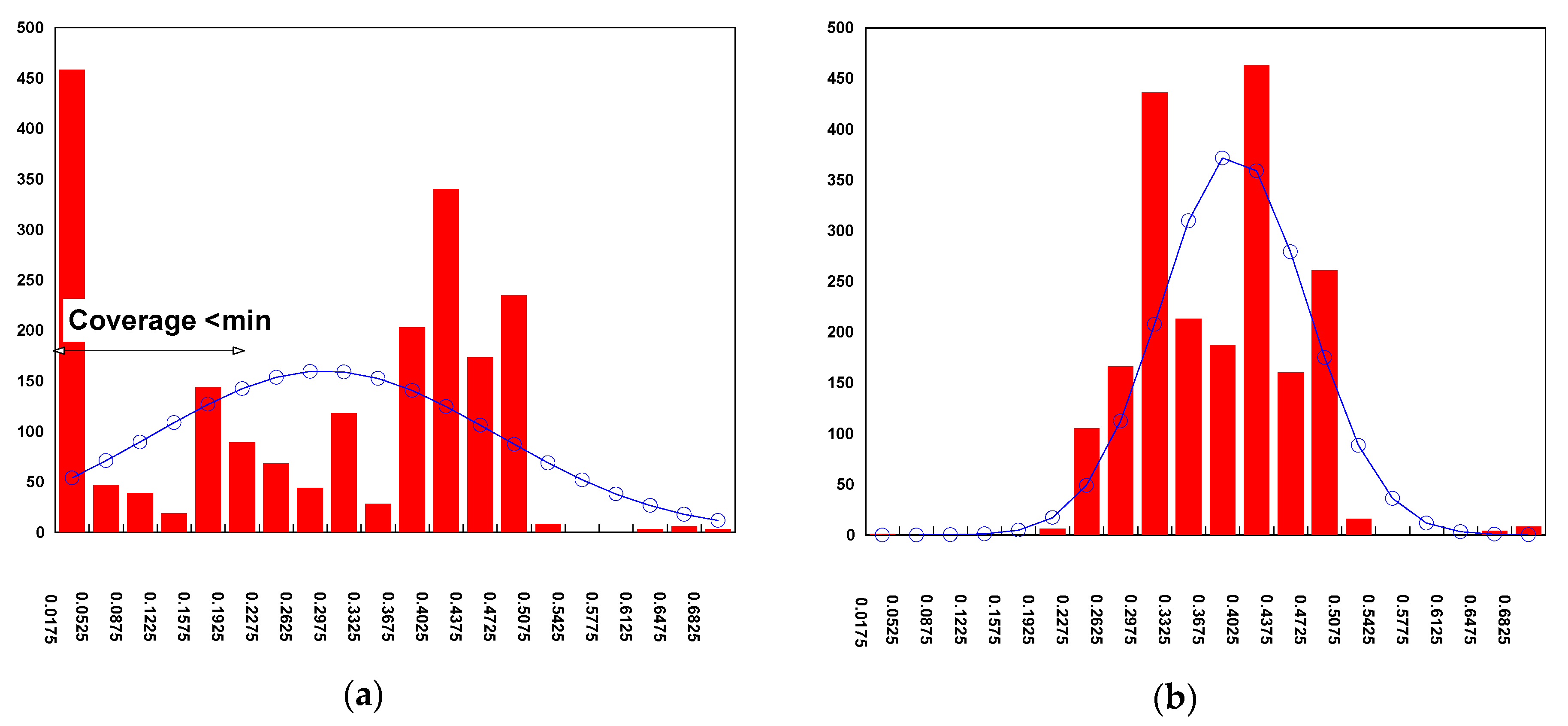
Figure 21 shows the coverage density of the M1 layer before and after the dummy fill. All windows that have no metal (around 25% from the total chip area) and violate M.C.3 would now be filled. The statistics before filling showed an average coverage of 26% and 1σ of 17.7%. After filling, the average goes up to 36% and there is a much tighter distribution across the chip, with 1σ of 7%.
Another similar approach is the minimal variation method [
17,
35], which seeks to maximize the minimal window density. The method first calculates the effective density of the layout based on the local coverage and the material thickness after CMP (based on the CMP model). It then calculates a target-effective density as the mean of the effective density. Based on the difference between the local effective density value and the target effective density value, tiles are prioritized and several are selected simultaneously for filling. The method then assigns dummy features in low-effective-density areas or removes the already filled dummy features from high-effective-density areas. The process is repeated until the uniformity of the effective density cannot be further improved or until the maximal number of iterations is reached [
17]. Based on the maximum density coverage (M.C.4), defined by the IC manufacturers, the dummy tile inserted in any window is defined [
35]. Then, the minimum variation formulation seeks to maximize the minimal window density. A detailed mathematical explanation on the minimum variation interactive method can be found in [
17].
The dummy fill method is optimized by adjusting the settings for the tile dimensions and space for each type of dummy. The goal is to achieve high insertion efficiency, that is, to eliminate spots with low coverage and without dummies due to fine drawing lines having space that is slightly below DM.W.1 + 2 × M.S.1 (see
Table 3).
Figure 22 shows an example of an optimized dummy fill run-set, with several different sizes of square tiles. The IC (integrated circuit) is a full analog-specific IC (ASIC) including a large array of single port SRAM (SP-SRAM), several blocks of standard cell libs, several analog modules, and a phase shift lock (PLL) in an overall area of 5.5 mm × 5.5 mm. The chart shows the coverage before and after filling for every window. The solid line represents X = Y, so each point on the chart is a window with or without dummies.
The main success criteria of the dummy fill run-set optimization are as follows:
All windows that are below the minimal local coverage must include dummies with a coverage ≥ M.C.3,
All windows that have a coverage close to or above M.C.4 should not receive any dummies.
The overall coverage distribution after filling (see
Figure 21b) should have an average that fits with the polishing process. In addition, the distribution should be as tight as possible. From a practical point-of-view, the insertion should be differential, i.e., windows that are 1–5% higher than M.C.3 should have relatively large tiles with small spaces in order to increase the coverage. However, windows that are very close to the target or even slightly above the target should get relatively small tiles with large spaces to minimize the coverage increase or should receive no tiles. The optimized run-set yielded insertion efficiency of 56% and was achieved by carefully setting the distance between dummy metal tiles to metal lines at the same level and above or below. A larger distance minimizes the coupling capacitance but may yield limited increase in coverage.
The run-set should block the insertion of tiles based on a predefined list of marking layers (blocking layers).
It should require minimum CPU resources, minimum running time, and not too large GDS file size after filling. Too large a file size will slow down the mask data preparation (MDP)/optimal proximity correction (OPC) process, the reticle enhancement technique (RET) activity, the file transfer to the mask shop, and the fracturing, among others.
For 20 nm technologies and below, the run-set should be able to support design with DP (double patterning) and TP (triple patterning). See, e.g., the work of the Samsung team, for a M2 layer with a self-aligned DP (SADP) process [
36].
Figure 22a is our example for optimized filling with 56% insertion efficiency, and in it, we also explain “differential filling,” that is, high coverage tiles with a low coverage window and low coverage tiles (or no tiles) for high coverage windows.
Figure 22b shows an example of a non-optimized insertion run-set with an insertion efficiency of only 21.9%. To eliminate performance degradation due to fringe capacitance between the dummy lines and the drawing metal lines, the boundary condition for M2 insertion was set conservatively, by keeping 3 µm from drawing M2 metal lines and 1 µm from drawing M1 and M3 below or above, respectively. As a result of this “stack fill consideration,” a large amount of low-coverage windows did not fill and yield M2.C.3 violations.
Figure 22c is another example of non-optimized insertion, with an efficiency of 39%. Some of the 12 tile types were set to be long rectangles, not squares, with a small space. The idea was to fill areas that need special shapes or orientation to maximize the fill density. However, the results showed a lack of coverage in many windows. The optimization process repeated with different scenarios and included at least 10 different ICs for different applications as the amount of blocking layers depend on the % of analog, RF, and other sensitive circuits that have a tight specification of timing. Products with different area sizes were also selected. The same optimization and QA were used for the cases when the dummy fill was done by the P&R tool.
The foundry test element group (TEG) or technology qualification vehicle (TQV) dedicated a mask-set that included all test-chips for technology calibration, and qualification could not be used in most cases due to the large difference in overall topography compared to a regular IC. This was due to the many test chips and the number of bonding pads, which were not proportional to the IC area/application. Furthermore, many types of devices were grouped and placed in one area and were almost not included in other areas.
Another criterion of success is that long conductors of the same metal level will have an identical (and minimal) coupling capacitance induced by the dummy tile. One of the ways to achieve this is to set the filling utility to not be on a regular grid but include an offset in both x and y directions that breaks the symmetry of the pattern. This offset also simplified the photolithography process by eliminating false alignment during wafer setting at the stepper or defect metrology tools.
Figure 22d is an example of the popular dummy shift.
Figure 22e presents a shift that also has the advantage of having the same fringe capacitance as any horizontal and vertical lines located nearby. More complex tiles (cell-based) are described later in this paper.
Another important success criterion for optimal filling is the coverage gradient between each window and the surrounding neighbors (M.C.34). If there is too great a difference, then it impacts the polish rate and may yield metal residues with high potential for shorts.
Another method for the dummy metal fill was proposed by the team from SMIC [
37]. Their method was based on the fact that both the total pattern perimeter and the pattern density control the final topography. For the same local coverage, patterns with a longer perimeter will have smaller height differences.
10.4. Model-Based Driven Dummy Fill
Model-based methods provide more accuracy and efficiency [
34]. The method is based on analytical expressions formulated above (see
Section 2.6) and describe the relationship between local patterns and ILD thickness. The method used a CMP model to identify locations (hotspots) where planarity was worse. Examples for CMP models are listed in [
6]. The initial oxide density is not only proportional to the local pattern but also can be calculated as the summation of weighed local pattern density within a weighting region. The size of the weighting region depends on the CMP processing, similar to the CMP range. Based on these models, a two-step solution for dummy feature placement is proposed as follows: first, the minimum variation should compute the number of dummy features required in each small window. Second, place the calculated amount into each rectangle while optionally optimizing certain local properties. The team from TSMC used a similar approach but with some modifications [
18]—their first two steps were similar, but they used a random generator to choose the pattern type such as rectangles, stripes, etc. In contrast to the Tian method [
34], which uses square dummies to easily handle cases with vertical and horizontal lines, TSMC’s approach uses a randomized-shape dummy feature, thereby a spatial signature produced by the dummy feature will not be presented in the whole chip layout. Using this method, the mean coverage increased from ≈30% to ≈65%. Analysis of the coverage histogram before and after filling showed that the number of windows that had low coverage (<M.C.3) was reduced drastically. However, some sites were still below the minimum. The density histogram also shows many windows that used to be <M.C.4 before the fill but violated the maximum rule afterwards.
For STI CMP, the team from Motorola used model-based filling and reduced the within-die thickness variation by >50% compared to the rule base [
38]. They used two types of tiles, i.e., “background” tiles that have a small feature size and pitch (≈50%), with the ability to have high yield of insertion, and the second tile that was 10 µm × 10 µm for large open regions.
10.5. Net-Aware and Timing-Aware Dummy Metal Fill
A dummy fill can have undesirable impacts on the net capacitance yield path delays. An estimation for the timing impact of a 65 nm design is ≈4% [
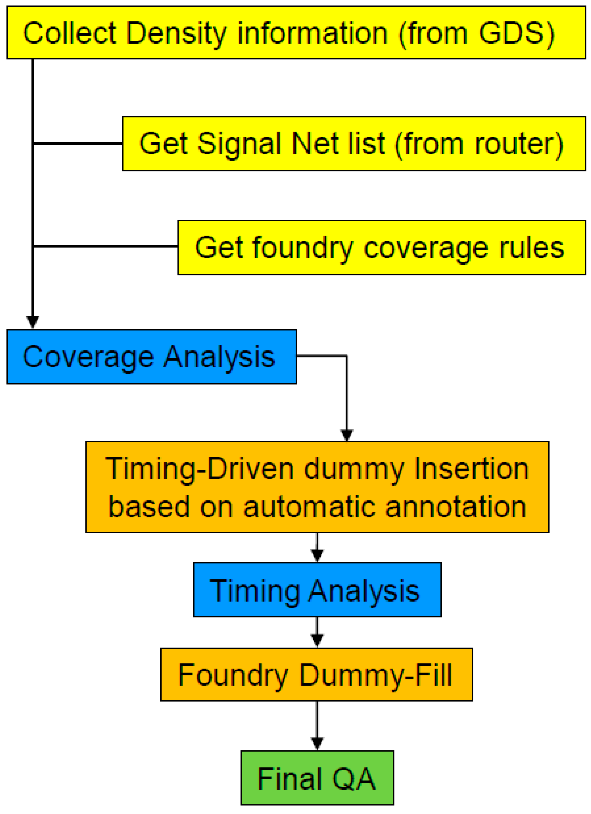
39]. A timing-aware (automatic annotation) track fill insertion flow, which was proposed by a team from the foundry Chartered (now GF) and Magma, consists of dummy fills by the router. The flow is shown in
Figure 23. First, the routed database feeds into the router, which analyzes the density violations based on the density rules. After detecting the locations of density violations, a timing engine is invoked to do timing analysis while inserting the metal fills. The insertion is into the standard cell area only and will not touch any other IP (intellectual property) area or IOs (input/output). Based on that, we can set a ground-rule that inserted dummies near critical signal lines will have larger spaces than noncritical lines: ≥2–3 µm for clock paths and even ≥5 µm for critical paths. Finally, the timing was analyzed again to ensure performance was acceptable. The next step is to use the manufacture insertion utility to complete the coverage needs around IPs, IOs, and the overall IC. Using this hybrid approach, there is a minimal impact on design trimming with a uniform coverage across the IC. For the design of 65 nm technology with an area of 9 mm
2, the maximum slack degradation value was improved from −101 psec (for the case of using only the foundry insertion utility) to −19 psec with the hybrid approach.
A different and simpler work flow was proposed by the team from SEMTECH [
40]. The workflow can prevent fill insertion around identified nets by setting larger space requirements or by removing inserted tiles around identified nets. The manufacturer insertion utility was also used.
A floating fill, in comparison to a grounded fill, offers a smaller increase in the total capacitance and does not require power/ground routes for the fill geometry. However, a floating fill increases the coupling capacitance, which can cause signal integrity issues. A ground fill, despite its larger impact on the total capacitance and high routing costs that often lead to ECOs (engineering change orders), can be used as a substitute [
41]. Shielding is widely used in integrated circuits to mitigate cross talk between coupled lines. In “passive” shielding, the power/ground (P/G) lines are routed as shield lines between critical signals interconnects to minimize the noise coupled from an aggressor to a victim line. Inserting shield lines between the aggressor and victim lines reduces the capacitive and inductive coupling between adjacent blocks [
42]. It is difficult and consumes resources to connect the shield to the reference net. However, the metal fill can use whatever resources are left over and minimize the impact. This approach was experimentally tested by Intel [
43] and yielded promising improvements.
10.6. More Advance Fill Methods—Cell Fill
The cell-based fill method was introduced by CSR and Mentor Graphics for 28 nm technology and below [
44]. The cell uses several layers to handle multilevel density rules. For the FEOL, the cell consists of AA and poly to support the coverage needs around MOSFETs. For the BEOL, the cell includes all metals and vias in the design to generate a fine metal grid with vias in between metal lines, which also supports the via coverage rules listed at the manufacture DRM. The cell fill can be followed with other rule-based or model-based fill shapes that have the advantage of higher fill insertion (vs. the cell fill).
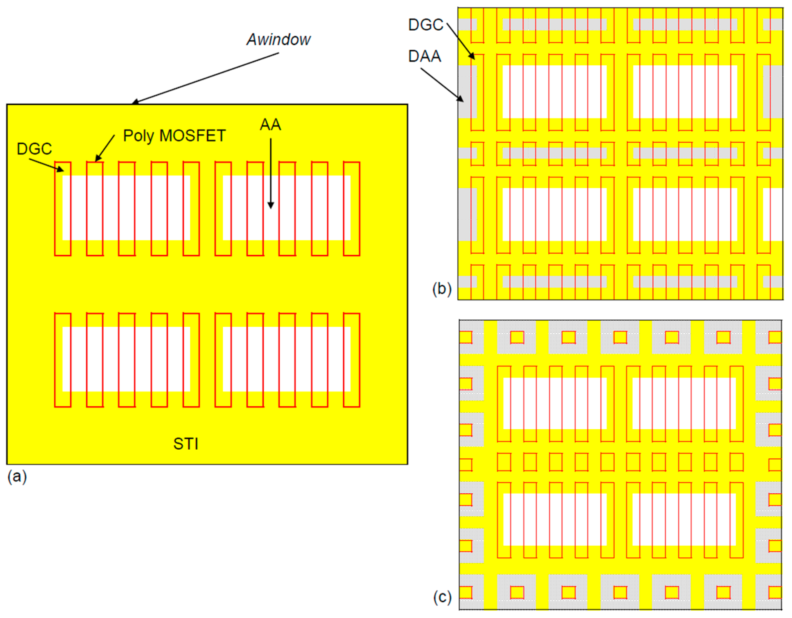
Figure 24 shows examples of cell fill for the FEOL and BEOL. To support DAA and DGC density DRs, the cell is like a typical MOSFET but without any contacts, to eliminate conflicts with M1. All DGC lines have a fixed width and a fixed pitch, as required by the regularity DRs. The placement of two cells is without any space in between. For the BEOL, two options are shown with the same metal layers and vias in between. The first option has higher metal coverage. However, the second option, as the metals at adjacent cells are not touching each other, has the ability to “shift” cells in case a cell is placed near a signal or a clock line.
10.7. Capacitive Coupling of Dummies
The capacitance of a signal line located in between two dummies and over a single ground plane can be calculated as a function of DM.D.1. The calculation can use textbook equations (e.g., [
45]). Based on such a dependency, we can define a simple rule-of-thumb for DM.D.1: >~25 × M.S.1 (minimum metal–metal space). In fact, the exact value can be set based on the dummy length and the parallel length with the signal line (a large dummy size should have a larger space compared with a small dummy).
The team from Renesas [
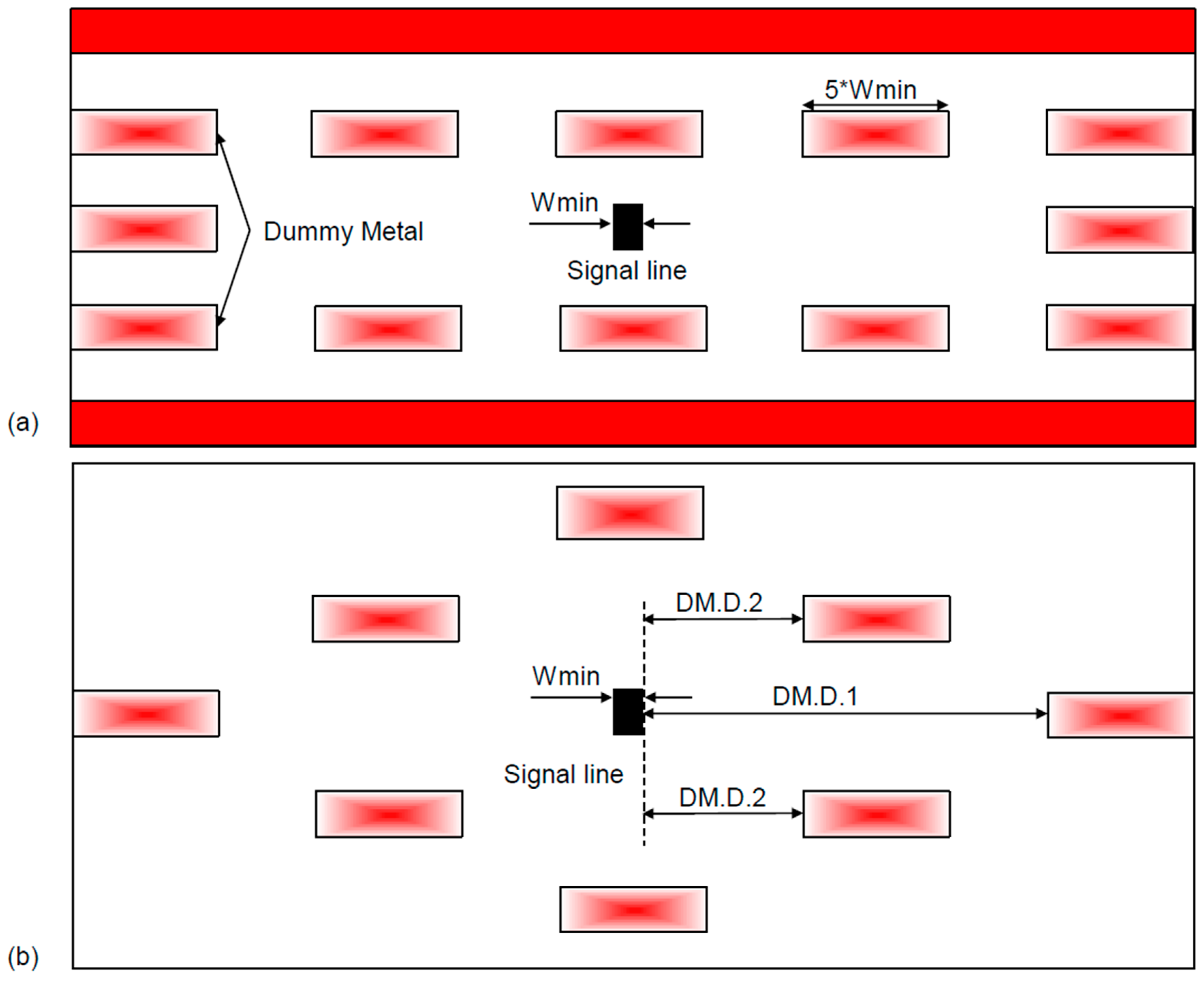
46] analyzed the impact of the dummy fill on parasitic capacitance by employing a 3D field solver, with intermediate layer parameters based on 90 nm technology. Their first example (
Figure 25a) was a signal line located at Mi, having unrelated routing layers at Mi − 2 and Mi + 2. Dummy metals were located on Mi − 1, Mi, and Mi + 1. The capacitance of the signal line with dummy fill increased by 15–35% for a dummy density of 20–70%. Note that no dummy neighbors were located around the metal signal at the same metal level. Therefore, the increase in the capacitance was from the dummies above and below (see rule DM.D.2). Their next example was for the coupling capacitance with a dummy fill between signal lines (
Figure 25b). When the distance between the signal line and the dummy metal (DM.D.1) was ≈Wmin, the capacitance of the middle signal line went up by around 60%, and for DM.D.1 = 10 × Wmin, the capacitance went up by only 20%. This demonstrates the “insertion priority,” that is, a large DM.D.1 is more important than DM.D.2.
Kahng et al. [
41] also studied the impact of various floating fill configuration parameters on coupling capacitance such as fill size, fill location, distance from interconnect edges, and multiple fill columns and rows. Using this information, we can list a set of guidelines as follows:
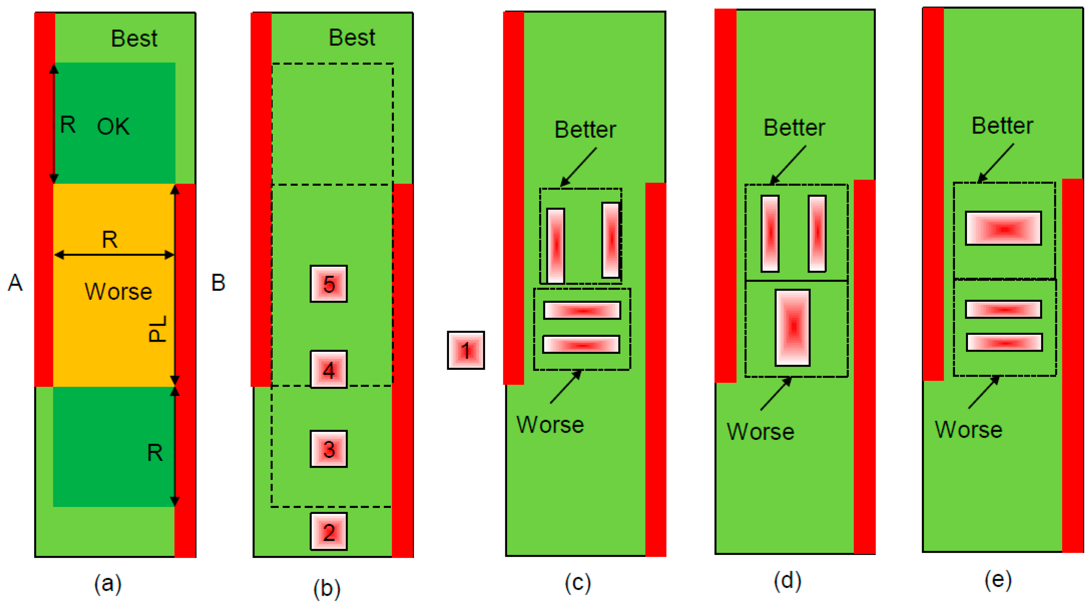
Guideline 1—tile location: For lines A and B (
Figure 26a), the coupling capacitance is only affected by dummies located at the area defined by the (metal space) × (parallel length + 2 × metal space). It is best not to place dummies between the two lines and far from the parallel length area. Insertion close to but outside the parallel length is possible. However, the area defined by the parallel length will yield the highest coupling capacitance. The relative change in capacitance for the five locations shown in
Figure 26b is ×100 for location #2 (compared with location #1) and ×380, ×414, and ×376 for locations 3–5, respectively.
Guideline 2—tile orientation: For a dummy inserted between two lines (
Figure 26c), it is better to have a narrow and long tile located along the lines. The worst-case scenario is to have wide and short tiles.
Guideline 3—tile width: For dummies along the lines (
Figure 26d), it is better to have several thin dummies than one thick dummy. The dummy width should be DM.W.1, allowed by DRs with a maximum number of dummy columns. For the same tile area and coverage, it is better to have a centralized long tile with a minimum width.
Guideline 4: For dummies perpendicular to the lines (
Figure 26e), it is better to have one thick dummy than several thin dummies; minimize the number of dummies rows.
Guideline 5: Large width wires are more susceptible to increased capacitance due to fill. It is preferred to have thinner wires around dummies.
Similar work was done by the team from Synopsys [
47] for 32 nm DRs.
10.8. The Effect of Dummy Filling on Wire Resistance and Inductance
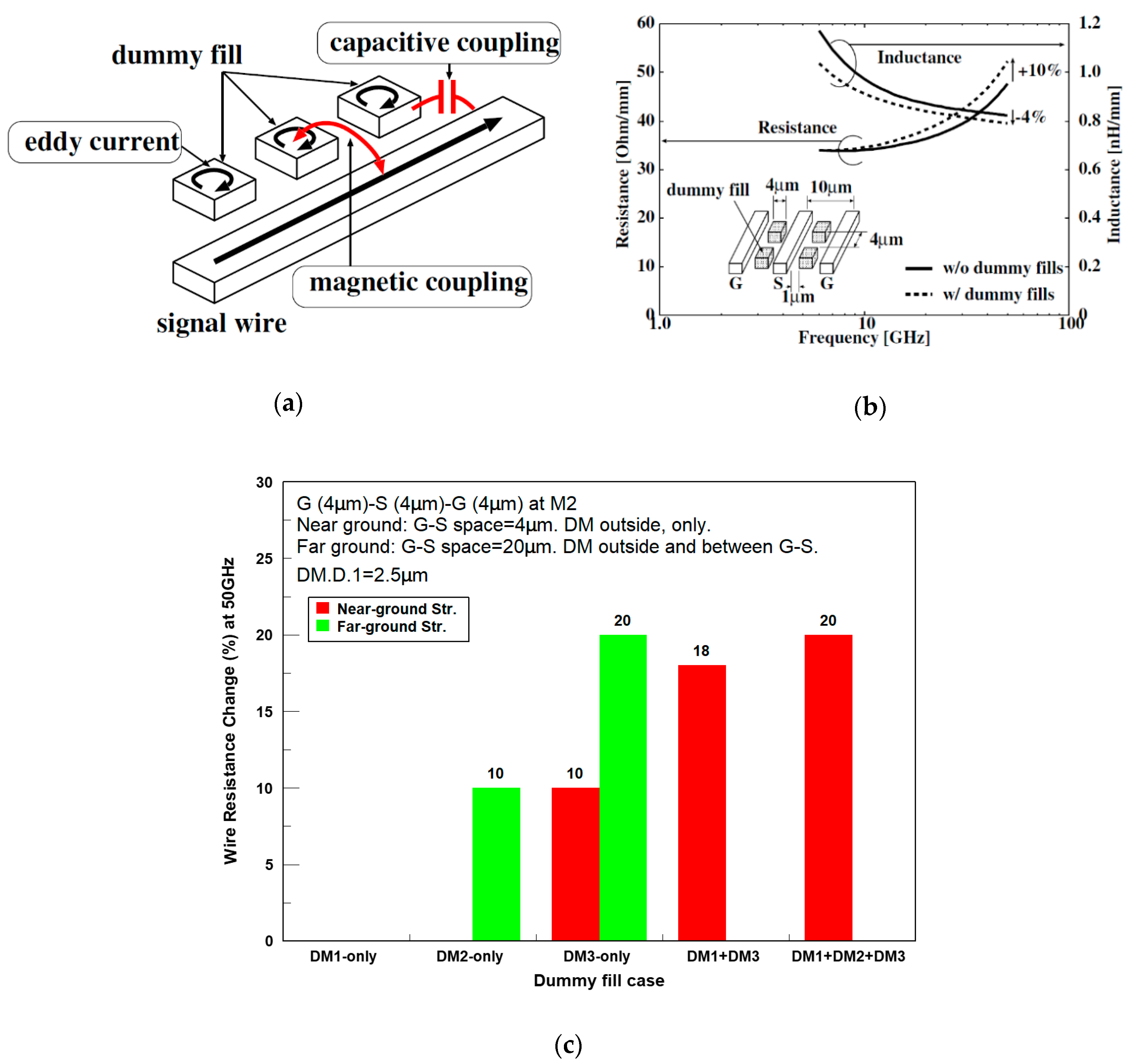
Since the dummy fills are floating conductors, the current flow in the dummy is negligible at low frequencies. However, at high frequencies, the eddy current induced in the dummy fills becomes significant (
Figure 27a) and increases the resistance and magnetic coupling between the signal wire, while it decreases the wire inductance. The team from Kyoto university performed a detailed study [
48,
49] of this.
Figure 27b shows an example of the 3D field-solver frequency characteristics of a G–S–G (Ground–Signal–Ground) coplanar transmission line (TL). For the TLs with the dimensions listed in
Figure 27, the difference in resistance becomes larger at higher frequencies, at 50 GHz, and the resistance increases by around 10% due to the eddy current in the dummy fill. In terms of the inductance, the effect of the dummy fill is relatively small (<4% at 50 GHz).
The effect on the ground wires was also evaluated using a near-ground and far-from-ground structure with M2 G-S-G wires of 4 µm width and spacing. For this structure, the dummy metals were located only outside the GSG. The far-from-ground structure had 20 µm G–S space and dummies in between the wires as well as outside. In all cases, the dummy tiles were 2 µm × 2 µm, staggered, with a local density of 36% and placed with DM.D.1 = 2.5 µm. The resistance change compared with the case without dummies at 50 GHz is shown in
Figure 27c. For the near-ground structure, the resistance change began at >10 GHz and for the far-from-ground structure, it began at >20 GHz. For both cases, the dummies at M1 and M3 have a big impact on the resistance. The adjacent ground wires (near-ground structure) can shield the effect of the dummy fills in the same metal layer. However, the ground wires cannot suppress the effect from the upper/lower dummies [
48].
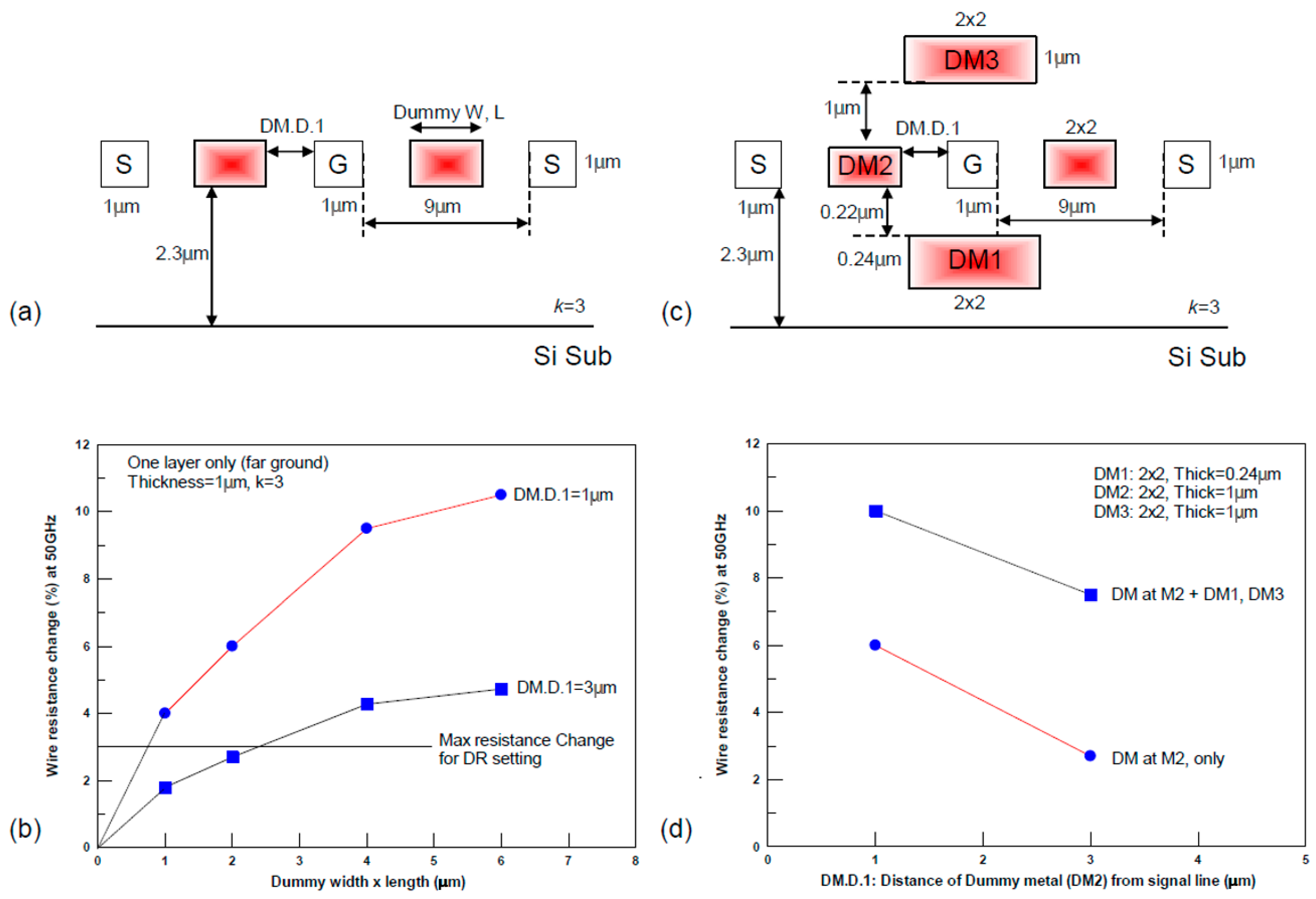
The effect of dummy size and distance of a dummy from the signal line (DM.D.1) was also analyzed [
49].
Figure 28a shows the far-from-ground structure that was used with different sizes of dummy tiles and with DM.D.1 of 1 and 3 µm. As the dummy fill size became larger and distance from the line decreased (smaller DM.D.1), the resistance increased (see
Figure 28b). Using these data, we extracted a related DR to be used by the insertion utility—for high-speed applications, assuming ΔR% ≤ 3% as a success criterion, DM.W.1 should be ≥0.8 µm × 0.8 µm for DM.D.1 = 1 µm or ≥2 µm × 2 µm for DM.D.1 = 3 µm.
The multilevel effect of the dummies checked by the structures can be seen in
Figure 28c. The far-from-ground structure also included DM1 and DM2 dummies below and above, respectively, with the shown dimensions. A signal line thickness of 1 µm is typical for semi-global lines at 65 nm technologies and below. Due to the magnetic coupling, the eddy currents flow in the dummy tiles in the upper and lower layers. The increase in resistance (
Figure 28d) is almost doubled by the dummy fills in the upper and lower layers. Since the thickness of the ILD is relatively smaller than DM.D.1, the effect of the dummy fills is significant [
49]. Using these data, we can define a guideline (DR) to be used by the insertion utility—for high-speed applications, signal lines should not have dummies below and above them. In addition, DM.D.2 should be set to at least 15 times more than the ILD thickness.
10.9. The Effect of Dummy Filling on Inductors
For passive devices in RF circuits, the quality factor (Q-factor) parameter is defined as the ratio between the energy stored to the energy dissipated per cycle. The higher the Q-factor, the lower the loss of a passive device. To maximize the Q-factor, the inductor is made using the top metal layer (to minimize capacitance coupling), which should be as thick as possible to minimize resistance. Based on this, any dummies around and below the inductors will degrade the Q-factor.
The team from Tower calculated Q-factor degradation due to inductor thickness reduction. The results were for a symmetrical inductor made using 3.3 µm Cu metal. An example for thickness reduction in this layer due to dishing is seen in
Figure 4c. At 2.7 GHz, every 1% reduction in thickness represented about a 0.33% degradation of the Q-factor [
50].
Dummies located near or below the spiral inductor increase the capacitance and reduce the self-resonant frequency. In addition, for high frequencies (>10 Ghz, see
Figure 27b), the eddy current in the dummy fill becomes significant. The eddy current (see
Figure 27a) increases the loss and the magnetic coupling between the signal current and decreases the wire inductance [
51]. A typical spiral inductor is seen in
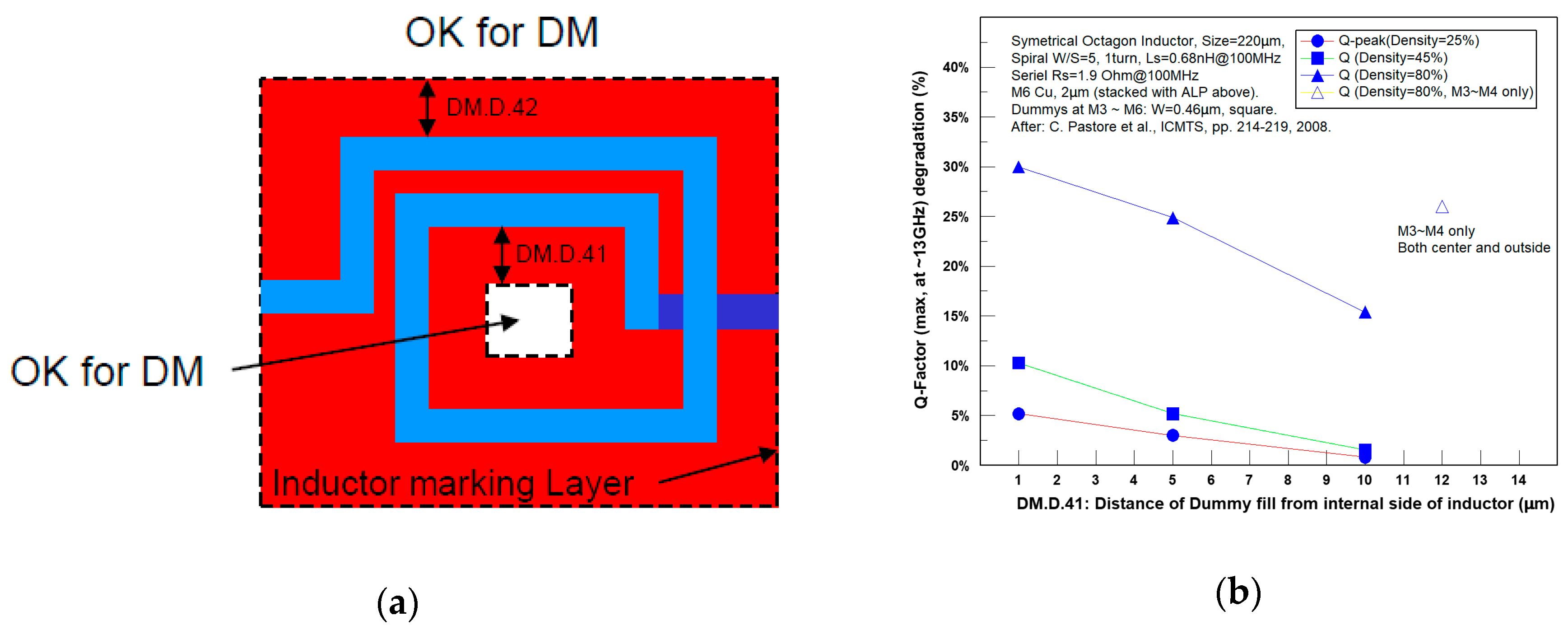
Figure 29a. Dummies can be placed outside the inductor and possibly also at the center, but in both cases should not be overlapped with the inductor marking layer ring. DM.D.4 is the enclosure of the marking layer around the inductor.
The team from STMicroelectronics [
52,
53] reported results of a systematic work that checked the effects of dummies located at the center and below Cu inductors. The process included six Cu layers and the inductor was located at M6, stacked with the Al layer above, which was used for bonding. M3–M6 square dummies with a fixed width of 0.46 µm and a density of 25–80% were inserted at the center of the spiral, keeping a DM.D.41 of from 1 to 10 µm.
Figure 29b shows the results. For a low density (25%), DM.D.41 had a limited effect on Qmax degradation. However, if an aggressive design rule was used (80% density, DM.D.41 = 1 µm), the effect on the Q-factor was drastic, with a 30% degradation in Qmax, due to the increase in the parasitic capacitance. At any density, high DM.D.41 led to less degradation, and in many cases, it was set to 30 µm or more. Analysis showed that the configuration of the dummies—stacked or crossed—had little real effect. Having dummies only below the inductor (M3 and M4 only) did not yield a significant improvement in Qmax. A later work from STMicroelectronics [
53] analyzed the Qmax degradation considering dummies located both at the inside area (set by DM.D.41) and outside area (DM.D.42) of the inductor, with similar density. Qmax degradation was almost doubled with a similar sensitivity to the distance of dummies inside and outside. Based on that, we recommend a single value for DM.D.4. The stacked configuration of the dummies under the inductor (aligned or crossed) was found to be a negligible factor on the Qmax.
The orientation of the tiles at the inductor’s center is not an important factor; this was experimentally verified by the team from Philips [
54]. To maximize the Q-factor, the dummy size should be kept small (<3 µm × 3 µm). Using 10 µm × 10 µm dummies degraded the Q-factor by around 10% compared to the case of 3 µm × 3 µm dummies [
55]. Smaller dummies mean smaller magnetic coupling with limited flow of eddy currents and limited Q-factor degradation. Recently, the common team of GLOBALFOUNDRYS and Mentor Graphics reported [
56] on orientation-aware dummy fill that was mostly made to enhance inductor performance at the 14 nm platform by a symmetrical filling. All of these data have been used to set dummy rules related to inductors.
10.10. RTA-Aware Dummy Fill Insertion
Rapid thermal annealing (RTA) is widely used during FEOL manufacturing to reduce the overall thermal budget and ensure that there are shallow junctions with high activation. The high temperature annealing time has gradually reduced from seconds, using halogen lamps, to milliseconds by flash lamp anneals (FLA). The first reported work on inter-die variation of CMOS inverter delay correlated the millimeter scale variation in the device reflectivity with the pattern density [
57]. In that study, a shift of >15% was observed in the sheet resistance of an unsalicided polyline located over the STI at different coverages. The larger the STI exposed area around the poly resistor, the higher the effective temperature that improved the dopant activation and reduced the sheet resistance. Additionally, the faster the temperature ramp rates, the higher the variation was, due to the higher dependency on the thermal diffusion distance at the wafer surface, as explained below. The mechanism for RTA involved heating the top-side of the wafer surface by exposure to an array of lamps that was pulsed rapidly to transfer radiative heat to the wafer surface [
58]. However, during this time, the entire silicon substrate does not reach thermal equilibrium due to the extremely short heating period. The surface emissivity of various material stacks determines the amount of absorption energy and the final annealing temperature. As a result, different layout pattern densities lead to different annealing temperatures and device characteristics. The length scale of such variations is determined by the thermal diffusion distance in the wafer surface, which is proportional to
, where D is the thermal conductivity of silicon and
t is the annealing time. In millisecond RTA processing times, the typical length is around hundreds of microns. This is one of the parameters used to define a window size for analysis, as will be explained later. As an example, researchers from IBM [
59] analyzed a realistic layout of a 45 nm test chip. Due to the layout style, various components exhibited a pronounced difference in pattern density. By the thermal simulation tool, the fluctuation in the annealing temperature which directly induced threshold voltage variation by more than 30 mV could be seen. The largest difference was observed close to the boundary of different components, where the non-uniformity of the circuit layout reaches the maximum.
The team from TSMC [
60] checked how to optimize the emissivity uniformity for the FLA process by DAA filling. The emissivity for the STI, AA (N+ or P+), Poly over STI, and Poly over Gate oxide are 0.80, 0.43, 0.46, and 0.55, respectively.
To minimize the temperature variation, the “equivalent emissivity,” which takes into consideration the emissivity and the area of each location, is calculated as
where
n is the four locations described above and
εi and A
i are the emissivity and the area, respectively. To identify the appropriate window area (Awidnow), the team from IBM [
59] simulated a sample 45 nm design with various sizes of simulation window. The exact value depends on the RTA conditions, such as the annealing time and temperature. For the purposes of DR definition and dummy fill insertion, a typical window of 30 µm × 30 µm is reasonable.
For an “open area,” without any design data and before the dummy fill, the equivalent emissivity will be exactly 0.8, as the entire area is covered with STI only. After the fill with DAA (45%, for this example) and DGC located over STI (25%, for this example), the equivalent emissivity will drop to about 0.55. To minimize RTA variability, this number can be used as the emissivity equivalent “target” for windows in the design data. In
Table 4 and
Figure 30, we provide our example for the dummy fill insertion with consideration given to minimizing RTA variation. The original design had four MOSFETs organized in two rows. Each transistor included three fingers and a DGC at each side, to satisfy the regularity requirements. Different types of DAA were inserted together with DGC, which increased the coverage and reduced the equivalent emissivity. The optimal fill was achieved with a combination of a cell fill with a pattern of a MOSFET together with DAA rings, and a DGC placed on the STI at the center. The overfill of DAA or DGC would provide lower equivalent emissivity. However, this might violate the maximal coverage limits, as seen in
Figure 29b, where the poly coverage is close or above GC.C.2. Therefore, the insertion utility needs to use the equivalent emissivity calculation described, as an additional boundary condition to the coverage limits.
10.11. Dummy Fill Considerations for Design Fix (ECO Fill)
Due to the complexity of the dummy insertion for advanced technologies, any demand (or “order”) for engineering change (ECO) that arrives after the design has already passed the dummy fill insertion step will lead to a significant delay to tape-out. To overcome this, the team from TSMC [
61] developed an automated design flow for the 16 nm and below platforms. The inputs are the original design and modified (ECO) design databases, and the original dummy file database. The workflow uses the knowledge of the process layer/datatype mapping and DRC spacing as an input into the ECO fill utility. As an example, we assume that three bus lines located at M4 need to change place in the design. In a very general way, the two main tasks of the ECO fill utility are to fill the empty area with dummies where the bus lines were located and to remove existing dummies so the bus line can be replaced.
11. Metal Slits Rules
One of the ways to reduce copper coverage is to include metal slots (
Table 5,
Figure 31). For simplicity, a dedicated support layer is used to define the slot, e.g., layer M (slotting). During mask data preparation at the wafer manufacturer, and before OPC, the metal is “punched” by a simple Boolean operator. The slits are needed only for wide and long lines. A typical definition for a “wide” copper line is >10 µm width.
The impact of slotting on resistance can be simulated using 2D field solver to calculate the current distribution. Arora [
62] showed the impact of slots on wire resistance—a simple calculation showed that the increase in resistance is proportional to the area of the slots. However, at high operating frequencies, the resistance degradation was enhanced due to a skin effect. This is the reason for setting rule MSLOT.N.1 to eliminate slotting signal lines or inductors.
Figure 32 shows our electromagnetic simulation of different slit configurations and the resistance change [
63]. Using this example, and assuming all slits are placed parallel to the current flow, we can set additional guidelines for the insertion of slits:
Guideline 1: For the same overall slit area, it is better to have as many (per rule MSLOT.W.1) narrow and long slits as possible.
Figure 32(a.1–a.3) shows a resistance reduction from 17.6% to 16.1% to 15.2%, respectively. Narrow slits mean there will be lower current crowding, as shown in
Figure 32b.
Guideline 2: For the same overall slit area, it is better to have staggered placement of slits. Comparing
Figure 32(a.3,a.4,b.1,b.2) shows that there was a relative resistance reduction in around 7% due to this configuration.
Guideline 3: Eliminate having OPC to the slits, for having rounded slits corners. The increase in current density is the highest at the slits’ corners, so rounded corners would mean lower resistance. This guideline is easy to implement, as the slits are drawn using a dedicated support layer.
Guideline 4: Eliminate having slits that restrict the path of the current flow. Slits should be placed parallel to the direction of the current.
Figure 32(c.1,c.2) compare the current density for two configurations: having two slits in a row having current crowding at the slits corner (marked with arrow) and staggered slits configuration. The figure also shows the resistance reduction for the second case. This is the reason for rule MSLOT.N.2, which eliminates slotting at intersection areas. In many cases when using the slits insertion utility, the slit should be set to be a simple square to eliminate current blocking.
The effect of the slotting configuration on inductors’ RF performance was also studied by Blaschke [
50], who used detailed momentum simulations to analyze a range of configurations of metal slots for resistance and Q-factor dependency. As the Q-factor is directly proportional to the inductor resistance, a large slot area means high resistance and Q-factor degradation. It was found that the optimal configuration is to have one long slot located along the axes of the line. Breaking the single slot into several long or short lines, or staggered squares, degraded the Q-factor. For example, including a single slot of 1–3 µm width increased the line resistance by about 9% and degraded the Q-factor by about 9% (both compared to the case without a slot). However, using a staggered, square slot, increased the resistance by 9% but degraded the Q-factor by >14%. The length of the single slot is dependent on the wavelength, and a typical length should be <150 µm.
The effect of metal slits on the EM performance was described in detail in [
22]. For stress-induced voids reliability performances, the team from ONSEMI showed that the insertion of metal slots close to electrically active vias can act as a diffusive barrier and improved the via lifetime [
64].
12. Summary and Future Directions
The continuous scaling needed for higher density and better performance has introduced new coverage challenges reviewed in this paper. The global coverage rules have been replaced by local rules. In parallel, a new set of rules for dummy insertion were developed by IC manufacturers. Advanced fill insertion utilities are now considered in addition to coverage needs, along with thermal effects, sensitive signal line, and critical analog and RF devices like inductors and double patterning processes, among others. To minimize proximity effects, the simple “tile” was replaced with a “cell” consisting of several layers. It is reasonable to assume that future technologies will require tighter coverage limits and be multilayer based, as measured by smaller windows (of less than 10 µm × 10 µm). The inserted cells will be highly regular and have a carefully optimized layout for uniform coverage. Finally, new thermal rules will require a uniform layout with a tight equivalent emissivity range.
