High Temperature Oxidation Behaviors of CrNx and Cr-Si-N Thin Films at 1000 °C


1
Chemistry Division, Center for General Education, Chang Gung University, Taoyuan 33302, Taiwan
2
Department of Nuclear Medicine and Molecular Imaging Center, Chang Gung Memorial Hospital, Taoyuan 33305, Taiwan
3
Department of Mechanical Engineering, Tungnan University, Taipei 22202, Taiwan
4
Department of Materials Engineering, Ming Chi University of Technology, New Taipei 24301, Taiwan
5
Center for Plasma and Thin Film Technologies, Ming Chi University of Technology, New Taipei 24301, Taiwan
6
Department of Mechanical Engineering, Chang Gung University, Taoyuan 33302, Taiwan
7
Plastic and Reconstructive Surgery, and Craniofacial Research Center, Chang Gung Memorial Hospital, Taoyuan 33305, Taiwan
*
Author to whom correspondence should be addressed.
Coatings 2019, 9(9), 540; https://doi.org/10.3390/coatings9090540
Submission received: 1 August 2019
/
Revised: 19 August 2019
/
Accepted: 22 August 2019
/
Published: 24 August 2019
(This article belongs to the Special Issue Advanced Coating for High Temperature Applications)
Abstract
:The high temperature oxidation performance of nitride thin films has become an important issue when they are used as protective coatings on dry cutting tools or on die casting molds. In this study, the high temperature oxidation behaviors of CrNx and Cr-Si-N thin films were investigated at 1000 °C for 6 h in ambient air. The CrNx and Cr-Si-N thin films were prepared by a bipolar asymmetric pulsed direct-current (DC) magnetron sputtering system. Cr-Si-N films with silicon content ranging from 3.9 to 12.2 at.% were deposited by adjusting the Si target power. A thermogravimeter was adopted to study the oxidation kinetics of thin films. The weight gains were measured to calculate the parabolic rate constants of thin films. X-ray diffraction, X-ray mapping, and Auger electron spectroscopy were employed to study the microstructure and elemental redistributions of oxidized thin films. The as-deposited CrNx and Cr-Si-N thin films consisted of CrN and Cr2N mixed phases. The faceted Cr2O3 surface oxides, porous inner oxide layer, and oxygen-containing CrSi2 phases were found for the CrN film after oxidation test. On the other hand, the Cr-Si-N film containing 12.2 at.% Si showed a dense surface oxide layer and a thick and compact nitride layer, which indicates its best oxidation resistance. The high temperature oxidation resistance of Cr-Si-N thin films was improved by increasing Si content, due to the amorphous matrix contained nanocomposite microstructure and the formation of amorphous silicon oxide to retard the diffusion paths of oxygen, chromium, silicon, and nitrogen. The lowest parabolic rate constant of 1.48 × 10⁻² mg2/cm4/h was obtained for the 12.2 at.% Si contained Cr-Si-N thin films, which provided the best oxidation resistance at 1000 °C for 6 h in this work. It should be noted that the residual tensile stress of thin film had a detrimental effect on the adhesion property during the oxidation test.
1. Introduction
Chromium nitride (CrN) thin film has been widely studied due to its adequate mechanical properties, and good corrosion and oxidation resistance [1,2,3,4]. Depositions of CrN films onto die casting molds and cores in real industrial applications for extending their service life has been reported [5]. However, the performance of CrN thin films in more crucial environments, such as protective coatings for higher temperature glass molding dies and die casting molds, is not adequate. Several attempts have been made to improve the mechanical properties and high temperature oxidation resistance of CrN films. For example, either by adding other elements to form solid solution films [6,7] or nanocomposite films [8,9,10,11], or by changing the microstructure of monolithic CrN coatings into heterogeneous multilayered thin films [12,13,14,15] have been applied. Silicon has been used to effectively improve both the mechanical properties and thermal stability of TiN/a-SixNy [16], Cr-Si-N [8,9,10,11], and other CrN-based coatings [17,18,19,20]. A nc-TiN/a-Si3N4 nanostructure and high hardness were produced by the spinodal decomposition of TiSiN coating at high temperature [16]. For the Cr-Si-N coating, the silicon nitride phase was oxidized into the SiO2 phase for retarding the inward diffusion of oxygen into the coating, and eventually improved the oxidation resistance of the coating [8]. In our previous work [21], satisfactory mechanical and tribological properties were observed in a CrSiN thin film containing around 10.1 at.% Si. Thobor-Keck and co-workers [8] studied the oxidation behaviors of 0–3.8 at.% Si-containing Cr-Si-N coatings at 750 and 900 °C for 2 h. Meanwhile, the oxidation performance of Cr0.78Si0.22N and Cr0.67Si0.33N thin films at 700–1000 °C for 2 h was studied [9]. Castaldi and co-workers [10] revealed that the Cr0.97Si0.03N and Cr0.94Si0.06N thin films exhibited an oxidation resistance in air up to 1000 °C for 40 min. Mège-Revil et al. [11] also reported the oxidation resistance of 3 and 6 at.% Si-containing Cr-Si-N coatings at 700–825 °C for 4 h. Since these papers [8,9,10,11] only dealt with the oxidation behaviors of Cr-Si-N coatings between 700 and 1000 °C for shorter heating duration time, the oxidation performance of CrN and Cr-Si-N thin films at 1000 °C in air for longer heating time is worth studying. Meanwhile, the effect of the CrN and Cr2N mixed phase on the oxidation behavior of Cr-Si-N thin films has not been studied yet. In this work, the motivation is to investigate the influence of silicon content on the oxidation behaviors of the CrN and Cr2N thin films containing chromium nitride and chromium silicon nitride (Cr-Si-N) at 1000 °C for 6 h under an ambient air. A thermogravimeter, X-ray diffraction, X-ray mapping, and Auger electron spectroscopy were utilized to study the oxidation kinetics and microstructure evolution of these CrNx and Cr-Si-N thin films at 1000 °C.
2. Experimental Procedure
A bipolar asymmetry pulsed direct-current (DC) reactive magnetron sputtering system was adopted to deposit the Cr-Si-N thin films on P type (100) silicon wafer substrates. The basic setup of the sputtering system has been introduced elsewhere [21,22]. In this work, the pure Cr and Si targets were in opposite positions, and Si substrates were mounted on a rotating barrel between two targets. The rotating speed of the barrel was kept at 20 rpm to achieve homogenous microstructure and chemical concentrations. The purity and diameter of Cr and Si targets were 99.99 wt.% and 76.2 mm, respectively. The target power density values of Cr and Si targets were calculated and are listed in Table 1. Before the sputtering process, a plasma etching was conducted to remove the surface native oxide of Si substrates using Ar plasma for 10 min at 2.7 Pa with a substrate bias of −500 V by a pulse unit (Sparcle V, Advanced Energies Industries, Fort Collins, CO, USA) at 80 kHz frequency, 15% reversing voltage and 60% duty cycle. Prior the deposition of Cr-Si-N thin film, a Cr-Si interlayer was deposited on Si substrate for 10 min using pure Ar gas for better adhesion. The deposition time for each Cr-Si-N thin film was 165 min. A chromium nitride thin film without the usage of silicon target was also prepared. For achieving a better adhesion, a pure Cr interlayer was deposited for the CrNx coatings. Sample designation and detailed deposition parameters are listed in Table 1.
The chemical compositions of as-deposited thin films were analyzed by a field emission electron probe microanalyzer (FE-EPMA, JXA-8500F, JEOL, Tokyo, Japan) with a ZAF-corrected program, whereas the Z, A and F represent the atomic number, absorption and fluorescence, respectively. The pure CrN and Si3N4 bulk standard samples were used for calibration. The residual stress, σf, of the as-deposited thin film was measured by the wafer curvature measurements and calculated using Stoney’s equation [23],
where σf is the in-plane stress component in the film, tf is the thickness of the film, ES is the Young’s modulus of the Si substrate (130.2 GPa), νS is the Poisson’s ratio for the Si substrate (0.279), tS is the thickness of the substrate (525 μm), and Ru and Rc are the radius of the curvature of Si substrate before and after thin film deposition. The BK7 glass plates with curvatures of 0, −0.1 and +0.1 m–1 were used to calibrate the system for achieving a data deviation within 10%.
A thermogravimeter (TGA, LABSYS SETARAM, Caluire, France) was employed to evaluate the oxidation kinetics of each thin film deposited on one side of Si wafer under ambient air at 1000 °C for 6 h. The heating rate was 5 °C/min. The dimension of thin film deposited Si wafer for oxidation test was 0.5 cm × 1.0 cm × 0.05 cm. Two thin film samples were used for each oxidation test. The weight gain of uncoated bare Si substrate was also measured. Since the thin film was deposited on one side of the Si substrate, the weight gain per unit area due to the oxidation of the uncoated silicon backside substrate and four edges was deducted from each thin film. The weight gain data of each film after the oxidation temperature reaching 1000 °C for 6 h was used to calculate the parabolic rate constant, Kp, in a unit of mg2/cm4/h, according to the following equation:
where W is the weight gain per unit area (mg/cm2), and t is the oxidation time (h).
W2 = Kp t
The phases of as-deposited and oxidized thin films were investigated by a conventional θ–2θ X-ray diffractometer (XRD, DMAX-B, Rigaku, Tokyo, Japan) using the Cu Kα radiation generated from a Cu target at 40 kV and 100 mA. The surface and cross-sectional morphologies of thin films before and after oxidation tests were explored by a field emission scanning electron microscopy (FE-SEM, JSM6701, JEOL, Tokyo, Japan) operated at 12 kV. The average surface roughness values of as-deposited thin films on Si wafers were measured by atomic force microscopy (AFM, DI-3100, Bruker, Billerica, MA, USA). The X-ray mapping technique of FE-EPMA was also employed to investigate the two-dimensional constituent elements distribution of the cross-sectional morphologies of oxidized thin films. A transmission electron microscope (TEM, JEOL, JSM-2100, Tokyo, Japan) operated at 200 kV was used to examine the cross-sectional morphologies of selected as-deposited films, which were prepared using grinding, polishing, and ion milling methods. The cross-sectional concentration redistributions of selected oxidized thin films were further investigated by the depth profiling technique of an Auger electron spectroscopy (AES, PHI 700, ULVAC-PHI, Chigasaki shi, Japan). A beam energy of 5 keV was used to obtain the Auger spectra.
3. Results and Discussion
3.1. Characterization of As-Deposited Thin Films
The chemical composition of each thin film is listed in Table 2. The Si concentration increases from 0 for #A to the highest of 12.2 at.% for #E film. The Ar contamination ranging from 0.4 to 3.1 at.% can be found for the #A, #D, and #E films. The Si/(Cr + Si) ratio of each film also increases from 0 to 0.19. It appears that the Si content increases linearly with target power of Si. The chemical stoichiometric ratio, N to Cr, of the #A films is an under-stoichiometric ratio of 0.69. Meanwhile, the chemical stoichiometric ratio, N to (Cr + Si), of four Cr-Si-N films decreases from an under-stoichiometric ratio of 0.62 to 0.47 when the Si content increase from 3.9 to 12.2 at.%.
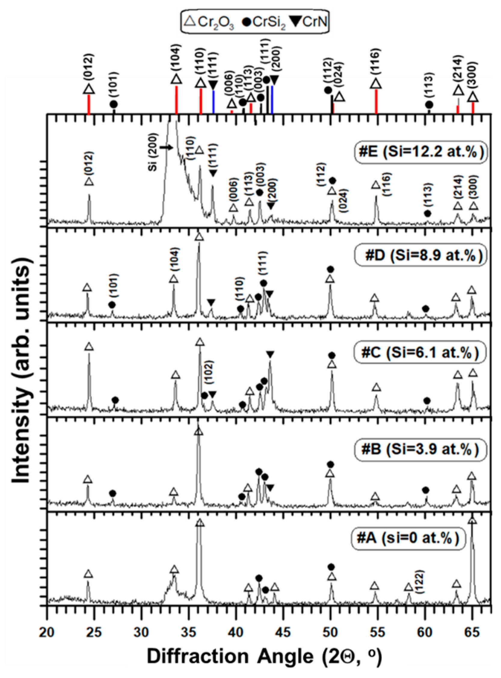
The X-ray diffraction patterns of five as-deposited thin films are shown in Figure 1. The standard diffraction peaks of CrN (JCPDS card # 11-0065), β-Cr2N (JCPDS card # 35-0803), and Cr (JCPDS card # 06-0694) are also indicated in Figure 1.
A mixture of CrN and β-Cr2N phases can be seen for the #A, #B, #C and #D films, whereas the diffraction peak corresponding to Cr or Cr-Si interlayer is also observed. However, a small hump in the range from 39° to 47° diffraction angles indicates an amorphous-like X-ray diffraction pattern for #E film containing 12.2 at.% Si. No XRD peaks corresponding to Si3N4 and CrSi2 are found in Figure 1. The CrN (111) and (200) diffraction peaks shift around 0.8°–1.2° to a higher diffraction angle in the Cr-Si-N films due to the solid solution effect of Si atoms into CrN lattice, which was reported elsewhere [10]. The existence of Cr2N and CrN mixed phases can be attributed to the under-stoichiometric N/(Cr + Si) ratios of 0.69 to 0.62 for the #A (CrNx) and #B–#D (Cr-Si-N) films as listed in Table 2. Meanwhile, the effect of Si atom acting as a substitutional solid solution element in the CrN lattice and expelling extra Cr ions to reacting with the Cr–N phase to form Cr2N [21,24] is also a possible reason.
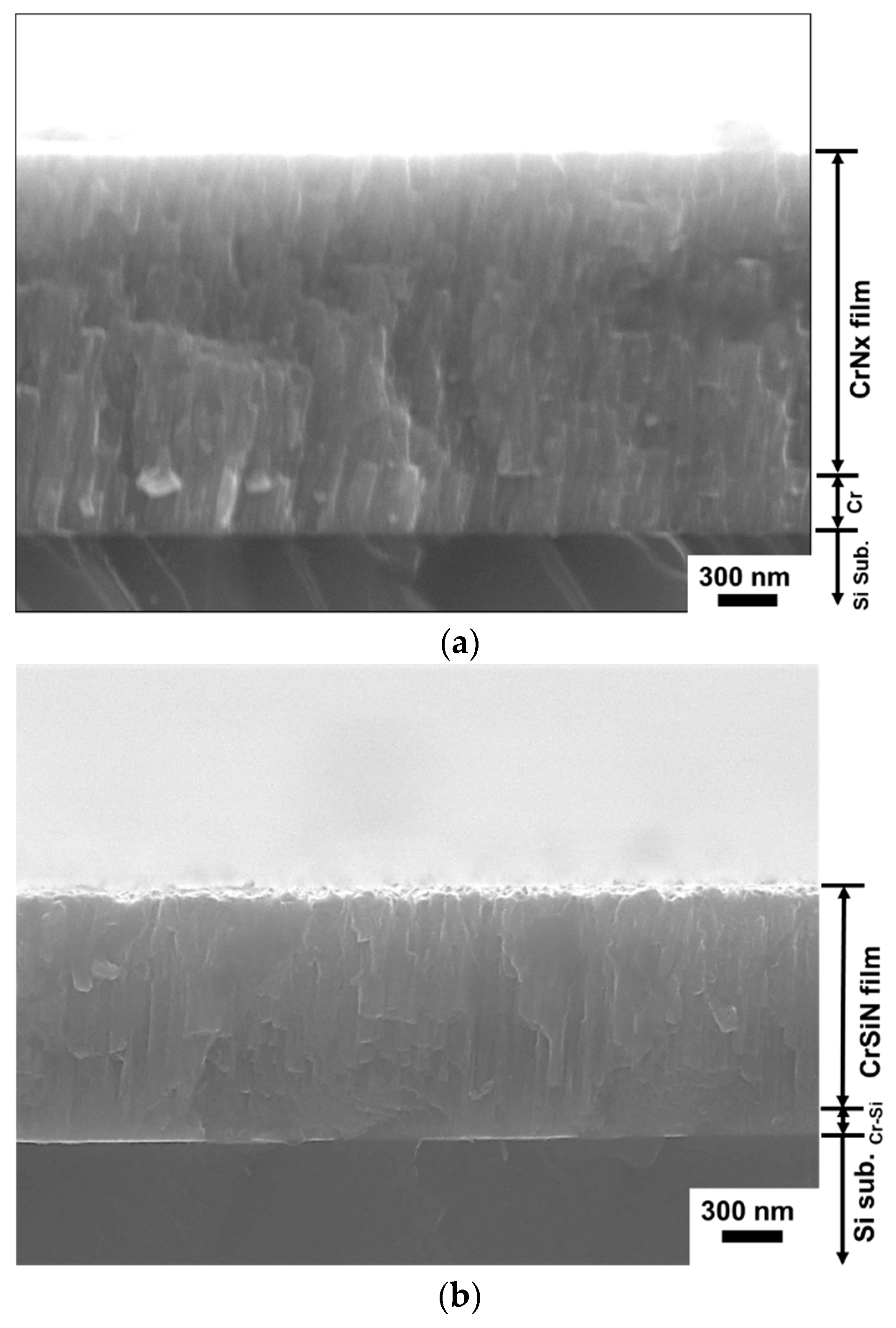
Through SEM analysis of cross-sectional microstructure of the #A thin film, as illustrated in Figure 2a, a typical coarse columnar structure of CrNx film and a 270 nm thick pure Cr interlayer can be seen. The width of columnar structure decreases with increasing Si content, which can be found for the #B, #C and #D films as shown in Figure 2b–d. On the other hand, a featureless, dense, and compact morphology is observed for the #E film containing 12.2 at.% Si in Figure 2e. The thickness of Cr-Si interlayer for each Cr-Si-N film is around 150 nm. Although the exact chemical composition of each Cr-Si layer was not measured, the microstructure of Cr-Si interlayer becomes dense and featureless, and the boundary line between the Cr-Si interlayer and Cr-Si-N film becomes ambiguous as the silicon content of Cr-Si interlayer increases, which can be seen in Figure 2b–e. The average thickness of each thin film is measured and listed in Table 2.
The highest thickness of 1.9 μm is obtained for the #A film due to its higher Cr target power of 500 W. In general, the Cr-Si-N film thickness increases with increasing Si content due to its higher Si target power during the sputtering process. For example, the thickness values for the #B and #E films increase from 1.23 to 1.56 μm as the Si target power and Si content increase from 65 to 224 W and from 3.9 to 12.2 at.%, respectively.
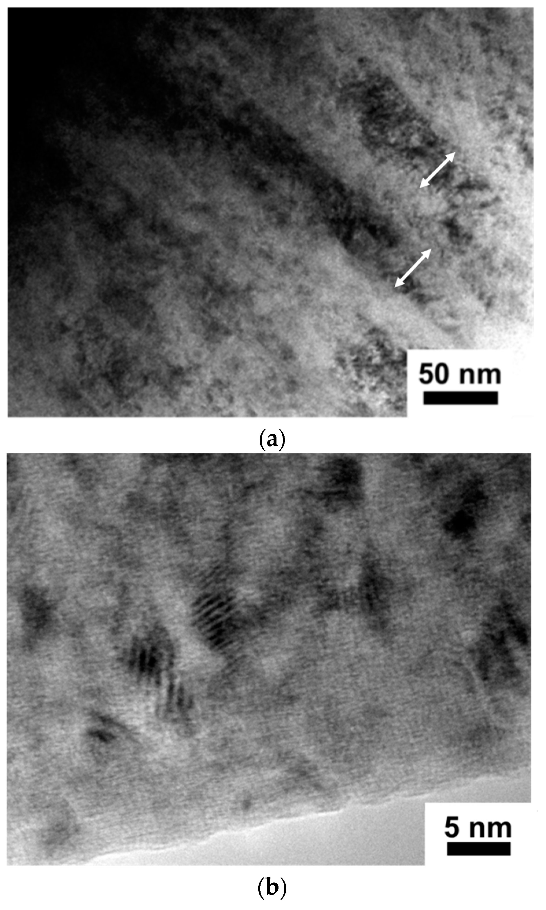
The cross-sectional images at higher magnification of the #B and #E films was analyzed by TEM, as depicted in Figure 3a,b. It is obvious that a dense columnar microstructure, around several tens of nanometer wide as indicated by white arrows, can be found for the #B film in Figure 3a. Meanwhile, a nanocomposite microstructure containing CrN/Cr2N nanograins, around several nanometer in diameter, embedded in a SiNx amorphous matrix is clearly seen in Figure 3b. The grain size refinement of Cr-Si-N film brought by the formation of the amorphous SiNx phase is confirmed in this work, which is also reported elsewhere [22,24,25]. This nanocomposite microstructure is responsible for the amorphous-like XRD pattern of the #E film in Figure 1 and the glassy cross-sectional morphology as depicted in Figure 2e. The average surface roughness, Ra, of each thin film is listed in Table 2. The lowest average surface roughness of 1.4 nm can be seen on the #E thin film, possibly due to its SiNx amorphous matrix. Meanwhile, the highest average surface roughness of 9.1 nm is observed for the #D film, which may be caused by the instability of substrate bias voltage during deposition.
3.2. Oxidation Kinetics of Thin Films at 1000 °C
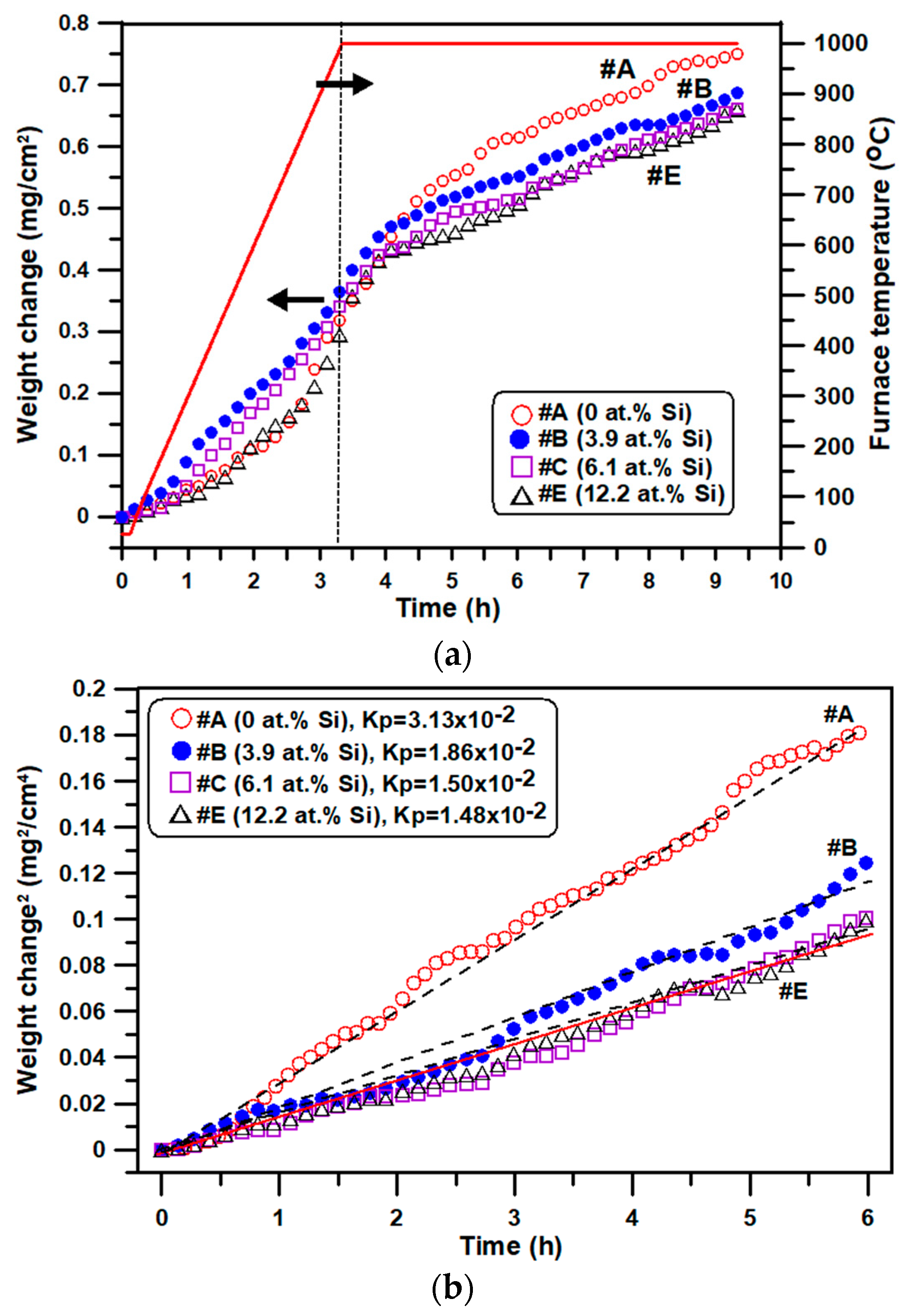
The weight gain plots of all thin films, except #D, heating from room temperature to 1000 °C and holding for 6 h are illustrated in Figure 4a. The furnace temperature versus the heating time is also indicated by a red line. The heating time from room temperature to 1000 °C was around 3.3 h and the isothermal time at 1000 °C was 6 h. The continuous heating and isothermal heating regions are divided by a dashed line in Figure 4a. The weight gain for each film during dynamic heating from room temperature to 1000 °C was set to zero. The weight gain of each thin film at the isothermal heating at 1000 °C for 6 h was measured again. It is important to point out that these coatings were significantly oxidized, and the weight gains were ranging from 0.31 to 0.37 mg/cm2 before reaching 1000 °C due to a very low heating rate of 5 °C/min in air.
The relationships between the square of weight gain values versus isothermal oxidation time at 1000 °C are shown in Figure 4b. In addition, dashed fitting lines and the calculated parabolic rate constants (unit: mg2/cm4/h) of four thin films are depicted in Figure 4b.
During the heating from room temperature to 1000 °C, the #B film had the highest weight gain as compared with other thin films. On the other hand, the lowest weight gain values can be seen for the #A and #E films during the first stage of heating. We suggest that the #A film can easily form the Cr2O3 oxide layer on the surface for providing initial oxidation protection. After the furnace temperature was heated to 1000 °C and kept for 6 h, a rapid increase of weight gain to the highest value of 0.75 mg/cm2 can be found for the #A film. Although the weight gain data at 1000 °C for the first hour of four thin films are very close, as shown in Figure 4b, we can still recognize that the highest weight gain can be seen for the #A film, whereas the second highest weight gain can be found for #B film. Meanwhile, the weight gain values of #E and #C are lower and very close to each other. It is also noticed that the weight gains of the #B, #C and #E thin films are higher during dynamic heating from room temperature to 1000 °C than these during isothermal heating at 1000 °C, because of the formation of protective oxide layers during dynamic heating, which provide further oxidation resistance and less weight gain for these Si-containing films during isothermal heating at 1000 °C.
The #D film is not shown in Figure 4 due to a severe mass loss that occurred during the heating period of the oxidation test, indicating a severe delamination of thin film. We found that a very large portion of the #D film spalled away and exhibited very poor adhesion properties on silicon substrate during heating. According to the observation of the residual stress values measured on the as-deposited thin films, as listed in Table 2, it appears that only the #D film exhibited a tensile stress of 0.24 GPa, whereas the other films were in compressive stress states. It is reported [26] that the total stress of an as-deposited CrN thin film is the sum of the contributions by thermal expansion, ion peening, and grain boundaries. Tensile stress is generated at grain boundaries during cooling from high deposition temperature to room temperature, whereas compressive stress is produced by ion peening [26]. Unlike the other thin films, the ion peening effect of the #D film was not pronounced, which may have been caused by the instability of substrate bias voltage during deposition. We suggest that the compressive residual stress of thin film can compensate for the thermal stress induced from the mismatch of thermal expansion coefficients, α, between Si substrate (αSi = 2.6 × 10⁻⁶ K−1 [26]) and CrN film (αCrN = 7.16 × 10⁻⁶ K−1 [26]) during heating and cooling. On the other hand, it appears that tensile residual stress incorporated with the thermal stress peels off the thin film easily during heating.
The parabolic-like oxidation weight gain curves in Figure 4a indicate diffusion-controlled reactions prevailed during oxidation at 1000 °C. Both the weight gains and parabolic rate constants decrease gradually with increasing Si content of Cr-Si-N thin films. It can be found that the weight gain, 0.428 mg/cm2, and parabolic rate constant, 3.13 × 10⁻² mg2/cm4/h, are the highest for the #A CrNx thin film, whereas the lowest values of 0.317 mg/cm2 and 1.48 × 10⁻² mg2/cm4/h, are found for the #E film containing the highest Si content of 12.2 at.%. Apparently, high temperature oxidation resistance enhanced by the addition of Si to the CrN thin films was obtained in this study. Furthermore, the weight gain and Kp values of the #C and #E films are almost the same, which indicates the Cr-Si-N thin films containing more than 6.1 at.% Si have similar oxidation kinetics at 1000 °C for 6 h. The parabolic oxidation behavior of CrN film at 700–900 °C and at 760–1160 °C were reported by Lin et al. [4] and Meng and coworkers [3], respectively. A Kp value around 2.73 × 10⁻² mg2/cm4/h was calculated for the CrN film oxidized at 960 °C for 1 h [3], which is around 13% less than that of the #A film at 1000 °C. Kim and coworkers [9] also reported the oxidation kinetics of CrN, Cr0.78Si0.22N, and Cr0.67Si0.33N films at 800–1000 °C in air. The parabolic rate constant of Cr0.78Si0.22N film at 1000 °C is calculated around 4.46 × 10⁻² mg2/cm4/h, whereas a much higher value of 3.16 × 10⁻¹ mg2/cm4/h is calculated for the CrN film [9]. Nevertheless, the Kp of CrN or Cr-Si-N film at high temperature oxidation can be varied due to the difference of microstructure, chemical composition, and defect densities of thin films. It is important to point out that the Kp value decreases with increasing Si content of Cr-Si-N film, as shown in Figure 4b, which can provide very solid evidence for the oxidation resistance improvement by the addition of higher Si concentration in this study.
3.3. Phase and Microstructure of Thin Films after Oxidation Test at 1000 °C
The X-ray diffraction patterns of oxidized thin films are shown in Figure 5. Since the #D film was severely delaminated during the oxidation test, the XRD analysis of the #D film was conducted using the delaminated film from the crucible.
The phases of #A are composed of Cr2O3 (JCPDS card # 38-1479) and CrSi2 (JCPDS card # 35-0781). No CrN phase can be observed due to its full oxidation into the chromium oxide phase. Strong Cr2O3 diffraction peaks and some CrSi2 peaks are found for the #B film as well. However, a very weak CrN (200) peak is shown around 43.7° for the #B film. For the #C, #D, and #E films, it is obvious that the primary peak is still the Cr2O3 (110), whereas the CrN phase can be clearly identified by the (111) peak at 37.5° and the (200) peak at 43.7°. A rather high intensity of the CrN (111) peak shown for the #E thin film indicates a higher amount of the CrN phase left after the oxidation test. In general, the CrSi2 phase is observed in all five thin films, but no Cr3Si phase is recognized, which was reported by Castaldi et al. [10], in the Cr-Si-N coating oxidized at 1000 °C for 40 min. We suggest that the CrSi2 phase observed in each thin film came from the interactions between CrN/Cr-Si-N film, Cr-Si interlayer, and Si substrate at high temperature for 6 h. However, the crystalline SiO2 phase, which has been reported elsewhere [8,9,10], is not found in this work. Based on the Gibb’s free energy calculation for the oxidation of the Cr2N and CrN phases at 1000 °C, the reaction is favorable for the oxidation of the Cr2N phase [27]. According to the fact that the Cr2N phase is absent, and only the CrN phase can be recognized in the XRD results in Figure 5 for four Si-containing films after oxidation at 1000 °C, we therefore suggest that this phase evolution is possibly due to the preferential oxidation of the Cr2N phase and an increased depletion of Cr element of the Cr2N phase.
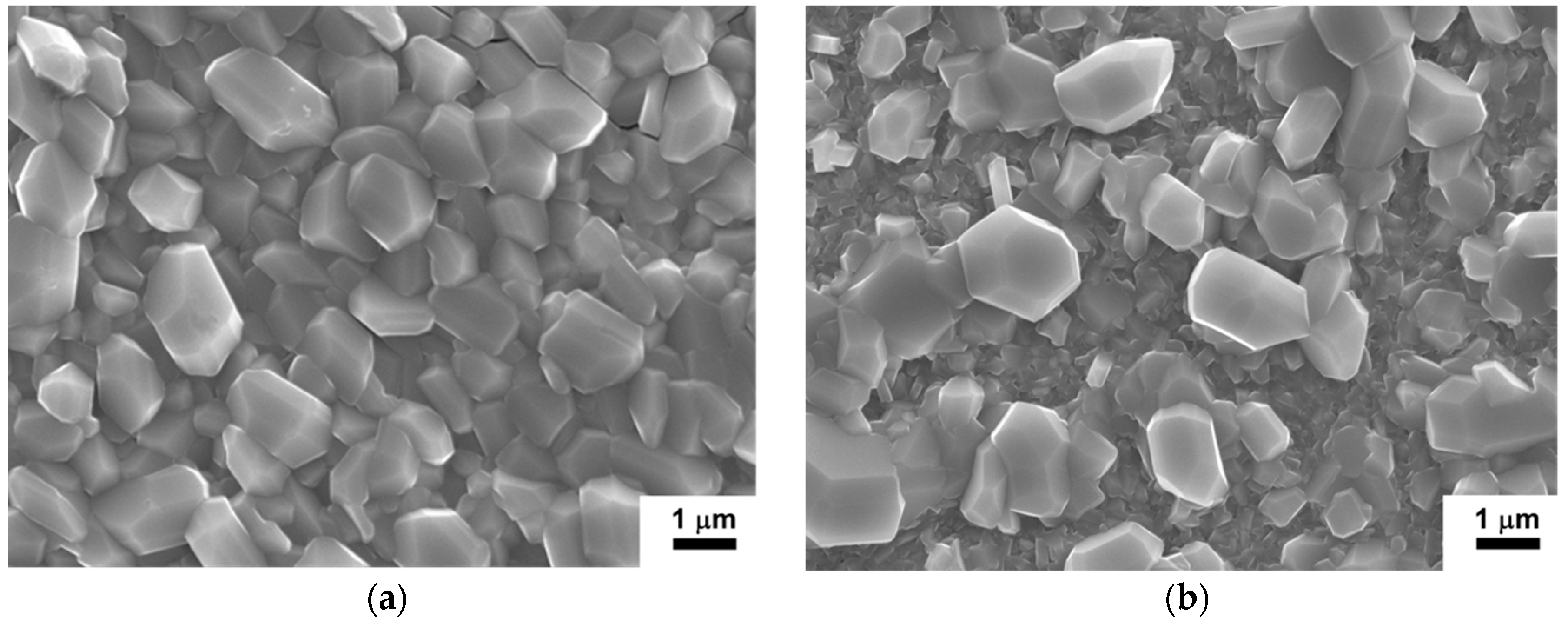
The surface morphology of the oxidized #A thin film, as shown in Figure 6a, exhibits large faceted grains, which can be confirmed as Cr2O3 by FE-EPMA analysis and XRD results. The grain size of Cr2O3 is around 1–3 μm in diameter. On the other hand, the surface morphology of the oxidized #E film is shown in Figure 6b. The number of faceted Cr2O3 grains decreases as Si content increases to 12.2 at.%. A very dense Si-containing oxide layer with a smaller grain size can be found under the faceted grains. Apparently, the dense Si-containing oxide layer beneath the large surface Cr2O3 grains becomes a protective layer to the thin film. It was reported that Cr oxidizes faster than Si due to the strong covalent bonding of amorphous silicon nitride, which restricts the outward diffusion of Si [10]. After the oxidation of Cr, the amorphous SiNx phase and Si atoms dissolved in CrN structures start to oxidize into amorphous silicon oxide, which can impinge both outward and inward diffusion paths of other elements [8].
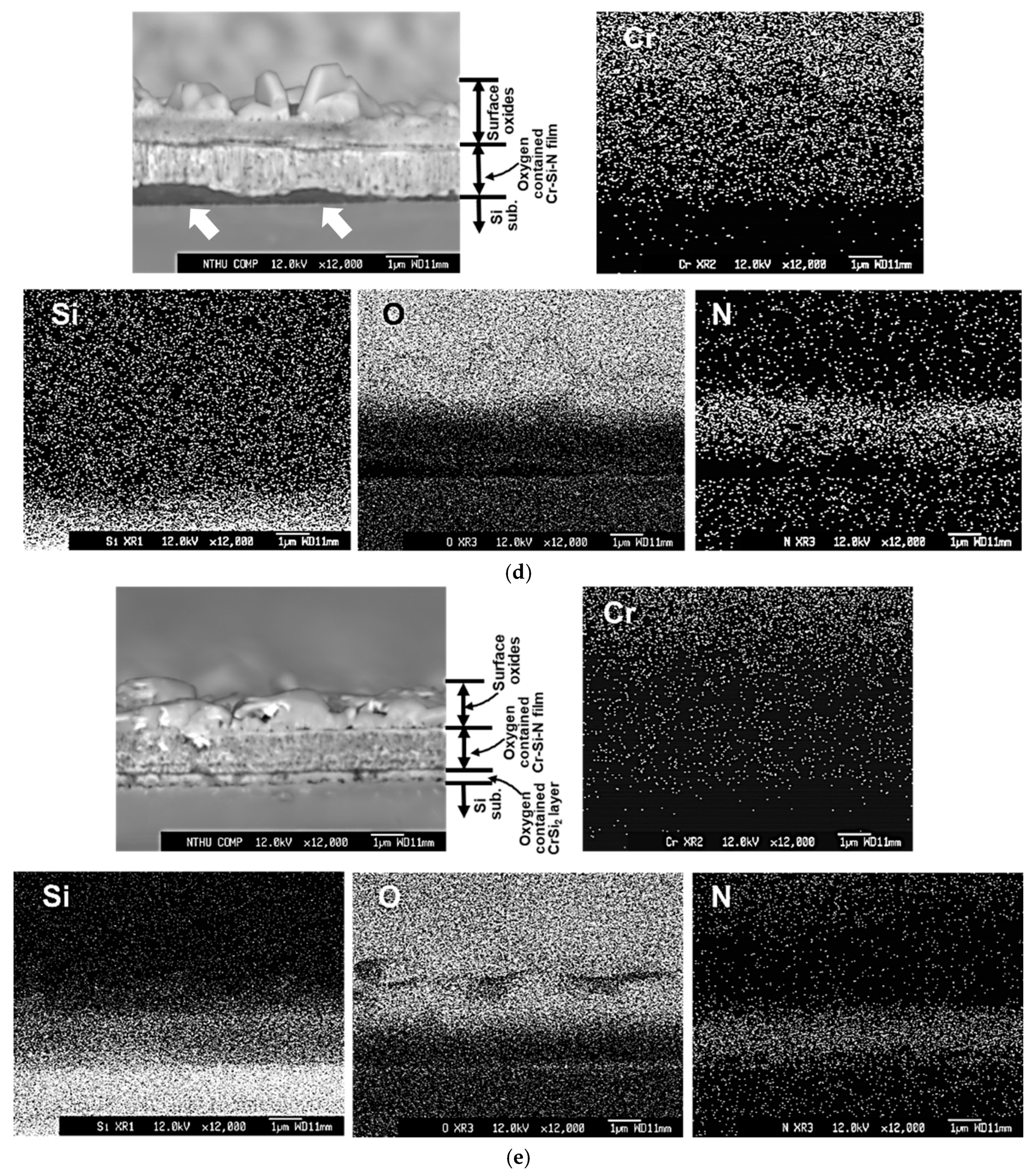
Figure 7 depicts the cross-sectional backscattered electron images and X-ray mappings of Cr, O, Si, and N elements by FE-EPMA of all thin films after the oxidation test. Since the #D film was almost delaminated after the oxidation test, the cross-sectional image of #D was taken from the retained film, which was still adhered on the Si substrate. The outermost oxide layer, remaining oxygen-containing Cr-Si-N nitride layer, oxygen-containing CrSi2 region, and Si substrate are indicated for each film in Figure 7. In Figure 7a, the whole CrNx film was almost totally oxidized, which can be confirmed by the X-ray mapping of O. It is obvious that a dense Cr2O3 oxide layer around 2.6 μm thick is formed on the outermost surface region, whereas a porous oxide zone around 1.5 μm in thickness is measured between the Cr2O3 surface layer and the inner granular structured oxygen-containing CrSi2 region, as shown in Figure 7a. This porous structure is full of voids, which were possibly formed due to the rapid outward diffusion of Cr and N atoms and inward diffusion of O atoms during high temperature oxidation. Lin and coworkers [4] also discovered a similar porous microstructure in the CrN film after oxidation at 1000 °C for 1 h in air. The phase transformation of Cr2N to CrN during high temperature oxidation is also attributed to the formation of voids [27]. According to the X-ray mappings of N and O, very small amounts of nitrogen and oxygen concentrations can be seen in the upper and lower region of the CrSi2 layer. Since the melting point of Si is around 1440 °C, the diffusion reaction of Si plays an important role in the formation of the CrSi2 phase during oxidation at 1000 °C. Therefore, the original thin Cr interlayer was further reacted with Si substrate and became a granular oxygen- and nitrogen-containing CrSi2 region because of the poor oxidation resistance of CrNx film.
In Figure 7a, the thickness of the porous nitrogen- and oxygen-containing CrSi2 region is around 1.6 μm, possibly due to the severe interdiffusion of Si, N and O elements in this region at high temperature. This CrSi2 region is also full of voids, which also make the layer thickness become thicker. For the #B films, as shown in Figure 7b, faceted Cr2O3 grains can be found on the surface oxide layer, which is around 2.4 μm thick. A complex porous morphology is observed in the oxygen- and nitrogen-containing CrSi2 phase region with a thickness around 1.5 μm. Some voids, oxides, and needle-like CrSi2 phases penetrating the Si substrate indicate that complex reactions occurred between the original thin Cr-Si interlayer and Si substrate during 1000 °C heating. Based on the X-ray mapping of N, the oxygen-containing Cr-Si-N film becomes discontinuous and porous. The estimated thickness of this porous Cr-Si-N layer is around 1.0 μm, as depicted in Figure 7b. On the other hand, layered microstructures are observed for the #C, #D, and #E films, as illustrated in Figure 7c–e. According to the backscattered electron image (BEI) micrographs and the corresponding X-ray mappings of N, the remaining thickness values of the oxygen-containing Cr-Si-N layer for the #C, #D, and #E films are around 0.9, 1.4 and 1.3 μm, respectively. The remaining oxygen-containing Cr-Si-N layer of the #C film shows a columnar microstructure. As compared with the oxygen-containing Cr-Si-N structures in Figure 7c–e, a more compact microstructure can be found for the #D and #E films. For the #C and #E films, the thickness values of the porous oxygen-containing CrSi2 phase regions are around 0.9 and 0.27 μm thick, respectively. However, almost no CrSi2 phase region can be found for the #D film, possibly due to the delamination of thin film from the Si substrate, as indicated by the arrows in Figure 7d. Besides, a very small amount of oxygen content can be seen in the CrSi2 phase region in Figure 7e, implying a good oxidation resistance of the #E film at 1000 °C. The thicknesses of the CrSi2 phase regions for the #A, #B, #C and #E films are different as the oxidation resistance of these thin films are different. A better oxidation resistance of Cr-Si-N thin film can decrease the inward/outward diffusion reactions of O and Si, and lowers the amount of voids and reduces the thickness of such CrSi2 phase regions. Although the parabolic rate constant values of the #C and #E films are very close, we can still confirm that a better oxidation resistance can be seen for the #E film due to its dense microstructure, thicker remaining Cr-Si-N layer (around 1.3 μm), and a thin and relatively low oxygen-containing CrSi2 interlayer (around 0.27 μm in thickness) after the oxidation test.
We believe that the amorphous silicon nitride matrix of the nanocomposite microstructure of the #E film plays an important role for effectively blocking the outward and inward diffusion of Cr, N, Si and O elements during high temperature oxidation. It is also important to point out that a continuous Si-rich oxide layer can be observed between the surface oxide layer and the the #E Cr-Si-N film layer, as depicted in Figure 7e. This microstructure provides solid evidence for its good oxidation resistance at 1000 °C for 6 h. There are two factors that can affect the performance of the CrNx and Cr-Si-N thin films during high temperature oxidation testing; one is the residual stress state in the as-deposited film, and the other is the Si content of Cr-Si-N film. Apparently, increasing the amount of Si content, for example, higher than 8.9 at.%, enhances the high temperature oxidation resistance of Cr-Si-N thin film. However, the residual tensile stress, such as the #D film in this study, shows a detrimental effect on the adhesion properties of thin film and thus eliminates the advantage of high Si content for oxidation resistance improvement.
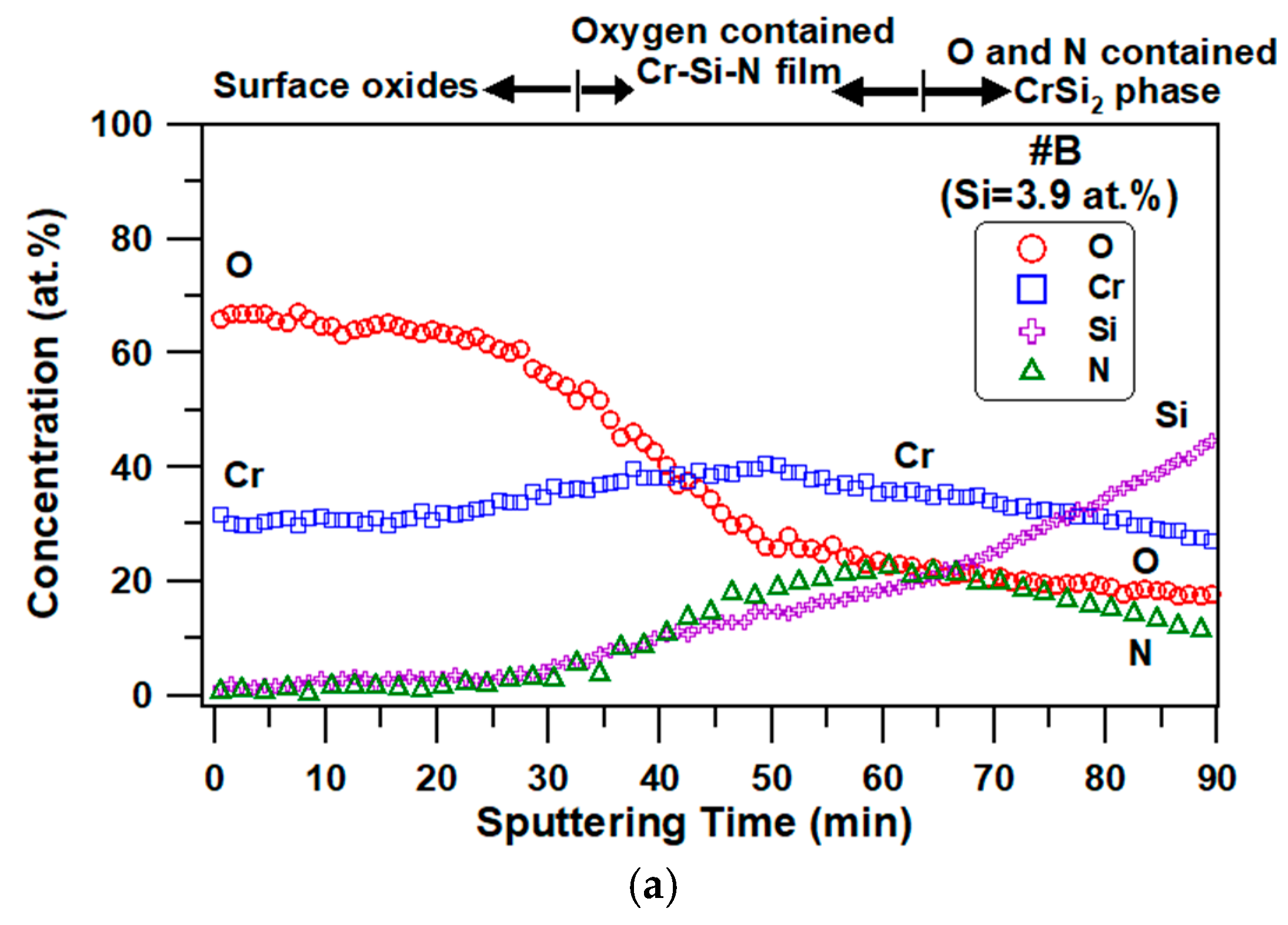
The AES depth profiles of the oxidized #B and #E films are depicted in Figure 8a,b, respectively. Estimated structure evolutions of thin films are also drawn based on the concentration profiles and XRD results in Figure 5. For the #B film, it is obvious that an inward diffusion of oxygen is shown, while the outward diffusions of Cr, N, and Si are revealed. A thick Cr2O3 oxide region is formed on the surface based on the chemical composition analysis data shown in Figure 8a, which is also consistent with the microstructure observation and the X-ray mapping of O element in Figure 7b.
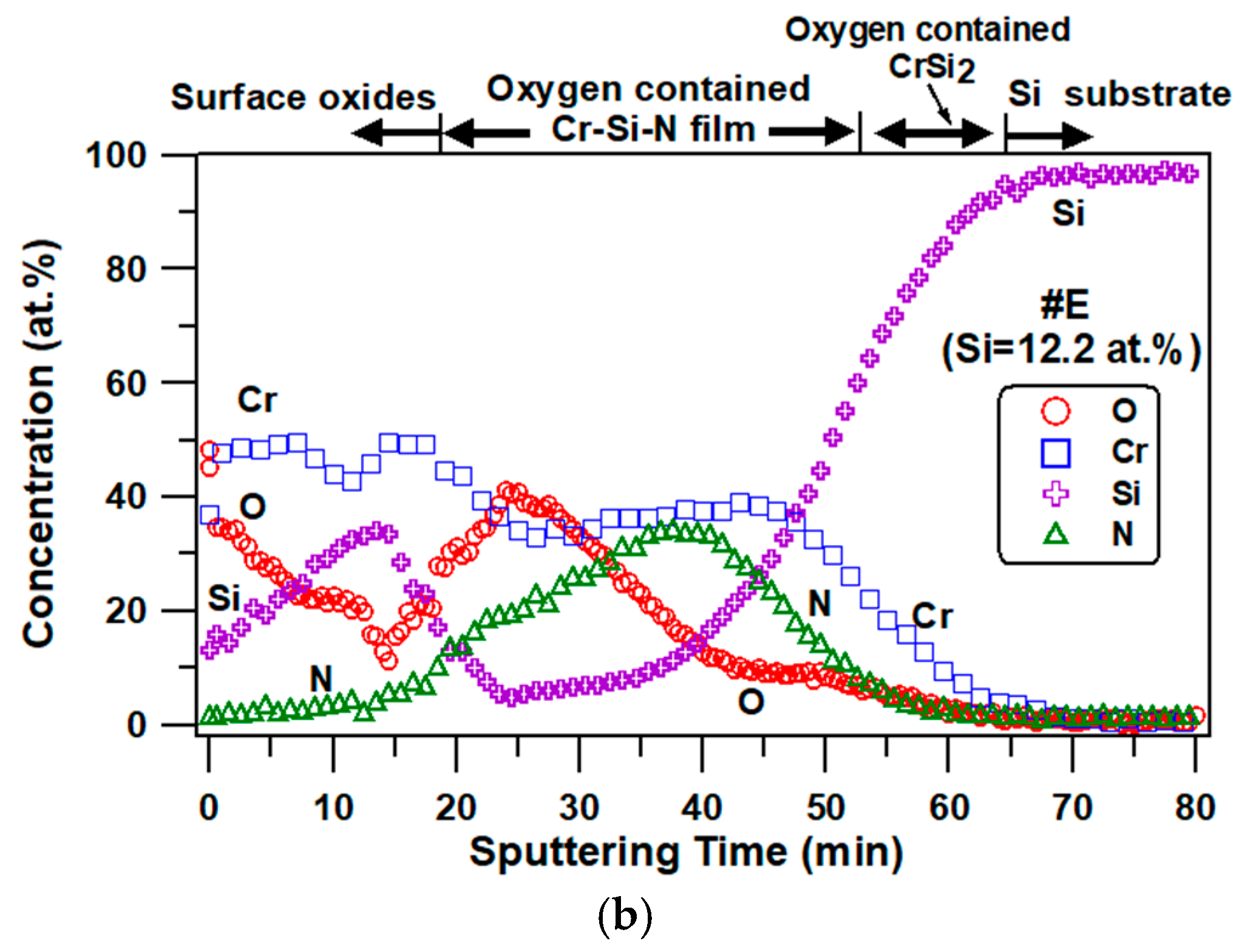
Based on the O and N profiles, the oxygen content reaches 24 at.% in the Cr-Si-N film of #B. The higher Si concentration, around 10–20 at.%, in the thin film is attributed to the outward diffusion of Si atoms from the 150-nm-thick Cr-Si interlayer and Si substrate. It is important to point out that the AES depth profile of the oxidized #B film does not reach the Si substrate after sputter etching for 90 min due to its extremely large thickness, around 4.9 μm, as illustrated in the BEI micrograph in Figure 7b. Figure 8b illustrates the AES depth profiles of the #E film, where a rather complex concentration profiling of elements is observed as compared with that of the #B film. The Si substrate and the CrSi2 layer are recognized in Figure 8b. The outer surface is rich in Cr and O, and is depleted in N, indicating an oxide layer containing around 12 at.% Si was formed, which corresponds to the dense surface oxide layer as shown in Figure 7e. The average chemical composition of the outermost oxide region is 38.7% Cr, 46.8% O, 12.8% Si and 1.7% N (in at.%), which deviates from the chemical composition of Cr2O3 oxide. We suggest that this chemical deviation can be attributed to the partial spallation of the outermost Si-containing Cr2O3 oxide layer. In addition, the higher surface roughness brought by the large crystallites on the oxidized surface can affect the accuracy of chemical analysis of AES. A silicon concentration pile-up layer, reaching around 35 at.%, is discovered in the region between the surface oxide and CrSiN film, indicating a high Si-containing amorphous silicon oxide layer, which can retard the diffusion paths of O, Cr, and N. A similar finding of the Si and O-rich layer can be observed in the X-ray mappings of Si and O in Figure 7e. The N content in the Cr-Si-N film ranges from 15 to 34 at.%, which is lower than that before oxidation. On the other hand, the Si content varies from 6 to 42 at.% in the Cr-Si-N film, which is attributed to the outward diffusion of Si from the Cr-Si interlayer and Si substrate. The O content decreases gradually from 40 to 8 at.% in the Cr-Si-N film. In the literature, the oxidation resistance of CrSiN [8,9,10,11], CrAlN, and CrAlSiN films [17,19,20] at high temperature were greatly improved by the adequate amount of Si added. The improvement mechanism by the formation of an amorphous silicon oxide layer is also valid in this study. Finally, we can conclude that the higher Si-containing Cr-Si-N film enhanced its oxidation resistance due to the formation of dense surface Cr2O3 layer and the amorphous silicon oxide layer for retarding the outward and inward diffusion reactions at 1000 °C. Even a very similar parabolic rate constant was obtained for the #C and #E films; the best oxidation resistance of the #E film containing 12.2 at.% Si can be confirmed by its dense microstructure in Figure 7e and the AES analysis in Figure 8b.
4. Conclusions
One CrNx and four Cr-Si-N thin films with Si contents ranging from 3.9 to 12.2 at.% were fabricated by a pulsed DC magnetron sputtering system. Mixed CrN and Cr2N phases were formed on the CrNx and Cr-Si-N thin films containing up to 8.9 at.% Si. A nanocomposite microstructure consisting of CrN/Cr2N nanograins embedded in the amorphous silicon nitride matrix was observed for the Cr-Si-N thin film with 12.2 at.% Si content. The oxidation resistance of CrNx thin films at 1000 °C for 6 h was greatly improved by the addition of at least 8.9 at.% Si. The weight gains and parabolic rate constants decreased with increasing Si content in the Cr-Si-N film. A thicker Cr-Si-N layer of around 1.3 μm in thickness, the lowest parabolic rate constant of 1.48 × 10⁻² mg2/cm4/h, and the lowest weight gain of 0.317 mg/cm2 were observed for Cr-Si-N film containing 12.2 at.% Si after the isothermal oxidation test at 1000 °C for 6 h. According to the oxidation kinetics, XRD, cross-sectional microstructures, X-ray mapping, and depth profiling analysis, we can conclude that Cr-Si-N film with more than 8.9 at.% Si concentration can provide sufficient oxidation resistance at 1000 °C for 6 h in ambient air. The best oxidation resistance of Cr-Si-N film at 1000 °C was obtained when the Si content reached 12.2 at.%. It is noticeable that the tensile residual stress state of the as-deposited thin film should be avoided, which is responsible for the thin film delamination during high temperature oxidation testing.
Author Contributions
Writing—Original Draft Preparation, B.-S.L.; Methodology, Y.-C.C.; Supervision, J.-W.L.; Writing—Review and Editing, J.-W.L.; Funding Acquisition, B.-S.L. and J.-W.L.
Funding
This research was funded by the Ministry of Science and Technology (MOST), Taiwan (Nos. 106-2218-E-131-003, 107-2218-E-131-001, 107-2221-E-131-002-MY3 and 108-2218-E-182-030) and the Chang Gung Memorial Hospital (Nos. CMRPD5H0032 and BMRP280).
Conflicts of Interest
The authors declare no conflict of interest.
References
- Lee, J.W.; Kuo, Y.C.; Wang, C.J.; Chang, L.C.; Liu, K.T. Effects of substrate bias frequencies on the characteristics of chromium nitride coatings deposited by pulsed DC reactive magnetron sputtering. Surf. Coat. Technol. 2008, 203, 721–725. [Google Scholar] [CrossRef]
- Dinu, M.; Mouele, E.; Parau, A.; Vladescu, A.; Petrik, L.; Braic, M. Enhancement of the corrosion resistance of 304 stainless steel by Cr–N and Cr(N,O) coatings. Coatings 2018, 8, 132. [Google Scholar] [CrossRef]
- Meng, C.; Yang, L.; Wu, Y.; Tan, J.; Dang, W.; He, X.; Ma, X. Study of the oxidation behavior of CrN coating on Zr alloy in air. J. Nucl. Mater. 2019, 515, 354–369. [Google Scholar] [CrossRef]
- Lin, J.; Zhang, N.; Sproul, W.D.; Moore, J.J. A comparison of the oxidation behavior of CrN films deposited using continuous dc, pulsed dc and modulated pulsed power magnetron sputtering. Surf. Coat. Technol. 2012, 206, 3283–3290. [Google Scholar] [CrossRef]
- Navinšek, B.; Panjan, P.; Milošev, I. Industrial applications of CrN (PVD) coatings, deposited at high and low temperatures. Surf. Coat. Technol. 1997, 97, 182–191. [Google Scholar] [CrossRef]
- Khamseh, S.; Araghi, H. A study of the oxidation behavior of CrN and CrZrN ceramic thin films prepared in a magnetron sputtering system. Ceram. Int. 2016, 42, 9988–9994. [Google Scholar] [CrossRef] [Green Version]
- Ding, J.; Zhang, T.; Yun, J.M.; Kang, M.C.; Wang, Q.; Kim, K.H. Microstructure, mechanical, oxidation and corrosion properties of the Cr-Al-Si-N coatings deposited by a hybrid sputtering system. Coatings 2017, 7, 119. [Google Scholar] [CrossRef]
- Thobor-Keck, A.; Lapostolle, F.; Dehlinger, A.S.; Pilloud, D.; Pierson, J.F.; Coddet, C. Influence of silicon addition on the oxidation resistance of CrN coatings. Surf. Coat. Technol. 2005, 200, 264–268. [Google Scholar] [CrossRef]
- Kim, J.W.; Kim, K.H.; Lee, D.B.; Moore, J.J. Study on high-temperature oxidation behaviors of Cr–Si–N films. Surf. Coat. Technol. 2006, 200, 6702–6705. [Google Scholar] [CrossRef]
- Castaldi, L.; Kurapov, D.; Reiter, A.; Shklover, V.; Schwaller, P.; Patscheider, J. High temperature phase changes and oxidation behavior of Cr–Si–N coatings. Surf. Coat. Technol. 2007, 202, 781–785. [Google Scholar] [CrossRef]
- Mège-Revil, A.; Steyer, P.; Fontaine, J.; Pierson, J.F.; Esnouf, C. Oxidation and tribo-oxidation of nanocomposite Cr–Si–N coatings deposited by a hybrid arc/magnetron process. Surf. Coat. Technol. 2009, 204, 973–977. [Google Scholar] [CrossRef]
- Lackner, J.; Waldhauser, W.; Major, L.; Kot, M. Tribology and micromechanics of chromium nitride based multilayer coatings on soft and hard substrates. Coatings 2014, 4, 121–138. [Google Scholar] [CrossRef]
- Azizpour, A.; Hahn, R.; Klimashin, F.F.; Wojcik, T.; Poursaeidi, E.; Mayrhofer, P. Deformation and cracking mechanism in CrN/TiN multilayer coatings. Coatings 2019, 9, 363. [Google Scholar] [CrossRef]
- Tien, S.K.; Duh, J.G.; Lee, J.W. Oxidation behavior of sputtered CrN/AlN multilayer coatings during heat treatment. Surf. Coat. Technol. 2007, 201, 5138–5142. [Google Scholar] [CrossRef]
- Tytko, D.; Choi, P.P.; Raabe, D. Oxidation behavior of AlN/CrN multilayered hard coatings. Nano Converg. 2017, 4, 15. [Google Scholar] [CrossRef]
- Männling, H.D.; Atil, D.S.; Moto, K.; Jilek, M.; Veprek, S. Thermal stability of superhard nanocomposite coatings consisting of immiscible nitrides. Surf. Coat. Technol. 2001, 146–147, 263–267. [Google Scholar] [CrossRef]
- Chen, H.W.; Chan, Y.C.; Lee, J.W.; Duh, J.G. Oxidation resistance of nanocomposite CrAlSiN under long-time heat treatment. Surf. Coat. Technol. 2011, 206, 1571–1576. [Google Scholar] [CrossRef]
- Chang, C.C.; Chen, H.W.; Lee, J.W.; Duh, J.G. Influence of Si contents on tribological characteristics of CrAlSiN nanocomposite coatings. Thin Solid Films 2015, 584, 46–51. [Google Scholar] [CrossRef]
- Chang, C.C.; Chen, H.W.; Lee, J.W.; Duh, J.G. Development of Si-modified CrAlSiN nanocomposite coating for anti-wear application in extreme environment. Surf. Coat. Technol. 2015, 284, 273–280. [Google Scholar] [CrossRef]
- Chen, H.W.; Chan, Y.C.; Lee, J.W.; Duh, J.G. Oxidation behavior of Si-doped nanocomposite CrAlSiN coatings. Surf. Coat. Technol. 2010, 205, 1189–1194. [Google Scholar] [CrossRef]
- Lee, J.W.; Chang, Y.C. A study on the microstructures and mechanical properties of pulsed DC reactive magnetron sputtered Cr–Si–N nanocomposite coatings. Surf. Coat. Technol. 2007, 202, 831–836. [Google Scholar] [CrossRef]
- Lin, H.H.; Chou, C.C.; Lee, J.W. Tribological properties of Cr–Si–N nanocomposite film adherent silicon under various environments. Thin Solid Films 2010, 518, 7509–7514. [Google Scholar] [CrossRef]
- Stoney, G.G. The tension of metallic films deposited by electrolysis. Proc. R. Soc. Lond. Ser. A 1909, 82, 172–175. [Google Scholar] [CrossRef] [Green Version]
- Lee, H.Y.; Jung, W.S.; Han, J.G.; Seo, S.M.; Kim, J.H.; Bae, Y.H. The synthesis of CrSiN film deposited using magnetron sputtering system. Surf. Coat. Technol. 2005, 200, 1026–1030. [Google Scholar] [CrossRef]
- Sandu, C.S.; Sanjinés, R.; Benkahoul, M.; Medjani, F.; Lévy, F. Formation of composite ternary nitride thin films by magnetron sputtering co-deposition. Surf. Coat. Technol. 2006, 201, 4083–4089. [Google Scholar] [CrossRef]
- Janssen, G.C.A.M.; Tichelaar, F.D.; Visser, C.C.G. Stress gradients in CrN coatings. J. Appl. Phys. 2006, 100, 093512. [Google Scholar] [CrossRef] [Green Version]
- Qi, Z.B.; Liu, B.; Wu, Z.T.; Zhu, F.P.; Wang, Z.C.; Wu, C.H. A comparative study of the oxidation behavior of Cr2N and CrN coatings. Thin Solid Films 2013, 544, 515–520. [Google Scholar] [CrossRef]
Figure 1.
The X-ray diffraction patterns of as-deposited CrNx and Cr-Si-N thin films.
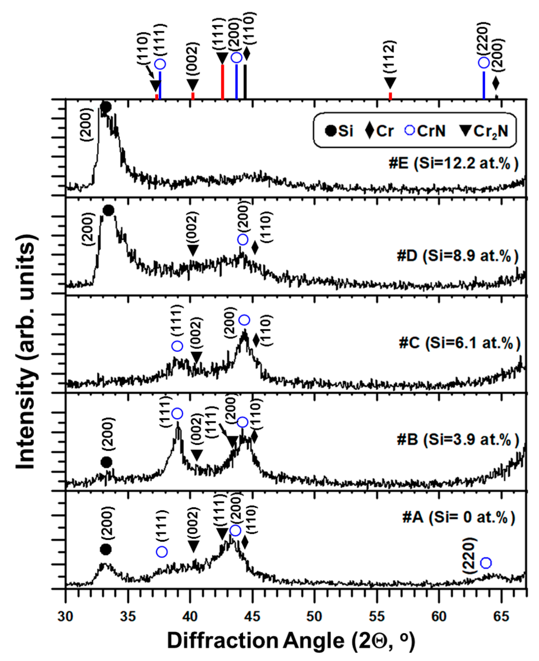
Figure 2.
Cross-sectional morphologies of as-deposited (a) #A, (b) #B, (c) #C, (d) #D, and (e) #E thin films.
Figure 2.
Cross-sectional morphologies of as-deposited (a) #A, (b) #B, (c) #C, (d) #D, and (e) #E thin films.

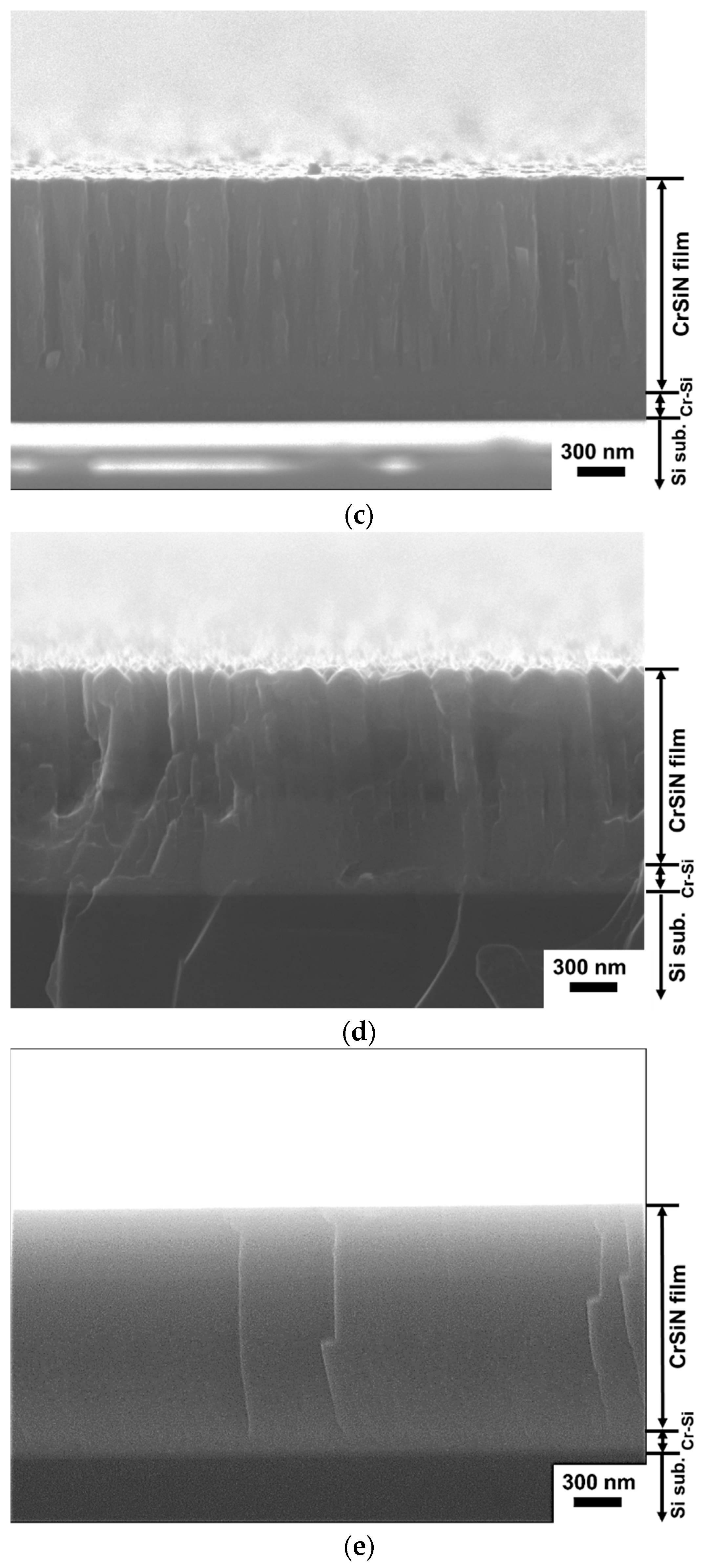
Figure 3.
Cross-sectional TEM images of as-deposited (a) #B and (b) #E thin films.

Figure 4.
The (a) weight gain of thin films and the curve of furnace heating temperature during the whole oxidation test, and (b) oxidation kinetics of thin films at 1000 °C for 6 h. The dashed fitting lines and the parabolic rate constants (unit: mg2/cm4/h) of thin films are shown in (b).
Figure 4.
The (a) weight gain of thin films and the curve of furnace heating temperature during the whole oxidation test, and (b) oxidation kinetics of thin films at 1000 °C for 6 h. The dashed fitting lines and the parabolic rate constants (unit: mg2/cm4/h) of thin films are shown in (b).

Figure 5.
The X-ray diffraction patterns of thin films after 1000 °C oxidation test.

Figure 6.
Surface morphologies of the (a) #A and (b) #E thin films after the 1000 °C oxidation test.
Figure 6.
Surface morphologies of the (a) #A and (b) #E thin films after the 1000 °C oxidation test.

Figure 7.
Cross-sectional backscattered electron images and X-ray mappings of Cr, Si, O, and N elements of the (a) #A, (b) #B, (c) #C, (d) #D, and (e) #E thin films after the 1000 °C oxidation test.
Figure 7.
Cross-sectional backscattered electron images and X-ray mappings of Cr, Si, O, and N elements of the (a) #A, (b) #B, (c) #C, (d) #D, and (e) #E thin films after the 1000 °C oxidation test.
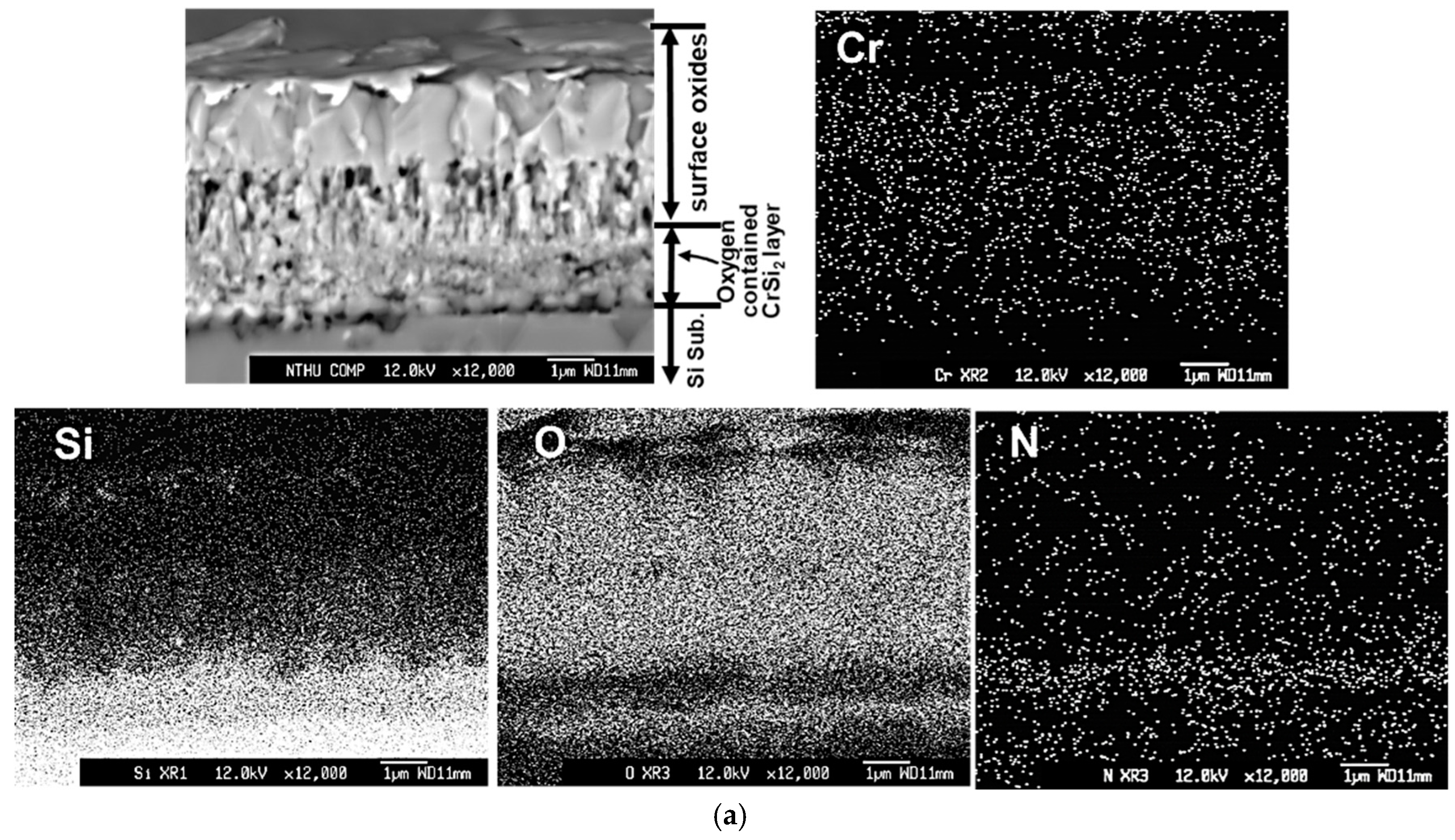
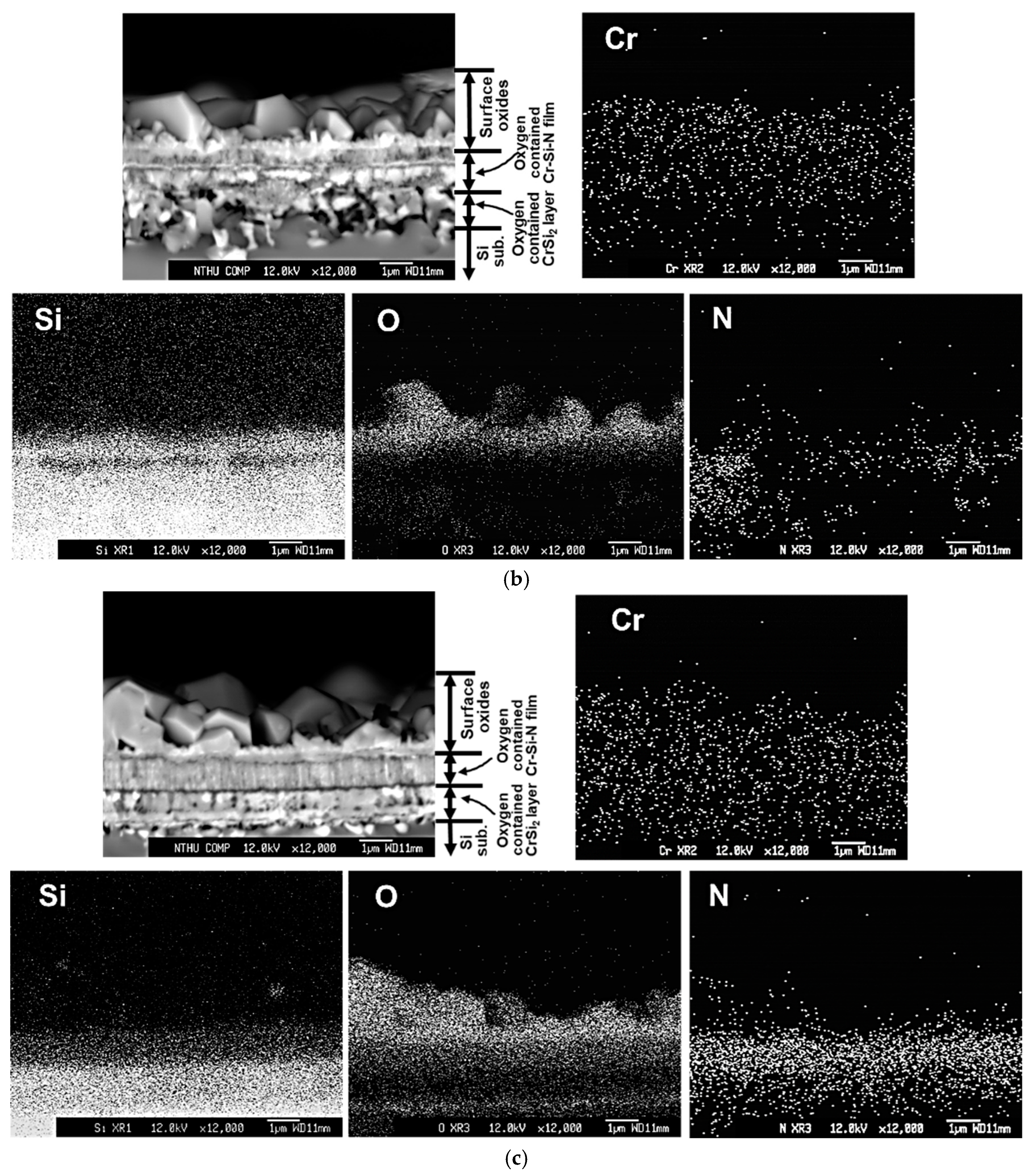

Figure 8.
The AES depth profiles of the (a) #B and (b) #E thin films after the 1000 °C oxidation test.
Figure 8.
The AES depth profiles of the (a) #B and (b) #E thin films after the 1000 °C oxidation test.


Table 1.
Deposition parameters of CrN and Cr-Si-N thin films.
| Specimen Number | #A | #B | #C | #D | #E |
|---|---|---|---|---|---|
| Cr target power (W) | 500 | 300 | 300 | 300 | 300 |
| Cr target power density (W/cm2) | 10.7 | 6.5 | |||
| Si target power (W) | 0 | 65 | 95 | 160 | 224 |
| Si target power density (W/cm2) | 0 | 1.4 | 2.1 | 3.5 | 4.9 |
| Pulsed DC condition | 20 kHz, 100% reverse voltage and 80% duty cycle | ||||
| Base pressure | 6.5 × 10⁻⁴ Pa | ||||
| Plasma etching | Ar plasma for 10 min at 2.7 Pa, substrate bias −500 V | ||||
| Interlayer | 270 nm Cr | 150 nm Cr-Si | |||
| Working pressure | 8.0 × 10⁻¹ Pa | ||||
| Ar: N2 ratio | 1:1 | ||||
| Distance between target and substrate | 100 mm | ||||
| Substrate temperature | 300 °C | ||||
| Pulsed DC substrate bias | −300 V, 80 kHz, 15% reverse voltage and 60% duty cycle | ||||
Table 2.
Chemical compositions, film thickness and residual stress of as-deposited CrNx and Cr-Si-N thin films.
Table 2.
Chemical compositions, film thickness and residual stress of as-deposited CrNx and Cr-Si-N thin films.
| Specimen Number | #A | #B | #C | #D | #E | |
|---|---|---|---|---|---|---|
| Thickness (μm) | 1.90 | 1.23 | 1.42 | 1.44 | 1.56 | |
| Chemical composition (at.%) | Cr | 58.9 | 58.0 | 55.5 | 51.2 | 53.6 |
| N | 40.7 | 38.1 | 38.4 | 38.3 | 31.1 | |
| Si | 0.0 | 3.9 | 6.1 | 8.9 | 12.2 | |
| Ar | 0.4 | 0 | 0 | 1.6 | 3.1 | |
| Si/(Cr + Si) ratio | 0 | 0.06 | 0.10 | 0.15 | 0.19 | |
| N/(Cr + Si) ratio | 0.69 | 0.62 | 0.62 | 0.64 | 0.47 | |
| Surface roughness, Ra (nm) | 6.7 | 5.0 | 4.1 | 9.1 | 1.4 | |
| Residual stress (GPa) | −0.02 | −0.09 | −0.11 | +0.24 | −0.29 | |
© 2019 by the authors. Licensee MDPI, Basel, Switzerland. This article is an open access article distributed under the terms and conditions of the Creative Commons Attribution (CC BY) license (http://creativecommons.org/licenses/by/4.0/).
Share and Cite
MDPI and ACS Style
Lou, B.-S.; Chang, Y.-C.; Lee, J.-W. High Temperature Oxidation Behaviors of CrNx and Cr-Si-N Thin Films at 1000 °C. Coatings 2019, 9, 540. https://doi.org/10.3390/coatings9090540
AMA Style
Lou B-S, Chang Y-C, Lee J-W. High Temperature Oxidation Behaviors of CrNx and Cr-Si-N Thin Films at 1000 °C. Coatings. 2019; 9(9):540. https://doi.org/10.3390/coatings9090540
Chicago/Turabian StyleLou, Bih-Show, Yue-Chyuan Chang, and Jyh-Wei Lee. 2019. "High Temperature Oxidation Behaviors of CrNx and Cr-Si-N Thin Films at 1000 °C" Coatings 9, no. 9: 540. https://doi.org/10.3390/coatings9090540
Note that from the first issue of 2016, this journal uses article numbers instead of page numbers. See further details here.