3.1. Characterization of As-Deposited Thin Films
The chemical composition of each thin film is listed in
Table 2. The Si concentration increases from 0 for #A to the highest of 12.2 at.% for #E film. The Ar contamination ranging from 0.4 to 3.1 at.% can be found for the #A, #D, and #E films. The Si/(Cr + Si) ratio of each film also increases from 0 to 0.19. It appears that the Si content increases linearly with target power of Si. The chemical stoichiometric ratio, N to Cr, of the #A films is an under-stoichiometric ratio of 0.69. Meanwhile, the chemical stoichiometric ratio, N to (Cr + Si), of four Cr-Si-N films decreases from an under-stoichiometric ratio of 0.62 to 0.47 when the Si content increase from 3.9 to 12.2 at.%.
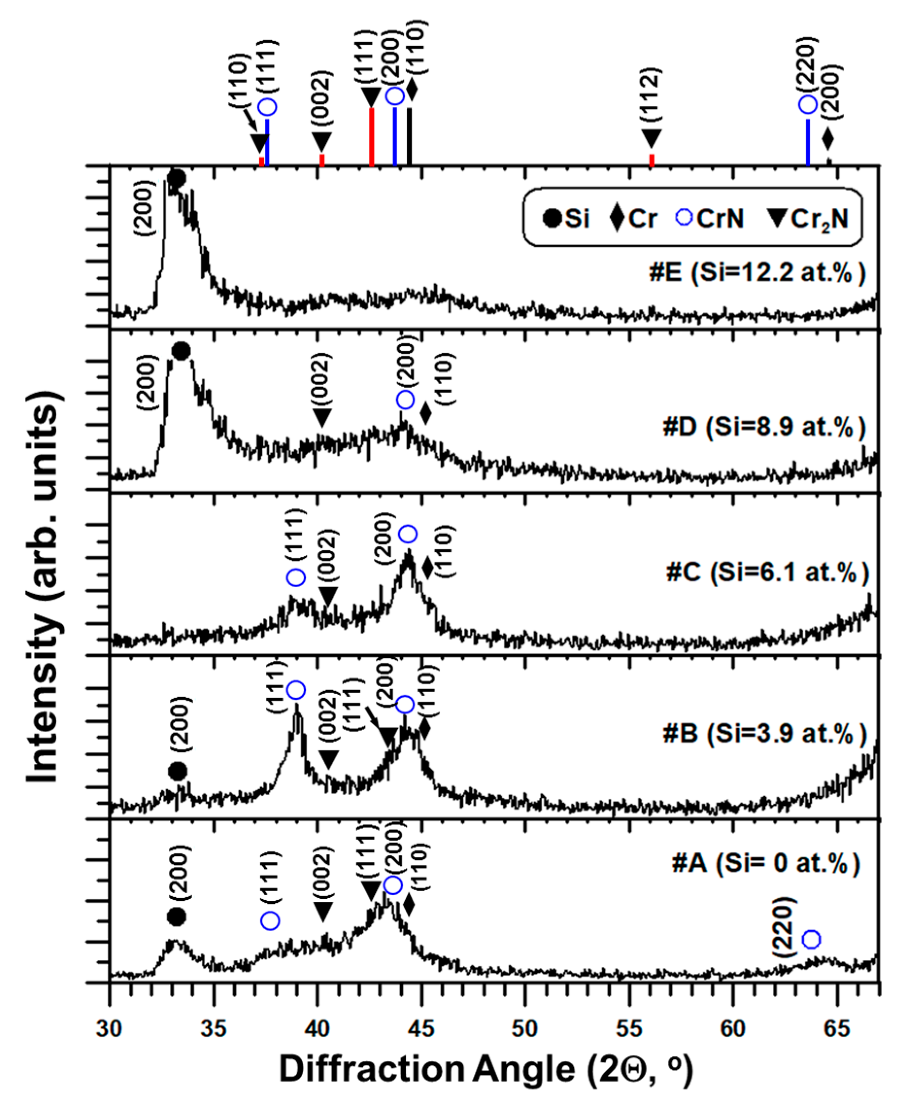
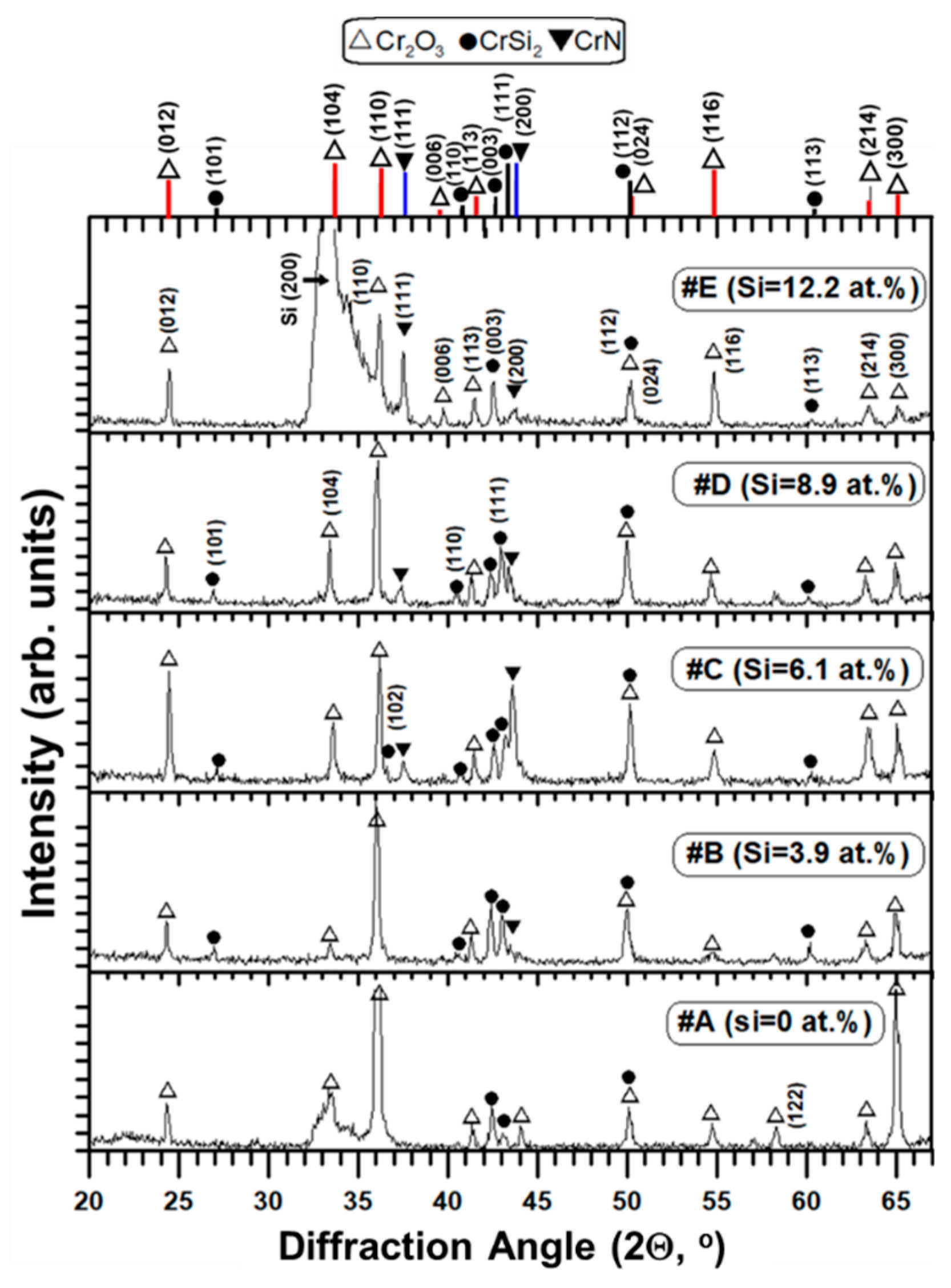
The X-ray diffraction patterns of five as-deposited thin films are shown in
Figure 1. The standard diffraction peaks of CrN (JCPDS card # 11-0065), β-Cr
2N (JCPDS card # 35-0803), and Cr (JCPDS card # 06-0694) are also indicated in
Figure 1.
A mixture of CrN and β-Cr
2N phases can be seen for the #A, #B, #C and #D films, whereas the diffraction peak corresponding to Cr or Cr-Si interlayer is also observed. However, a small hump in the range from 39° to 47° diffraction angles indicates an amorphous-like X-ray diffraction pattern for #E film containing 12.2 at.% Si. No XRD peaks corresponding to Si
3N
4 and CrSi
2 are found in
Figure 1. The CrN (111) and (200) diffraction peaks shift around 0.8°–1.2° to a higher diffraction angle in the Cr-Si-N films due to the solid solution effect of Si atoms into CrN lattice, which was reported elsewhere [
10]. The existence of Cr
2N and CrN mixed phases can be attributed to the under-stoichiometric N/(Cr + Si) ratios of 0.69 to 0.62 for the #A (CrN
x) and #B–#D (Cr-Si-N) films as listed in
Table 2. Meanwhile, the effect of Si atom acting as a substitutional solid solution element in the CrN lattice and expelling extra Cr ions to reacting with the Cr–N phase to form Cr
2N [
21,
24] is also a possible reason.
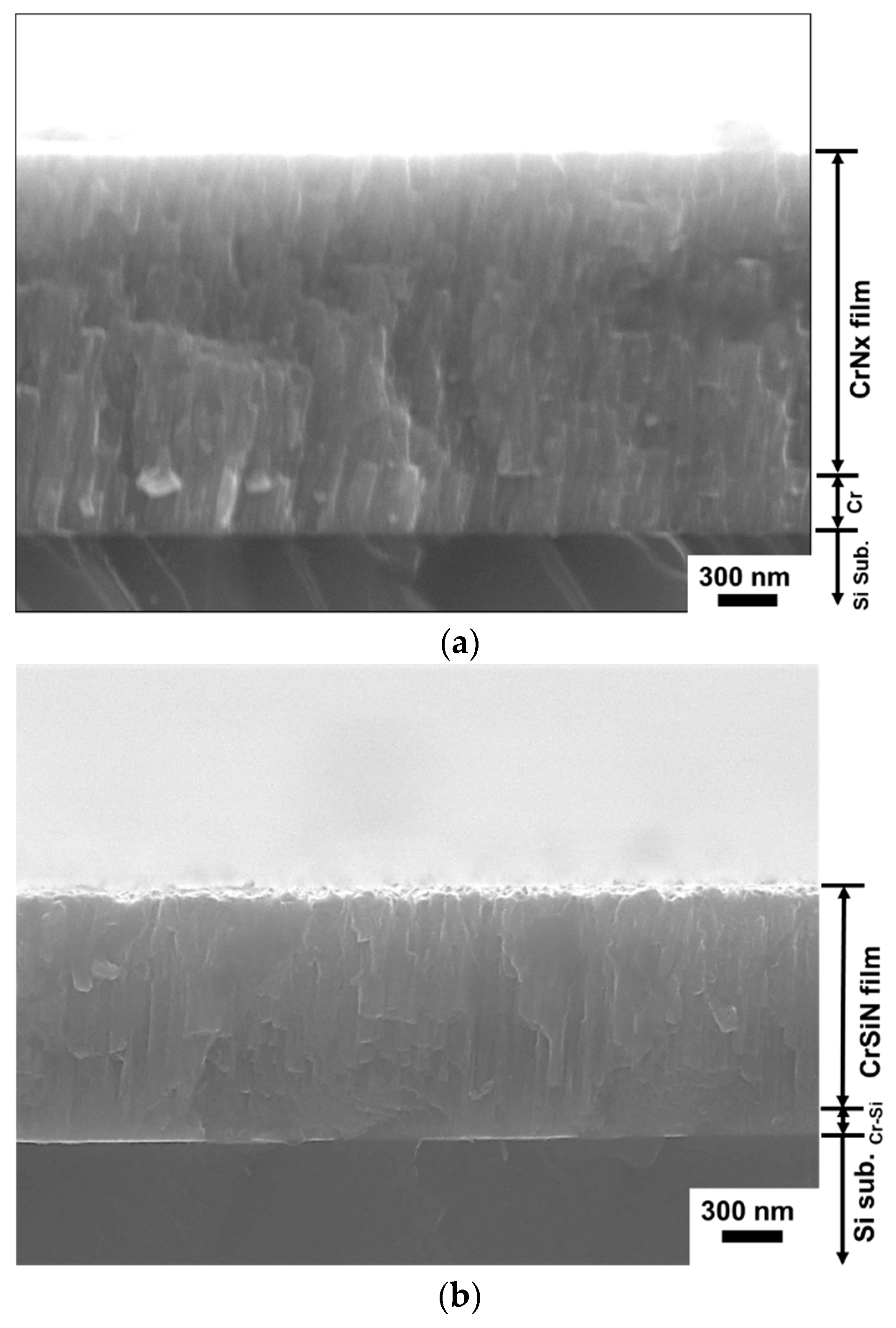
Through SEM analysis of cross-sectional microstructure of the #A thin film, as illustrated in
Figure 2a, a typical coarse columnar structure of CrN
x film and a 270 nm thick pure Cr interlayer can be seen. The width of columnar structure decreases with increasing Si content, which can be found for the #B, #C and #D films as shown in
Figure 2b–d. On the other hand, a featureless, dense, and compact morphology is observed for the #E film containing 12.2 at.% Si in
Figure 2e. The thickness of Cr-Si interlayer for each Cr-Si-N film is around 150 nm. Although the exact chemical composition of each Cr-Si layer was not measured, the microstructure of Cr-Si interlayer becomes dense and featureless, and the boundary line between the Cr-Si interlayer and Cr-Si-N film becomes ambiguous as the silicon content of Cr-Si interlayer increases, which can be seen in
Figure 2b–e. The average thickness of each thin film is measured and listed in
Table 2.
The highest thickness of 1.9 μm is obtained for the #A film due to its higher Cr target power of 500 W. In general, the Cr-Si-N film thickness increases with increasing Si content due to its higher Si target power during the sputtering process. For example, the thickness values for the #B and #E films increase from 1.23 to 1.56 μm as the Si target power and Si content increase from 65 to 224 W and from 3.9 to 12.2 at.%, respectively.
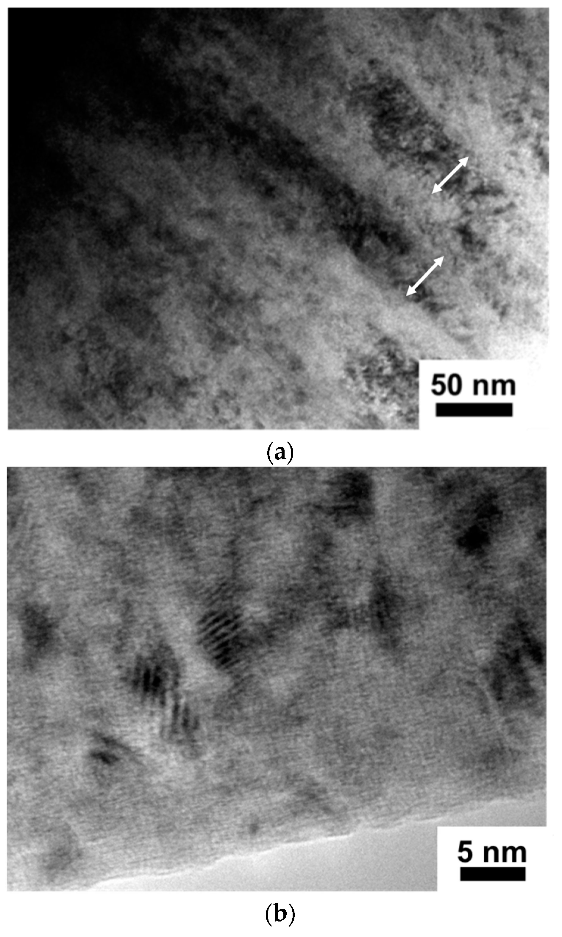
The cross-sectional images at higher magnification of the #B and #E films was analyzed by TEM, as depicted in
Figure 3a,b. It is obvious that a dense columnar microstructure, around several tens of nanometer wide as indicated by white arrows, can be found for the #B film in
Figure 3a. Meanwhile, a nanocomposite microstructure containing CrN/Cr
2N nanograins, around several nanometer in diameter, embedded in a SiNx amorphous matrix is clearly seen in
Figure 3b. The grain size refinement of Cr-Si-N film brought by the formation of the amorphous SiNx phase is confirmed in this work, which is also reported elsewhere [
22,
24,
25]. This nanocomposite microstructure is responsible for the amorphous-like XRD pattern of the #E film in
Figure 1 and the glassy cross-sectional morphology as depicted in
Figure 2e. The average surface roughness, Ra, of each thin film is listed in
Table 2. The lowest average surface roughness of 1.4 nm can be seen on the #E thin film, possibly due to its SiNx amorphous matrix. Meanwhile, the highest average surface roughness of 9.1 nm is observed for the #D film, which may be caused by the instability of substrate bias voltage during deposition.
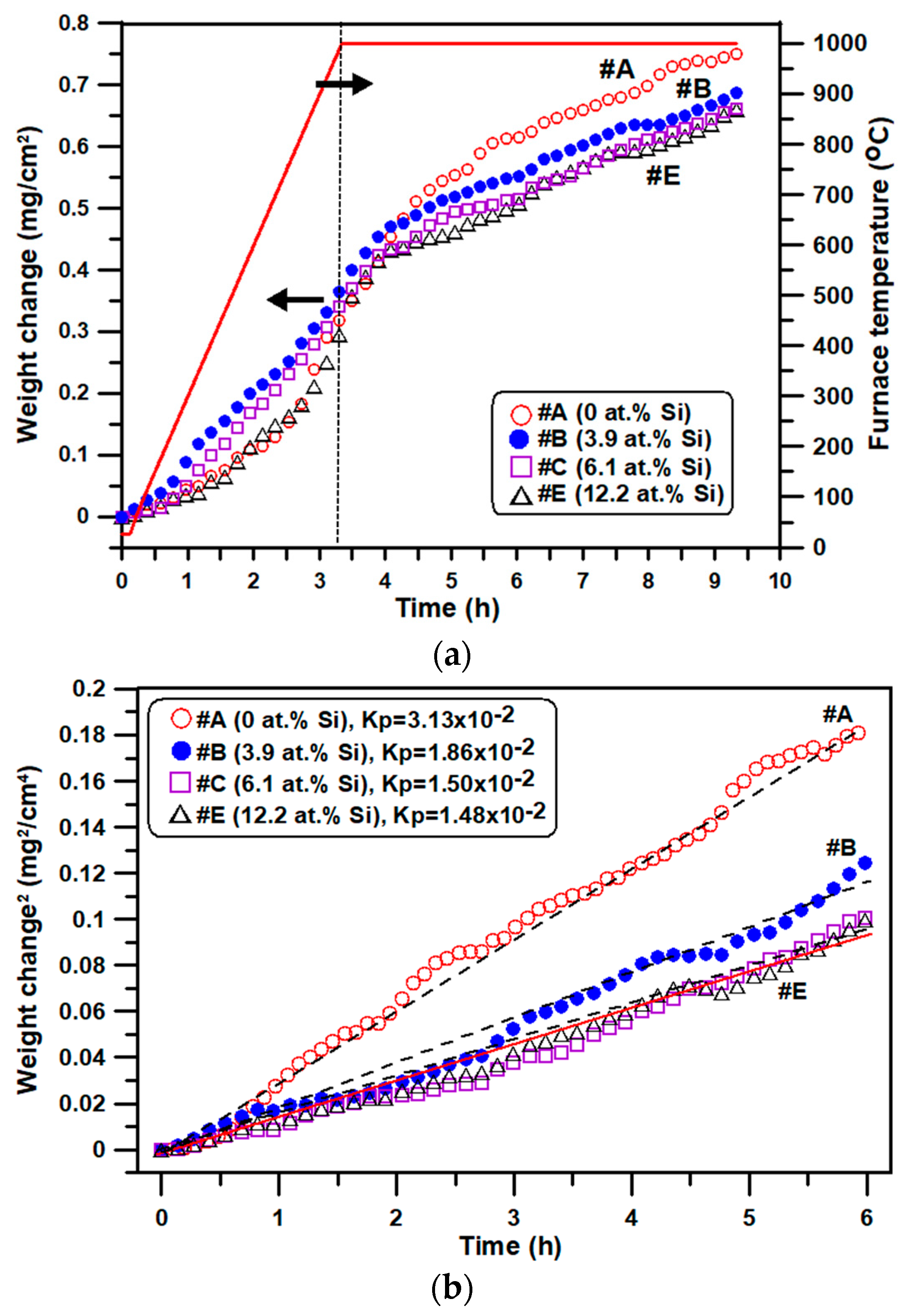
3.2. Oxidation Kinetics of Thin Films at 1000 °C
The weight gain plots of all thin films, except #D, heating from room temperature to 1000 °C and holding for 6 h are illustrated in
Figure 4a. The furnace temperature versus the heating time is also indicated by a red line. The heating time from room temperature to 1000 °C was around 3.3 h and the isothermal time at 1000 °C was 6 h. The continuous heating and isothermal heating regions are divided by a dashed line in
Figure 4a. The weight gain for each film during dynamic heating from room temperature to 1000 °C was set to zero. The weight gain of each thin film at the isothermal heating at 1000 °C for 6 h was measured again. It is important to point out that these coatings were significantly oxidized, and the weight gains were ranging from 0.31 to 0.37 mg/cm
2 before reaching 1000 °C due to a very low heating rate of 5 °C/min in air.
The relationships between the square of weight gain values versus isothermal oxidation time at 1000 °C are shown in
Figure 4b. In addition, dashed fitting lines and the calculated parabolic rate constants (unit: mg
2/cm
4/h) of four thin films are depicted in
Figure 4b.
During the heating from room temperature to 1000 °C, the #B film had the highest weight gain as compared with other thin films. On the other hand, the lowest weight gain values can be seen for the #A and #E films during the first stage of heating. We suggest that the #A film can easily form the Cr
2O
3 oxide layer on the surface for providing initial oxidation protection. After the furnace temperature was heated to 1000 °C and kept for 6 h, a rapid increase of weight gain to the highest value of 0.75 mg/cm
2 can be found for the #A film. Although the weight gain data at 1000 °C for the first hour of four thin films are very close, as shown in
Figure 4b, we can still recognize that the highest weight gain can be seen for the #A film, whereas the second highest weight gain can be found for #B film. Meanwhile, the weight gain values of #E and #C are lower and very close to each other. It is also noticed that the weight gains of the #B, #C and #E thin films are higher during dynamic heating from room temperature to 1000 °C than these during isothermal heating at 1000 °C, because of the formation of protective oxide layers during dynamic heating, which provide further oxidation resistance and less weight gain for these Si-containing films during isothermal heating at 1000 °C.
The #D film is not shown in
Figure 4 due to a severe mass loss that occurred during the heating period of the oxidation test, indicating a severe delamination of thin film. We found that a very large portion of the #D film spalled away and exhibited very poor adhesion properties on silicon substrate during heating. According to the observation of the residual stress values measured on the as-deposited thin films, as listed in
Table 2, it appears that only the #D film exhibited a tensile stress of 0.24 GPa, whereas the other films were in compressive stress states. It is reported [
26] that the total stress of an as-deposited CrN thin film is the sum of the contributions by thermal expansion, ion peening, and grain boundaries. Tensile stress is generated at grain boundaries during cooling from high deposition temperature to room temperature, whereas compressive stress is produced by ion peening [
26]. Unlike the other thin films, the ion peening effect of the #D film was not pronounced, which may have been caused by the instability of substrate bias voltage during deposition. We suggest that the compressive residual stress of thin film can compensate for the thermal stress induced from the mismatch of thermal expansion coefficients, α, between Si substrate (α
Si = 2.6 × 10
−6 K
−1 [
26]) and CrN film (α
CrN = 7.16 × 10
−6 K
−1 [
26]) during heating and cooling. On the other hand, it appears that tensile residual stress incorporated with the thermal stress peels off the thin film easily during heating.
The parabolic-like oxidation weight gain curves in
Figure 4a indicate diffusion-controlled reactions prevailed during oxidation at 1000 °C. Both the weight gains and parabolic rate constants decrease gradually with increasing Si content of Cr-Si-N thin films. It can be found that the weight gain, 0.428 mg/cm
2, and parabolic rate constant, 3.13 × 10
–2 mg
2/cm
4/h, are the highest for the #A CrN
x thin film, whereas the lowest values of 0.317 mg/cm
2 and 1.48 × 10
–2 mg
2/cm
4/h, are found for the #E film containing the highest Si content of 12.2 at.%. Apparently, high temperature oxidation resistance enhanced by the addition of Si to the CrN thin films was obtained in this study. Furthermore, the weight gain and
Kp values of the #C and #E films are almost the same, which indicates the Cr-Si-N thin films containing more than 6.1 at.% Si have similar oxidation kinetics at 1000 °C for 6 h. The parabolic oxidation behavior of CrN film at 700–900 °C and at 760–1160 °C were reported by Lin et al. [
4] and Meng and coworkers [
3], respectively. A
Kp value around 2.73 × 10
−2 mg
2/cm
4/h was calculated for the CrN film oxidized at 960 °C for 1 h [
3], which is around 13% less than that of the #A film at 1000 °C. Kim and coworkers [
9] also reported the oxidation kinetics of CrN, Cr
0.78Si
0.22N, and Cr
0.67Si
0.33N films at 800–1000 °C in air. The parabolic rate constant of Cr
0.78Si
0.22N film at 1000 °C is calculated around 4.46 × 10
–2 mg
2/cm
4/h, whereas a much higher value of 3.16 × 10
–1 mg
2/cm
4/h is calculated for the CrN film [
9]. Nevertheless, the
Kp of CrN or Cr-Si-N film at high temperature oxidation can be varied due to the difference of microstructure, chemical composition, and defect densities of thin films. It is important to point out that the
Kp value decreases with increasing Si content of Cr-Si-N film, as shown in
Figure 4b, which can provide very solid evidence for the oxidation resistance improvement by the addition of higher Si concentration in this study.
3.3. Phase and Microstructure of Thin Films after Oxidation Test at 1000 °C
The X-ray diffraction patterns of oxidized thin films are shown in
Figure 5. Since the #D film was severely delaminated during the oxidation test, the XRD analysis of the #D film was conducted using the delaminated film from the crucible.
The phases of #A are composed of Cr
2O
3 (JCPDS card # 38-1479) and CrSi
2 (JCPDS card # 35-0781). No CrN phase can be observed due to its full oxidation into the chromium oxide phase. Strong Cr
2O
3 diffraction peaks and some CrSi
2 peaks are found for the #B film as well. However, a very weak CrN (200) peak is shown around 43.7° for the #B film. For the #C, #D, and #E films, it is obvious that the primary peak is still the Cr
2O
3 (110), whereas the CrN phase can be clearly identified by the (111) peak at 37.5° and the (200) peak at 43.7°. A rather high intensity of the CrN (111) peak shown for the #E thin film indicates a higher amount of the CrN phase left after the oxidation test. In general, the CrSi
2 phase is observed in all five thin films, but no Cr
3Si phase is recognized, which was reported by Castaldi et al. [
10], in the Cr-Si-N coating oxidized at 1000 °C for 40 min. We suggest that the CrSi
2 phase observed in each thin film came from the interactions between CrN/Cr-Si-N film, Cr-Si interlayer, and Si substrate at high temperature for 6 h. However, the crystalline SiO
2 phase, which has been reported elsewhere [
8,
9,
10], is not found in this work. Based on the Gibb’s free energy calculation for the oxidation of the Cr
2N and CrN phases at 1000 °C, the reaction is favorable for the oxidation of the Cr
2N phase [
27]. According to the fact that the Cr
2N phase is absent, and only the CrN phase can be recognized in the XRD results in
Figure 5 for four Si-containing films after oxidation at 1000 °C, we therefore suggest that this phase evolution is possibly due to the preferential oxidation of the Cr
2N phase and an increased depletion of Cr element of the Cr
2N phase.
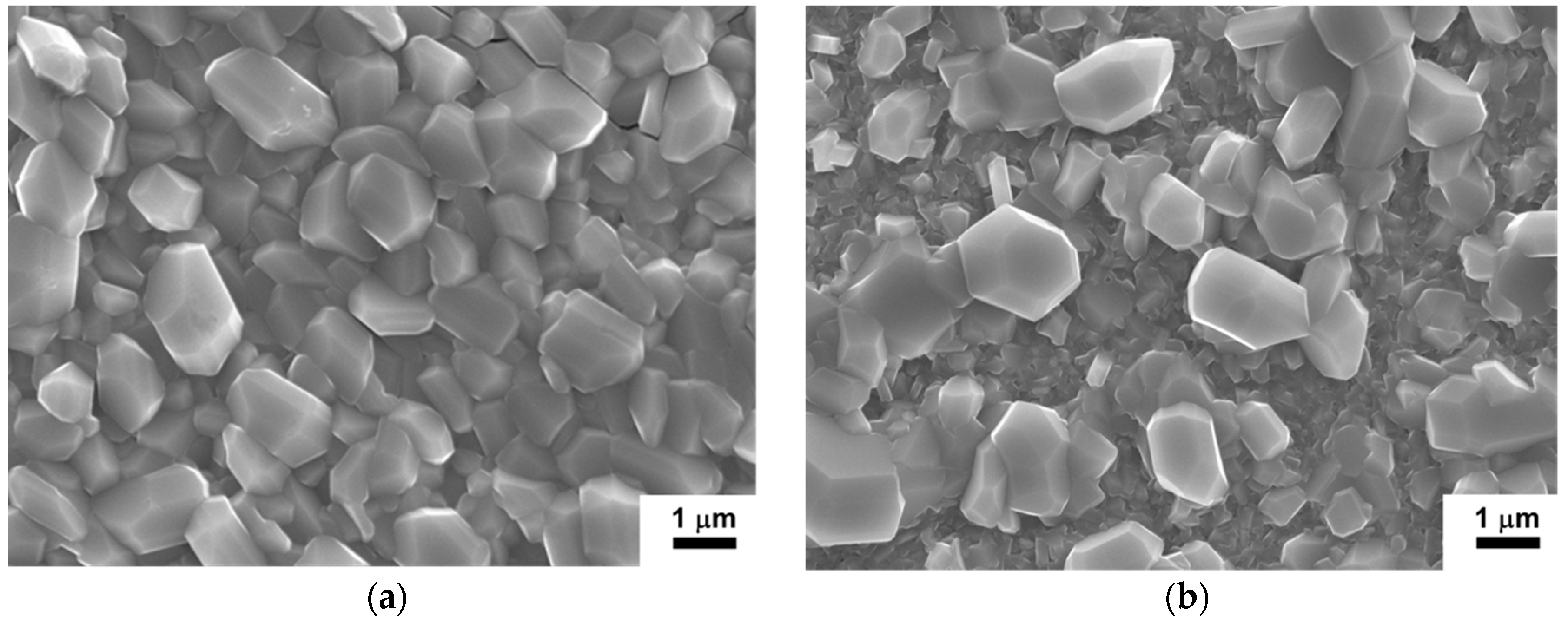
The surface morphology of the oxidized #A thin film, as shown in
Figure 6a, exhibits large faceted grains, which can be confirmed as Cr
2O
3 by FE-EPMA analysis and XRD results. The grain size of Cr
2O
3 is around 1–3 μm in diameter. On the other hand, the surface morphology of the oxidized #E film is shown in
Figure 6b. The number of faceted Cr
2O
3 grains decreases as Si content increases to 12.2 at.%. A very dense Si-containing oxide layer with a smaller grain size can be found under the faceted grains. Apparently, the dense Si-containing oxide layer beneath the large surface Cr
2O
3 grains becomes a protective layer to the thin film. It was reported that Cr oxidizes faster than Si due to the strong covalent bonding of amorphous silicon nitride, which restricts the outward diffusion of Si [
10]. After the oxidation of Cr, the amorphous SiNx phase and Si atoms dissolved in CrN structures start to oxidize into amorphous silicon oxide, which can impinge both outward and inward diffusion paths of other elements [
8].
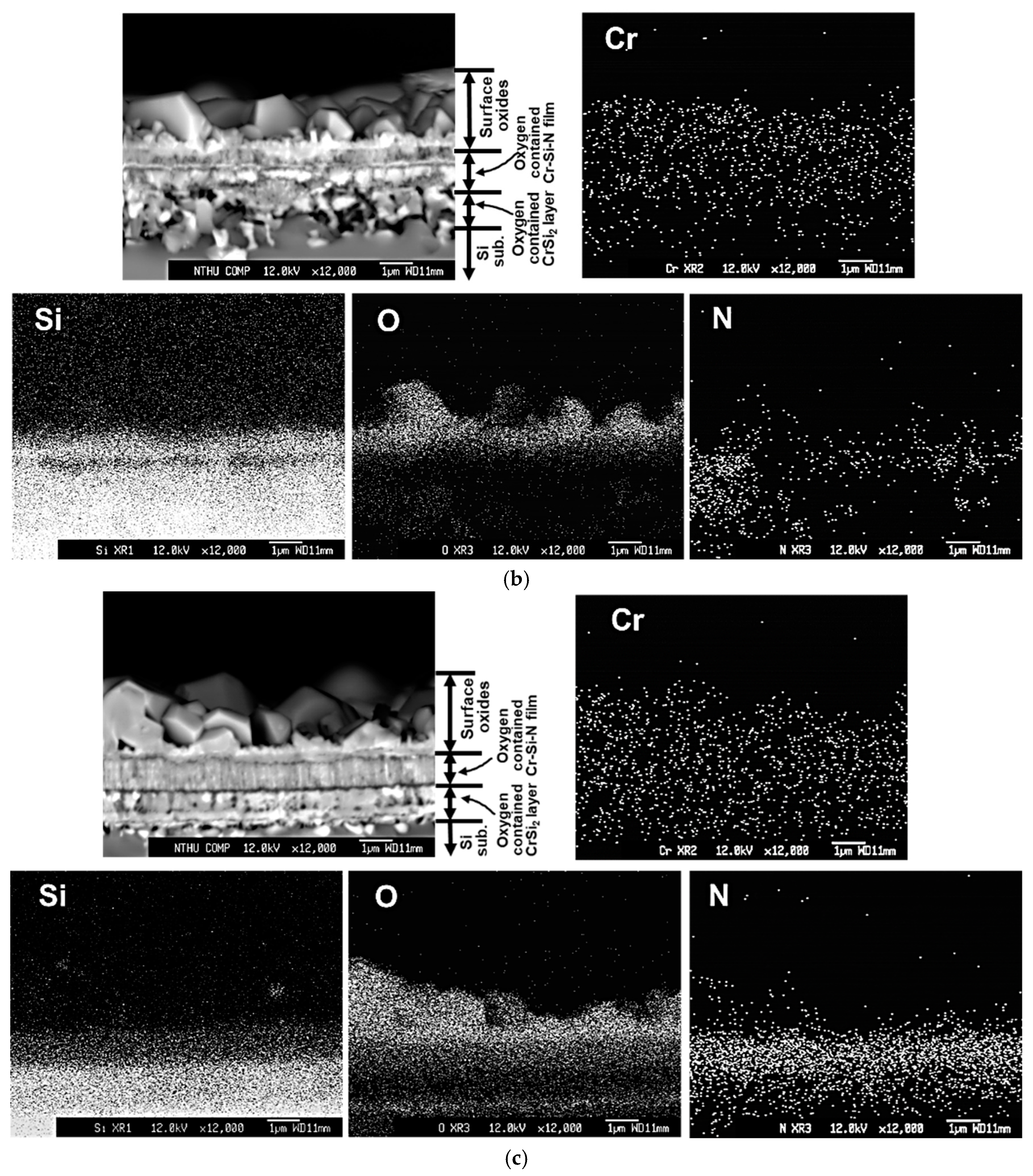
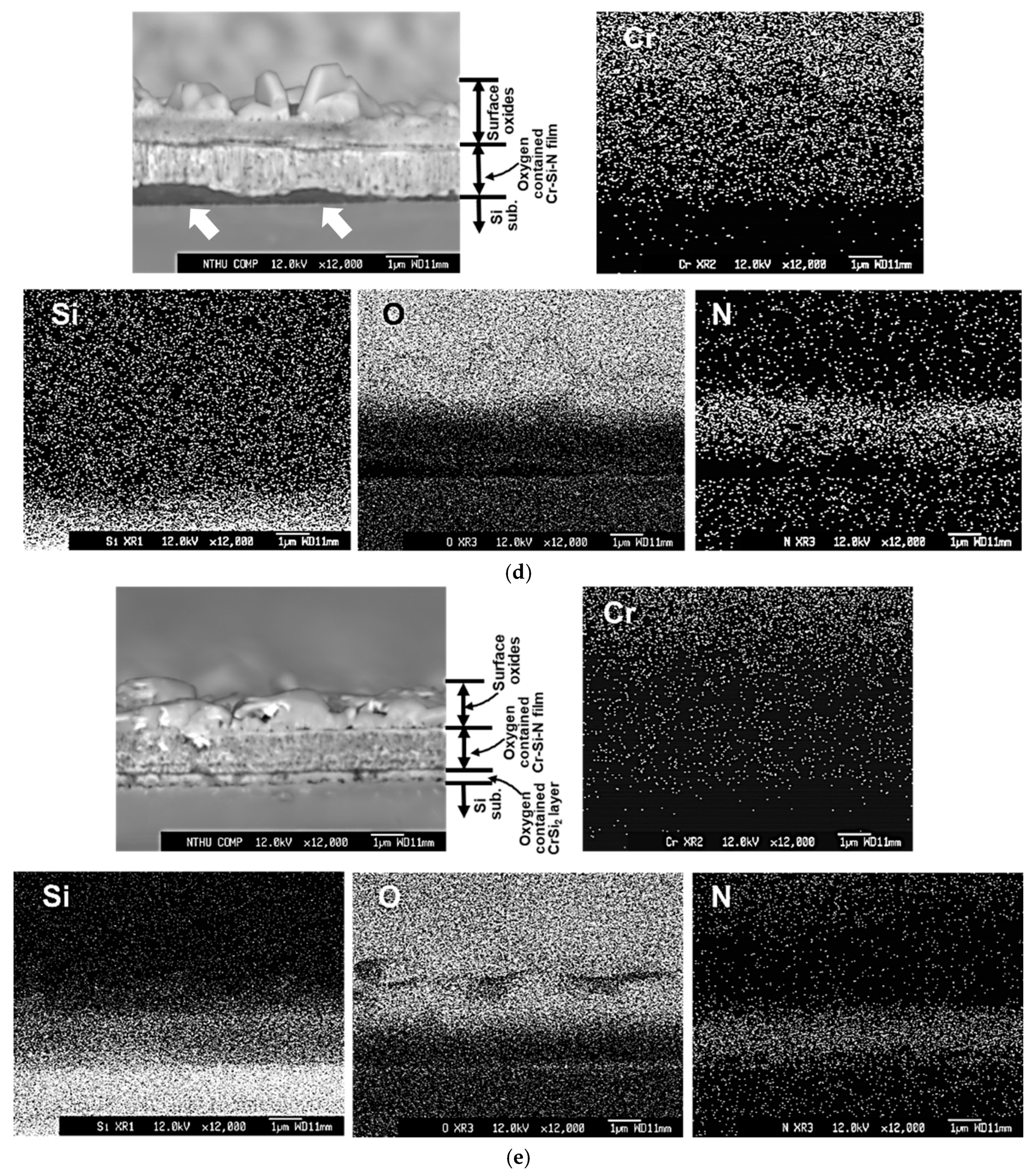
Figure 7 depicts the cross-sectional backscattered electron images and X-ray mappings of Cr, O, Si, and N elements by FE-EPMA of all thin films after the oxidation test. Since the #D film was almost delaminated after the oxidation test, the cross-sectional image of #D was taken from the retained film, which was still adhered on the Si substrate. The outermost oxide layer, remaining oxygen-containing Cr-Si-N nitride layer, oxygen-containing CrSi
2 region, and Si substrate are indicated for each film in
Figure 7. In
Figure 7a, the whole CrN
x film was almost totally oxidized, which can be confirmed by the X-ray mapping of O. It is obvious that a dense Cr
2O
3 oxide layer around 2.6 μm thick is formed on the outermost surface region, whereas a porous oxide zone around 1.5 μm in thickness is measured between the Cr
2O
3 surface layer and the inner granular structured oxygen-containing CrSi
2 region, as shown in
Figure 7a. This porous structure is full of voids, which were possibly formed due to the rapid outward diffusion of Cr and N atoms and inward diffusion of O atoms during high temperature oxidation. Lin and coworkers [
4] also discovered a similar porous microstructure in the CrN film after oxidation at 1000 °C for 1 h in air. The phase transformation of Cr
2N to CrN during high temperature oxidation is also attributed to the formation of voids [
27]. According to the X-ray mappings of N and O, very small amounts of nitrogen and oxygen concentrations can be seen in the upper and lower region of the CrSi
2 layer. Since the melting point of Si is around 1440 °C, the diffusion reaction of Si plays an important role in the formation of the CrSi
2 phase during oxidation at 1000 °C. Therefore, the original thin Cr interlayer was further reacted with Si substrate and became a granular oxygen- and nitrogen-containing CrSi
2 region because of the poor oxidation resistance of CrN
x film.
In
Figure 7a, the thickness of the porous nitrogen- and oxygen-containing CrSi
2 region is around 1.6 μm, possibly due to the severe interdiffusion of Si, N and O elements in this region at high temperature. This CrSi
2 region is also full of voids, which also make the layer thickness become thicker. For the #B films, as shown in
Figure 7b, faceted Cr
2O
3 grains can be found on the surface oxide layer, which is around 2.4 μm thick. A complex porous morphology is observed in the oxygen- and nitrogen-containing CrSi
2 phase region with a thickness around 1.5 μm. Some voids, oxides, and needle-like CrSi
2 phases penetrating the Si substrate indicate that complex reactions occurred between the original thin Cr-Si interlayer and Si substrate during 1000 °C heating. Based on the X-ray mapping of N, the oxygen-containing Cr-Si-N film becomes discontinuous and porous. The estimated thickness of this porous Cr-Si-N layer is around 1.0 μm, as depicted in
Figure 7b. On the other hand, layered microstructures are observed for the #C, #D, and #E films, as illustrated in
Figure 7c–e. According to the backscattered electron image (BEI) micrographs and the corresponding X-ray mappings of N, the remaining thickness values of the oxygen-containing Cr-Si-N layer for the #C, #D, and #E films are around 0.9, 1.4 and 1.3 μm, respectively. The remaining oxygen-containing Cr-Si-N layer of the #C film shows a columnar microstructure. As compared with the oxygen-containing Cr-Si-N structures in
Figure 7c–e, a more compact microstructure can be found for the #D and #E films. For the #C and #E films, the thickness values of the porous oxygen-containing CrSi
2 phase regions are around 0.9 and 0.27 μm thick, respectively. However, almost no CrSi
2 phase region can be found for the #D film, possibly due to the delamination of thin film from the Si substrate, as indicated by the arrows in
Figure 7d. Besides, a very small amount of oxygen content can be seen in the CrSi
2 phase region in
Figure 7e, implying a good oxidation resistance of the #E film at 1000 °C. The thicknesses of the CrSi
2 phase regions for the #A, #B, #C and #E films are different as the oxidation resistance of these thin films are different. A better oxidation resistance of Cr-Si-N thin film can decrease the inward/outward diffusion reactions of O and Si, and lowers the amount of voids and reduces the thickness of such CrSi
2 phase regions. Although the parabolic rate constant values of the #C and #E films are very close, we can still confirm that a better oxidation resistance can be seen for the #E film due to its dense microstructure, thicker remaining Cr-Si-N layer (around 1.3 μm), and a thin and relatively low oxygen-containing CrSi
2 interlayer (around 0.27 μm in thickness) after the oxidation test.
We believe that the amorphous silicon nitride matrix of the nanocomposite microstructure of the #E film plays an important role for effectively blocking the outward and inward diffusion of Cr, N, Si and O elements during high temperature oxidation. It is also important to point out that a continuous Si-rich oxide layer can be observed between the surface oxide layer and the the #E Cr-Si-N film layer, as depicted in
Figure 7e. This microstructure provides solid evidence for its good oxidation resistance at 1000 °C for 6 h. There are two factors that can affect the performance of the CrN
x and Cr-Si-N thin films during high temperature oxidation testing; one is the residual stress state in the as-deposited film, and the other is the Si content of Cr-Si-N film. Apparently, increasing the amount of Si content, for example, higher than 8.9 at.%, enhances the high temperature oxidation resistance of Cr-Si-N thin film. However, the residual tensile stress, such as the #D film in this study, shows a detrimental effect on the adhesion properties of thin film and thus eliminates the advantage of high Si content for oxidation resistance improvement.
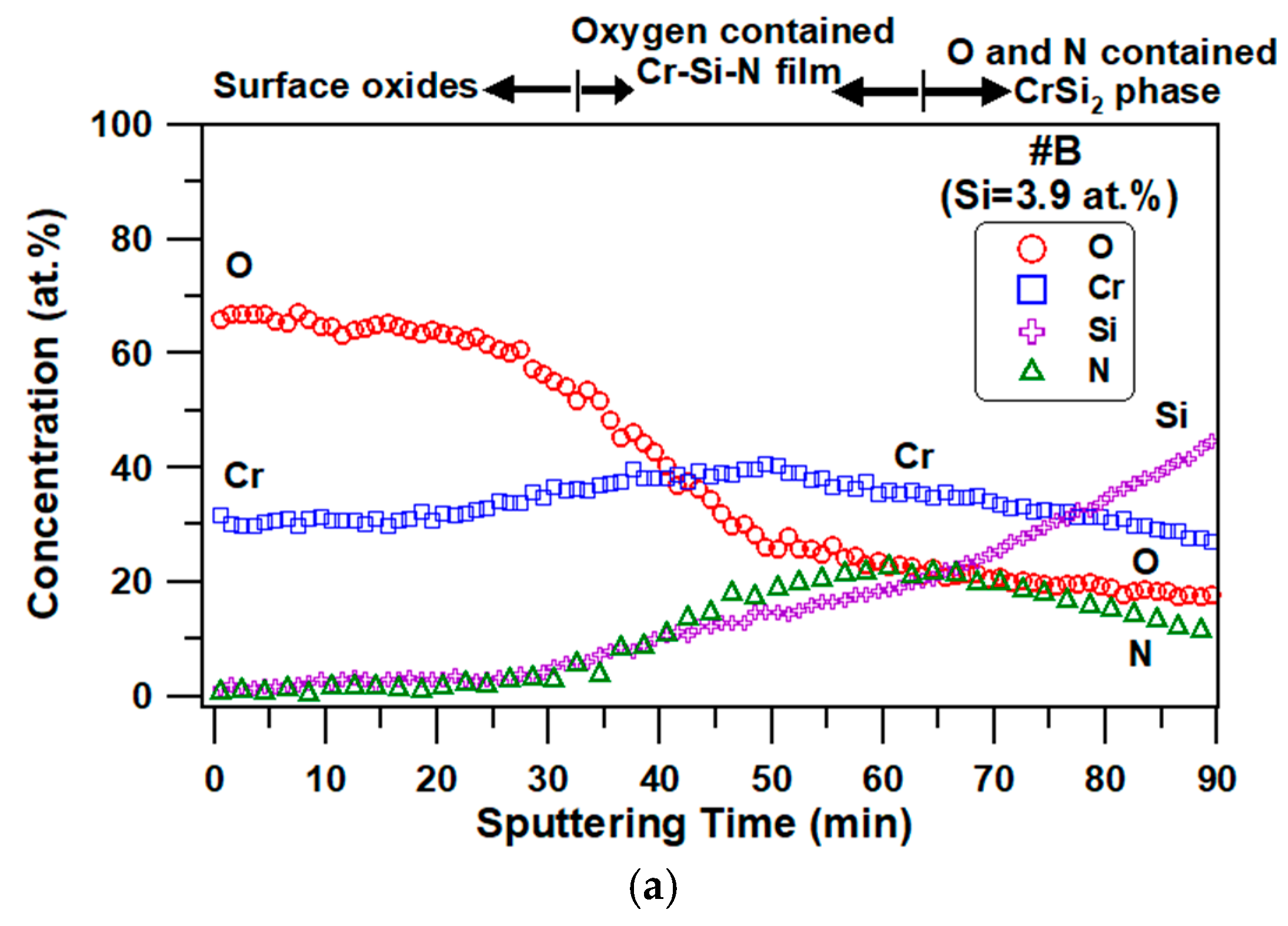
The AES depth profiles of the oxidized #B and #E films are depicted in
Figure 8a,b, respectively. Estimated structure evolutions of thin films are also drawn based on the concentration profiles and XRD results in
Figure 5. For the #B film, it is obvious that an inward diffusion of oxygen is shown, while the outward diffusions of Cr, N, and Si are revealed. A thick Cr
2O
3 oxide region is formed on the surface based on the chemical composition analysis data shown in
Figure 8a, which is also consistent with the microstructure observation and the X-ray mapping of O element in
Figure 7b.
Based on the O and N profiles, the oxygen content reaches 24 at.% in the Cr-Si-N film of #B. The higher Si concentration, around 10–20 at.%, in the thin film is attributed to the outward diffusion of Si atoms from the 150-nm-thick Cr-Si interlayer and Si substrate. It is important to point out that the AES depth profile of the oxidized #B film does not reach the Si substrate after sputter etching for 90 min due to its extremely large thickness, around 4.9 μm, as illustrated in the BEI micrograph in
Figure 7b.
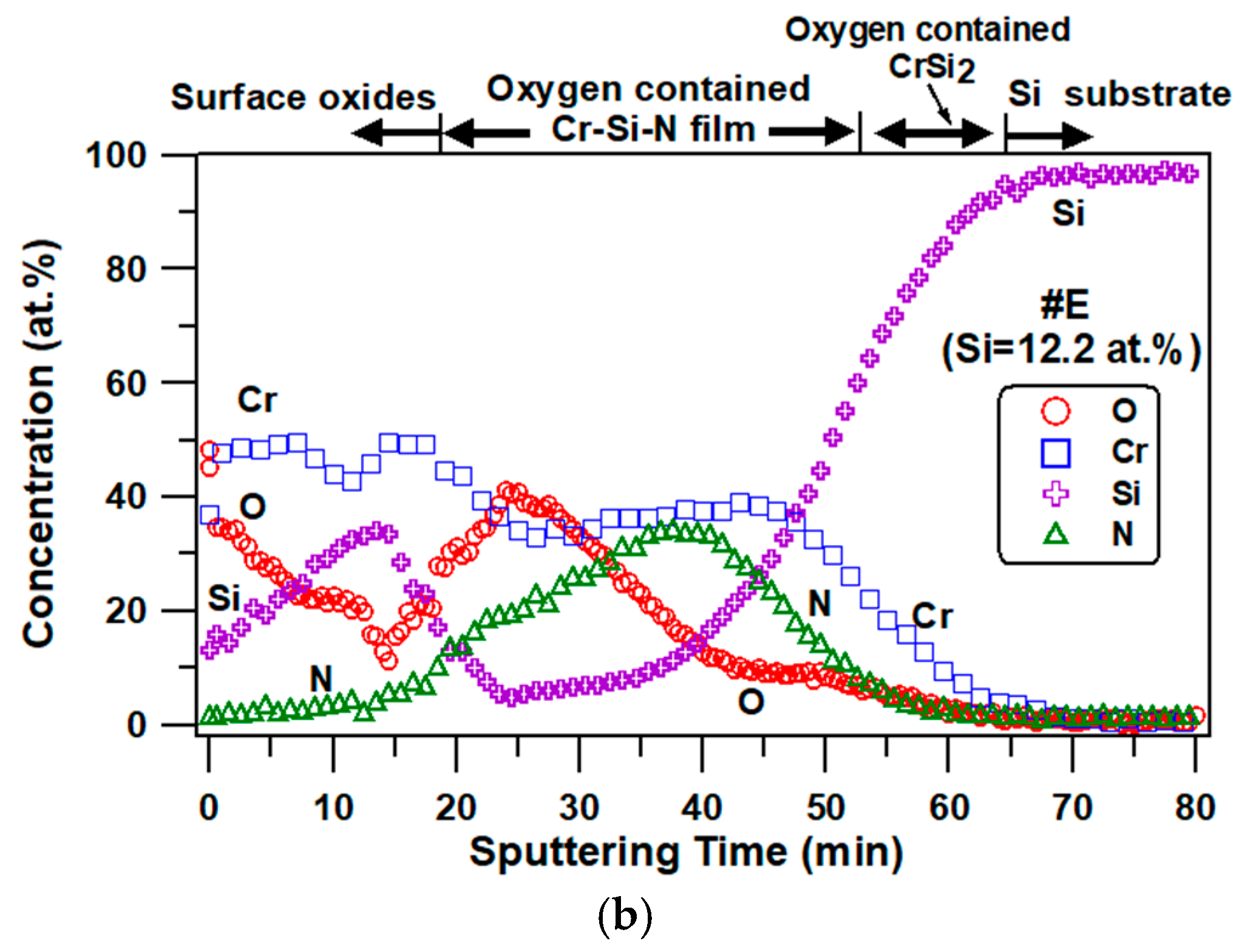
Figure 8b illustrates the AES depth profiles of the #E film, where a rather complex concentration profiling of elements is observed as compared with that of the #B film. The Si substrate and the CrSi
2 layer are recognized in
Figure 8b. The outer surface is rich in Cr and O, and is depleted in N, indicating an oxide layer containing around 12 at.% Si was formed, which corresponds to the dense surface oxide layer as shown in
Figure 7e. The average chemical composition of the outermost oxide region is 38.7% Cr, 46.8% O, 12.8% Si and 1.7% N (in at.%), which deviates from the chemical composition of Cr
2O
3 oxide. We suggest that this chemical deviation can be attributed to the partial spallation of the outermost Si-containing Cr
2O
3 oxide layer. In addition, the higher surface roughness brought by the large crystallites on the oxidized surface can affect the accuracy of chemical analysis of AES. A silicon concentration pile-up layer, reaching around 35 at.%, is discovered in the region between the surface oxide and CrSiN film, indicating a high Si-containing amorphous silicon oxide layer, which can retard the diffusion paths of O, Cr, and N. A similar finding of the Si and O-rich layer can be observed in the X-ray mappings of Si and O in
Figure 7e. The N content in the Cr-Si-N film ranges from 15 to 34 at.%, which is lower than that before oxidation. On the other hand, the Si content varies from 6 to 42 at.% in the Cr-Si-N film, which is attributed to the outward diffusion of Si from the Cr-Si interlayer and Si substrate. The O content decreases gradually from 40 to 8 at.% in the Cr-Si-N film. In the literature, the oxidation resistance of CrSiN [
8,
9,
10,
11], CrAlN, and CrAlSiN films [
17,
19,
20] at high temperature were greatly improved by the adequate amount of Si added. The improvement mechanism by the formation of an amorphous silicon oxide layer is also valid in this study. Finally, we can conclude that the higher Si-containing Cr-Si-N film enhanced its oxidation resistance due to the formation of dense surface Cr
2O
3 layer and the amorphous silicon oxide layer for retarding the outward and inward diffusion reactions at 1000 °C. Even a very similar parabolic rate constant was obtained for the #C and #E films; the best oxidation resistance of the #E film containing 12.2 at.% Si can be confirmed by its dense microstructure in
Figure 7e and the AES analysis in
Figure 8b.


