Ohmic Contact of Pt/Au on Hydrogen-Terminated Single Crystal Diamond


Abstract
:1. Introduction
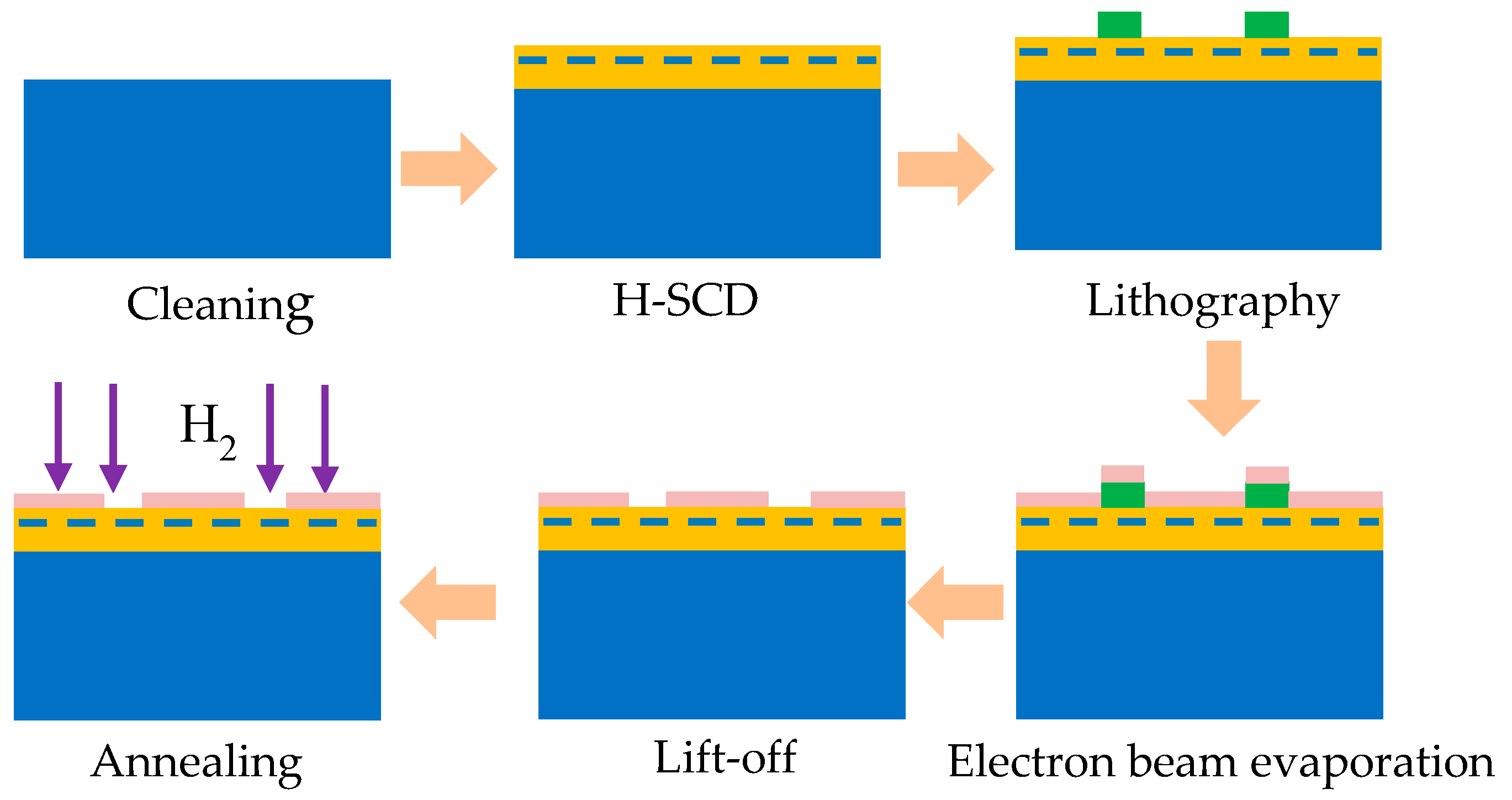
2. Experiment
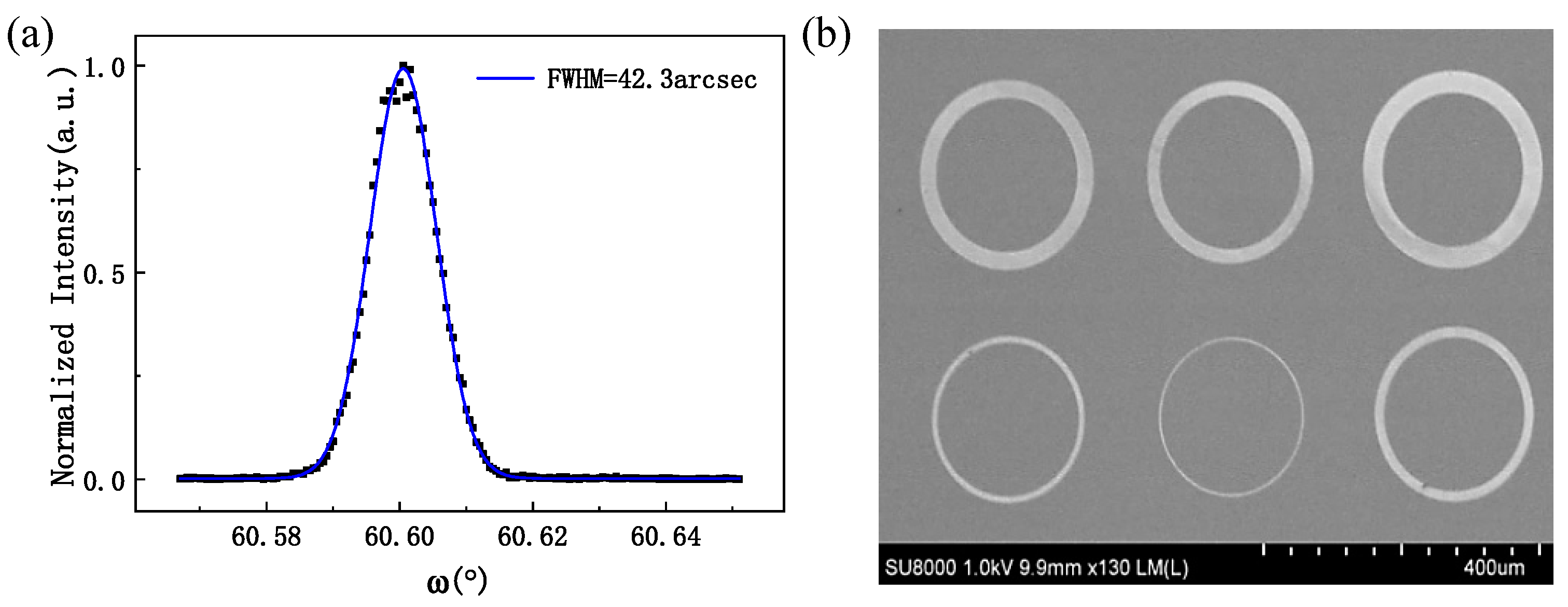
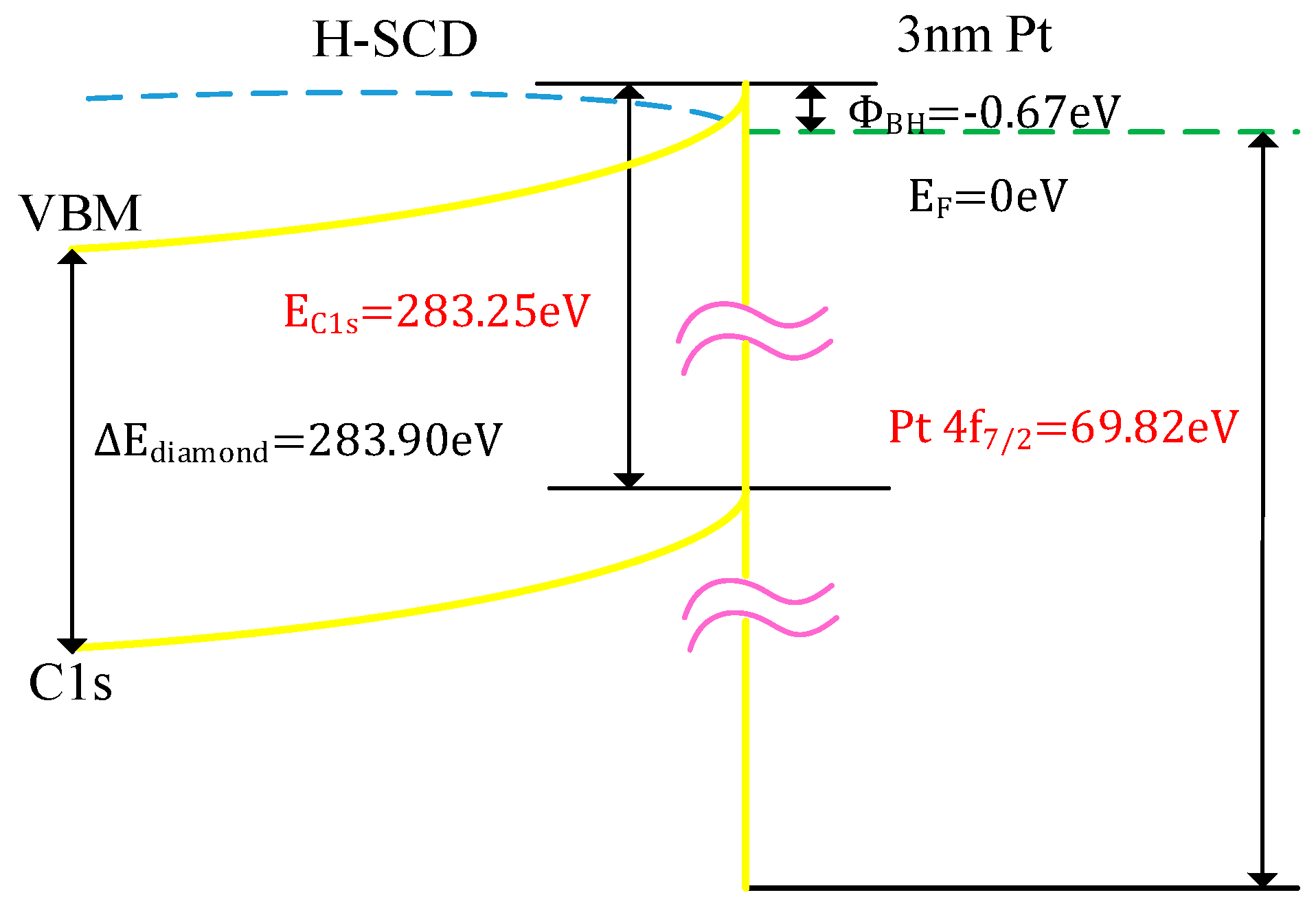
3. Result and Discussion
4. Conclusions
Author Contributions
Funding
Conflicts of Interest
References
- Isberg, J.; Hammersberg, J.; Johansson, E.; Wikstrom, T.; Twitchen, D.J.; Whitehead, A.J.; Coe, S.E.; Scarsbrook, A. High carrier mobility in single-crystal plasma-deposited diamond. Science 2002, 297, 1670–1672. [Google Scholar] [CrossRef] [PubMed]
- Ekimov, E.A.; Sidorov, V.A.; Bauer, E.D.; Melnik, N.N.; Curro, N.J.; Thompson, J.D.; Stishov, S.M. Superconductivity in diamond. Nature 2004, 428, 542–545. [Google Scholar] [CrossRef] [PubMed] [Green Version]
- Kalish, R. Diamond as a unique high-tech electronic material: Difficulties and prospects. J. Phys. D. Appl. Phys. 2007, 40, 6467–6478. [Google Scholar] [CrossRef]
- Baliga, B.J. Power Semiconductor Devices; PWS Publishing Company: Boston, MA, USA, 1995. [Google Scholar]
- Umezawa, H.; Shikata, S.; Funaki, T. Diamond Schottky barrier diode for high-temperature, high-power and fast switching applications. Jpn. J. Appl. Phys. 2014, 53, 05FP06. [Google Scholar] [CrossRef]
- Vescan, A.; Daumiller, I.; Gluche, P.; Ebert, W.; Kohn, E. High temperature, high voltage operation of diamond Schottky diode. Diam. Relat. Mater. 1998, 7, 581–584. [Google Scholar] [CrossRef]
- Umezawa, H.; Tokuda, N.; Ogura, M.; Ri, S.; Shikata, S. Characterization of leakage current on diamond Schottky barrier diodes using thermionic-field emission modeling. Diam. Relat. Mater. 2006, 15, 1945–1953. [Google Scholar] [CrossRef]
- Traore, A.; Muret, P.; Fiori, A.; Eon, D.; Gheeraert, E.; Pernot, J. Zr/oxidized diamond interface for high power Schottky diodes. Appl. Phys. Lett. 2014, 104, 052105. [Google Scholar] [CrossRef]
- Kawarada, H. High-current metal oxide semiconductor field-effect transistors on H-terminated diamond surfaces and their high-frequency operation. Jpn. J. Appl. Phys. 2012, 51, 090111. [Google Scholar] [CrossRef]
- Liu, J.W.; Liao, M.Y.; Imura, M.; Oosato, H.; Watanabe, E.; Koide, Y. Electrical characteristics of hydrogen-terminated diamond metal-oxide-semiconductor with atomic layer deposited HfO2 as gate dielectric. Appl. Phys. Lett. 2013, 102, 112910. [Google Scholar] [CrossRef]
- Wang, W.; Fu, K.; Hu, C.; Li, F.N.; Liu, Z.C.; Li, S.Y.; Lin, F.; Fu, J.; Wang, J.J.; Wang, H.X. Diamond based field-effect transistors with SiNx and ZrO2 double dielectric layers. Diam. Relat. Mater. 2016, 69, 237–240. [Google Scholar] [CrossRef]
- Jingu, Y.; Hirama, K.; Kawarada, H. Ultrashallow TiC source/drain contacts in diamond MOSFETs formed by hydrogenation-last approach. IEEE Trans. Electron. Devices 2010, 57, 966–972. [Google Scholar] [CrossRef]
- Isberg, J.; Hammersberg, J.; Twitchen, D.J.; Whitehead, A.J. Single crystal diamond for electronic applications. Diam. Relat. Mater. 2004, 13, 320–324. [Google Scholar] [CrossRef]
- Wen, F.; Zhang, X.; Ye, H.; Wang, W.; Wang, H.; Zhang, Y.; Dai, Z.; Qiu, C.W. Efficient and tunable photoinduced honeycomb lattice in an atomic ensemble. Laser Photonics Rev. 2018, 12, 1800050. [Google Scholar] [CrossRef]
- Nebel, C.E. Chemistry. Surface-conducting diamond. Science 2007, 318, 1391–1392. [Google Scholar] [CrossRef] [PubMed]
- Kawarada, H. Hydrogen-terminated diamond surfaces and interfaces. Surf. Sci. Rep. 1996, 26, 205–259. [Google Scholar] [CrossRef]
- Nebel, C.E.; Sauerer, C.; Ertl, F.; Stutzmann, M.; Graeff, C.F.O.; Bergonzo, P.; Williams, O.A.; Jackman, R. Hydrogen-induced transport properties of holes in diamond surface layers. Appl. Phys. Lett. 2001, 79, 4541–4543. [Google Scholar] [CrossRef]
- Kawarada, H.; Yamada, T.; Xu, D.; Kitabayashi, Y.; Shibata, M.; Matsumura, D.; Kobayashi, M.; Saito, T.; Kudo, T.; Inaba, M.; et al. Diamond MOSFETs Using 2D Hole Gas with 1700V Breakdown Voltage. In Proceedings of the International Symposium on Power Semiconductor Devices & Ics., Prague, Czech Republic, 12–16 June 2016. [Google Scholar]
- Kawarada, H.; Aoki, M.; Sasaki, H.; Tsugawa, K. Characterization of hydrogen-terminated CVD diamond surfaces and their contact properties. Diam. Relat. Mater. 1994, 3, 961–965. [Google Scholar] [CrossRef]
- Wang, W.; Hu, C.; Li, F.N.; Li, S.Y.; Liu, Z.C.; Wang, F.; Fu, J.; Wang, H.X. Palladium Ohmic contact on hydrogen-terminated single crystal diamond film. Diam. Relat. Mater. 2015, 59, 90–94. [Google Scholar] [CrossRef]
- Wang, Y.F.; Chang, X.; Li, S.; Zhao, D.; Shao, G.; Zhu, T.; Fu, J.; Zhang, P.; Chen, X.; Li, F.; et al. Ohmic contact betweent iridium film and hydrogen-terminated single crystal diamond. Sci. Rep. 2017, 7, 12157. [Google Scholar] [CrossRef]
- Wang, W.; Hu, C.; Li, S.Y.; Li, F.N.; Liu, Z.C.; Wang, F.; Fu, J.; Wang, H.X. Diamond based field-effect transistors of Zr gate with SiNx dielectric layers. J. Nanomater. 2015, 2015, 10. [Google Scholar] [CrossRef]
- Banal, R.G.; Imura, M.; Liu, J.; Koide, Y. Structural properties and transfer characteristics of sputter deposition AlN and atomic layer deposition Al2O3, bilayer gate materials for H-terminated diamond field effect transistors. J. Appl. Phys. 2016, 120, 115307. [Google Scholar] [CrossRef]
- Wang, Y.F.; Wang, W.; Chang, X.; Zhang, X.; Fu, J.; Liu, Z.; Zhao, D.; Shao, G.; Fan, S.; Bu, R.; et al. Hydrogen terminated diamond field-effect transistor with AlOx dielectric layer formed byautoxidation. Sci. Rep. 2019, 9, 5192. [Google Scholar] [CrossRef] [PubMed]
- Zhen, C.M.; Wang, X.Q.; Wu, X.C.; Liu, C.X.; Hou, D.L. Au/p-diamond ohmic contacts deposited by RF sputtering. Appl. Surf. Sci. 2008, 255, 2916–2919. [Google Scholar] [CrossRef]
- Wahab, Q.; Macak, E.B.; Zhang, J.; Madsen, L.D.; Janzen, E. Improvements in the electrical performance of high voltage 4H-SiC Schottky diodes by hydrogen annealing. Mater. Sci. Forum 2001, 353, 691–694. [Google Scholar] [CrossRef]
- Li, F.N.; Liu, J.W.; Zhang, J.W.; Wang, X.L.; Wang, W.; Liu, Z.C.; Wang, H.X. Measurement of barrier height of Pd on diamond (100) surface by X-ray photoelectron spectroscopy. Appl. Surf. Sci. 2016, 370, 496–500. [Google Scholar] [CrossRef]
- Kraut, E.A.; Grant, R.W.; Waldrop, J.R.; Kowalczyk, S.P. Precise determination of the valence-band edge in X-ray photomission spectra-application to measurement of semiconductor interface potentials. Phys. Rev. Lett. 1980, 44, 1620–1623. [Google Scholar] [CrossRef]
- Maier, F.; Ristein, J.; Ley, L. Electron affinity of plasma-hydrogenated and chemically oxidized diamond (100) surfaces. Phys. Rev. B 2001, 64, 165411. [Google Scholar] [CrossRef]


© 2019 by the authors. Licensee MDPI, Basel, Switzerland. This article is an open access article distributed under the terms and conditions of the Creative Commons Attribution (CC BY) license (http://creativecommons.org/licenses/by/4.0/).
Share and Cite
Zhang, M.; Lin, F.; Wang, W.; Li, F.; Wang, Y.-F.; Abbasi, H.N.; Zhao, D.; Chen, G.; Wen, F.; Zhang, J.; et al. Ohmic Contact of Pt/Au on Hydrogen-Terminated Single Crystal Diamond. Coatings 2019, 9, 539. https://doi.org/10.3390/coatings9090539
Zhang M, Lin F, Wang W, Li F, Wang Y-F, Abbasi HN, Zhao D, Chen G, Wen F, Zhang J, et al. Ohmic Contact of Pt/Au on Hydrogen-Terminated Single Crystal Diamond. Coatings. 2019; 9(9):539. https://doi.org/10.3390/coatings9090539
Chicago/Turabian StyleZhang, Minghui, Fang Lin, Wei Wang, Fengnan Li, Yan-Feng Wang, Haris Naeem Abbasi, Dan Zhao, Genqiang Chen, Feng Wen, Jingwen Zhang, and et al. 2019. "Ohmic Contact of Pt/Au on Hydrogen-Terminated Single Crystal Diamond" Coatings 9, no. 9: 539. https://doi.org/10.3390/coatings9090539
APA StyleZhang, M., Lin, F., Wang, W., Li, F., Wang, Y.-F., Abbasi, H. N., Zhao, D., Chen, G., Wen, F., Zhang, J., Bu, R., & Wang, H. (2019). Ohmic Contact of Pt/Au on Hydrogen-Terminated Single Crystal Diamond. Coatings, 9(9), 539. https://doi.org/10.3390/coatings9090539