Directly Writing Patterning of Conductive Material by High Voltage Induced Weak Electric Arc Machining (HV-μEAM)

Abstract
:
1. Introduction
2. Materials and Methods
2.1. Materials and Observation Instruments
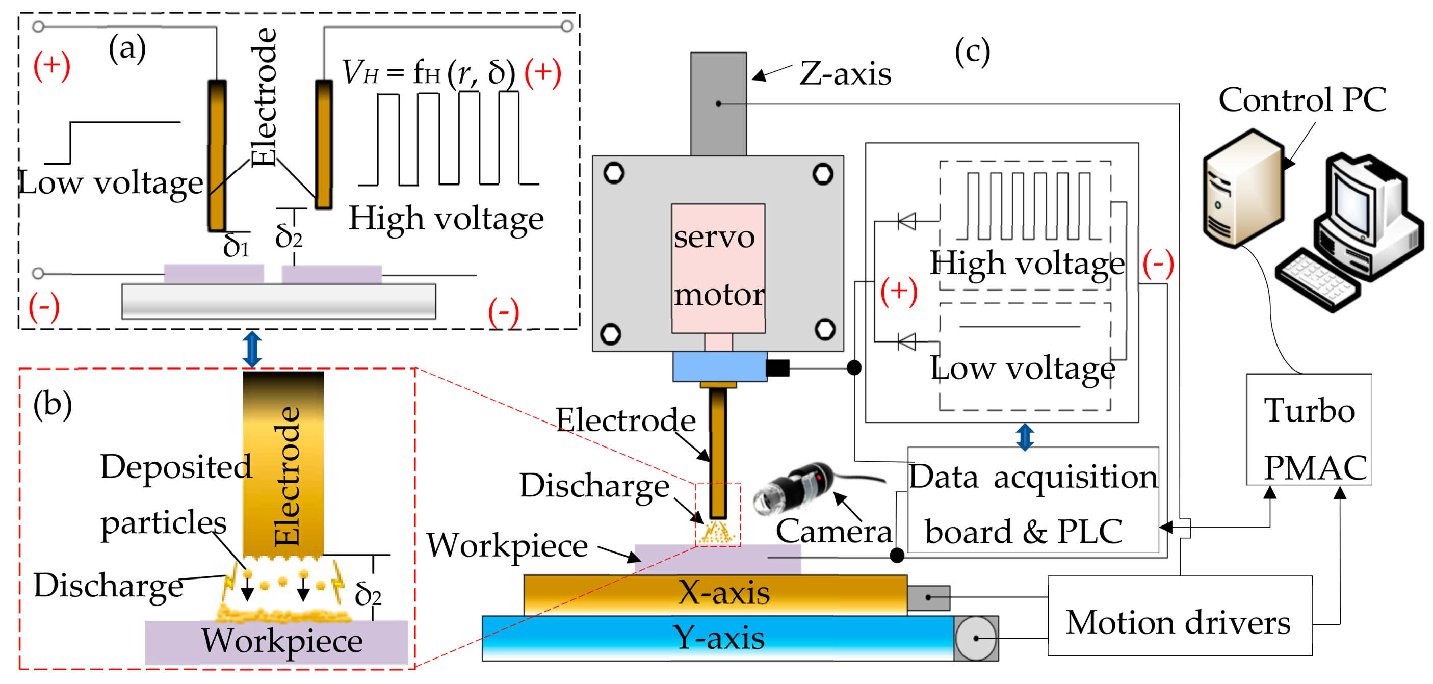
2.2. Principle of HV-μEAM
3. Results and Discussion
3.1. Study on Discharge Process and Deposition Effect
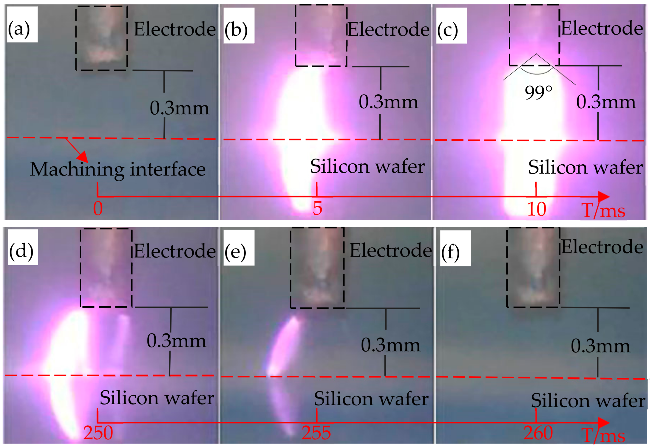
3.1.1. The Discharge Phenomenon of HV
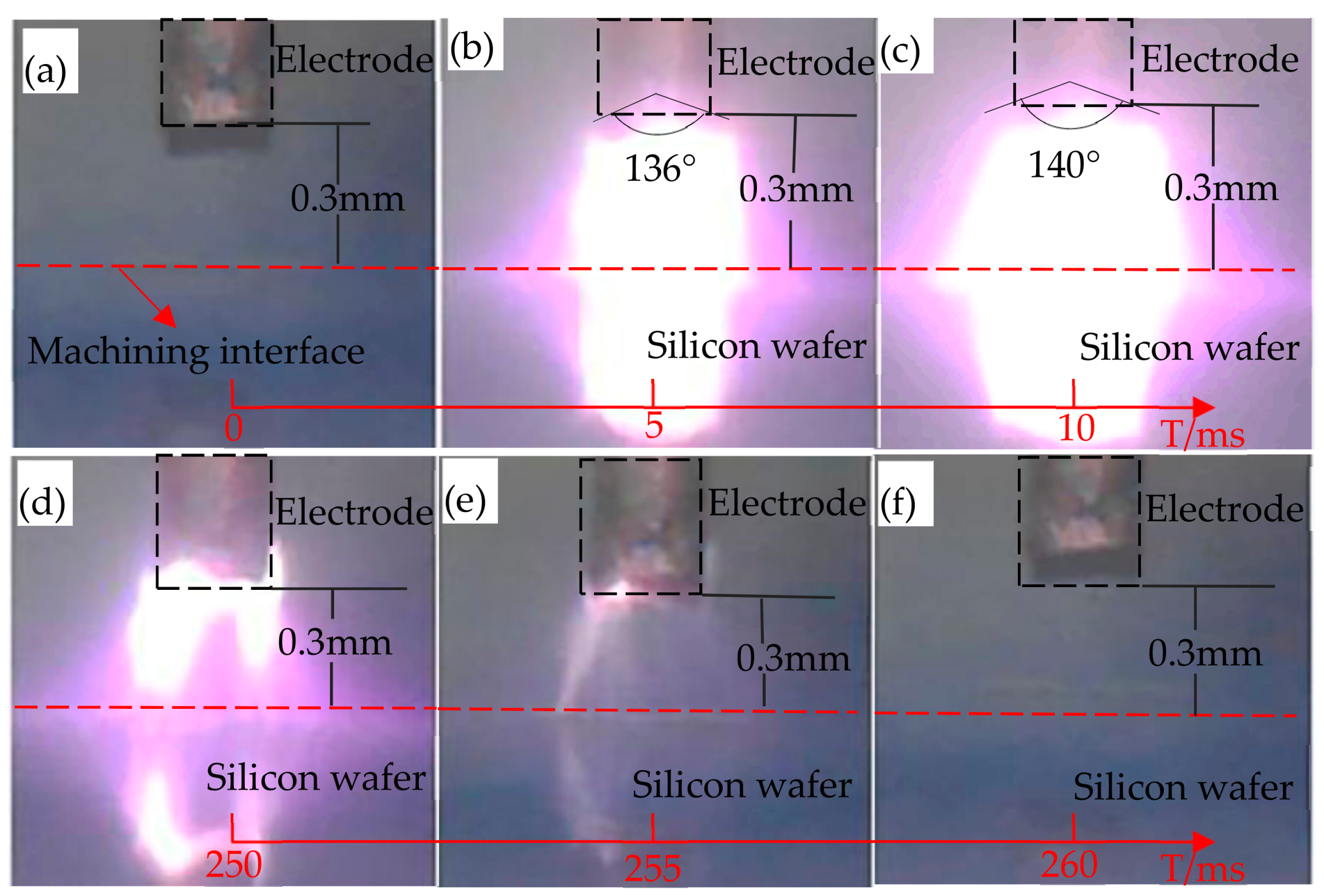
3.1.2. The Discharge Phenomenon of HV-μEAM
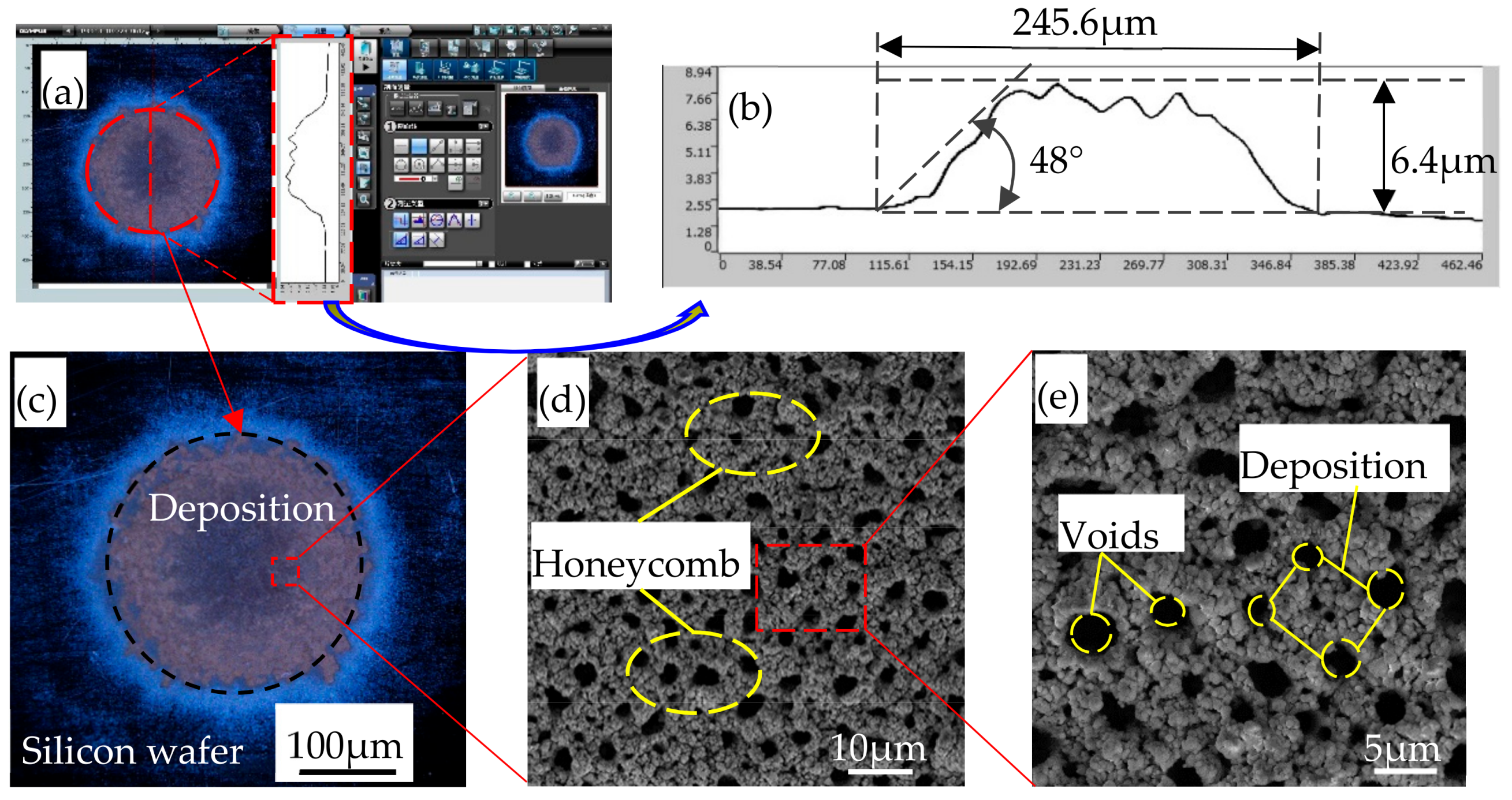
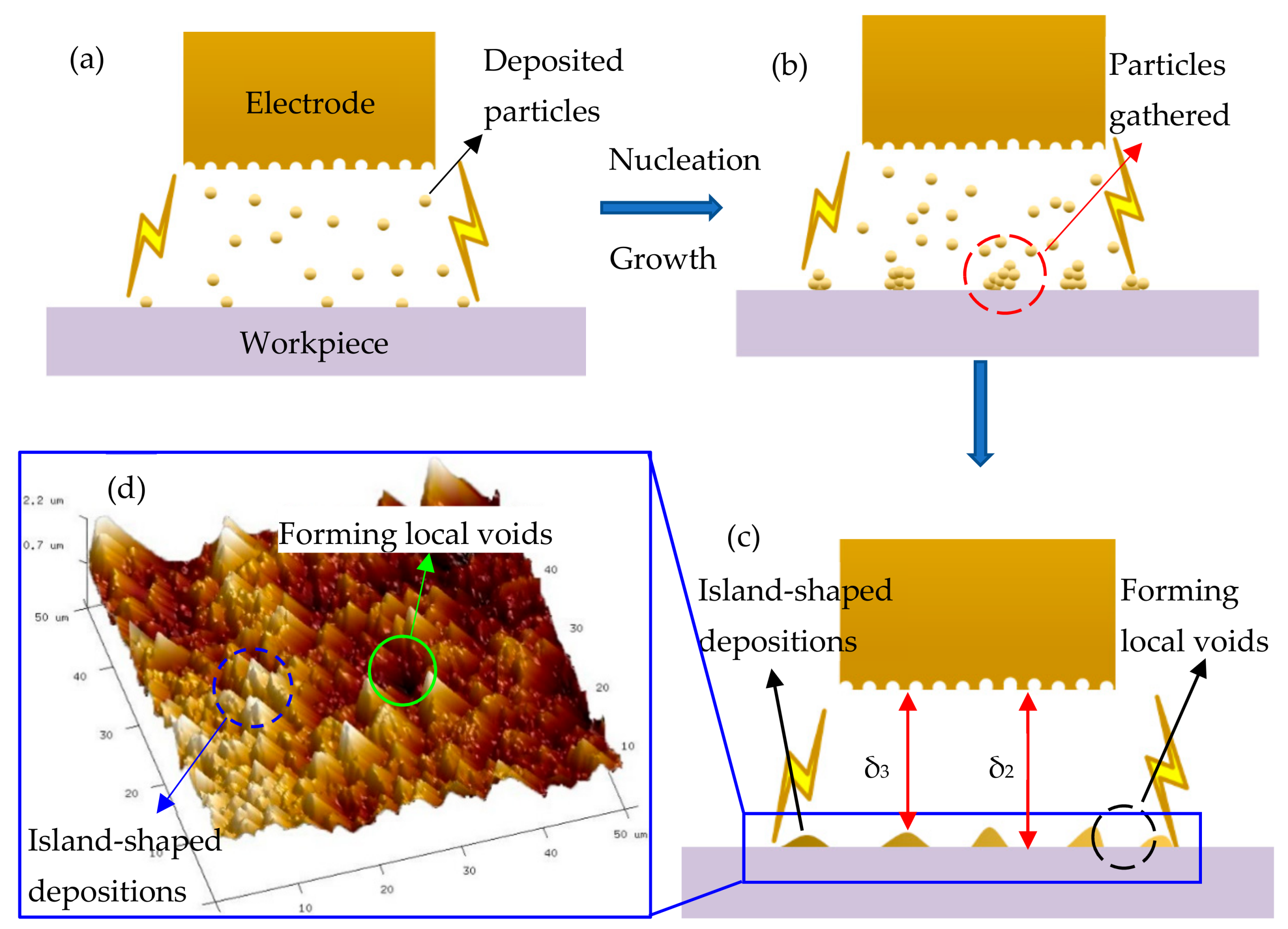
3.1.3. The Deposition Effect
3.1.4. Energy Dispersive Spectroscopy (EDS) Analysis
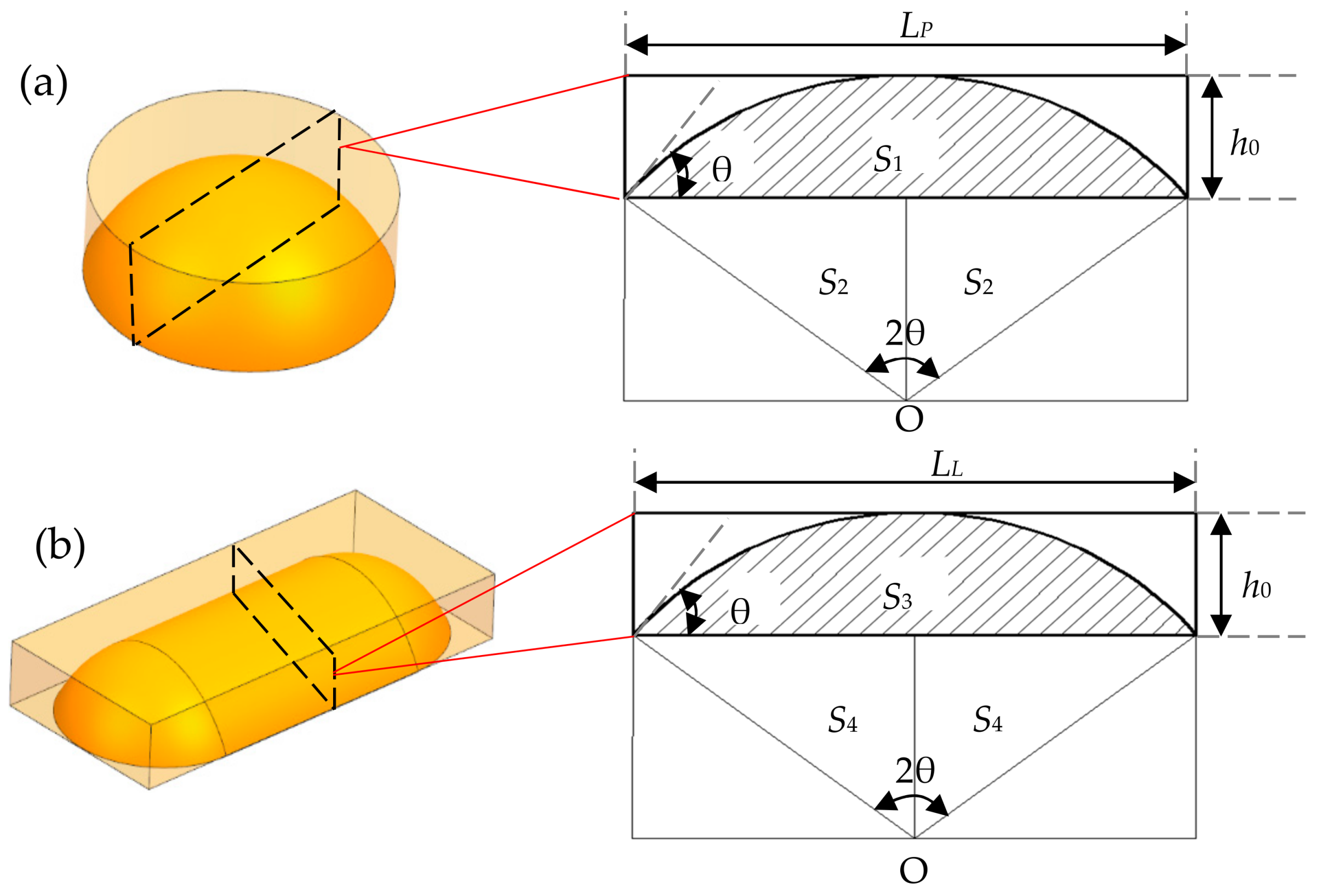
3.1.5. Deposition Models
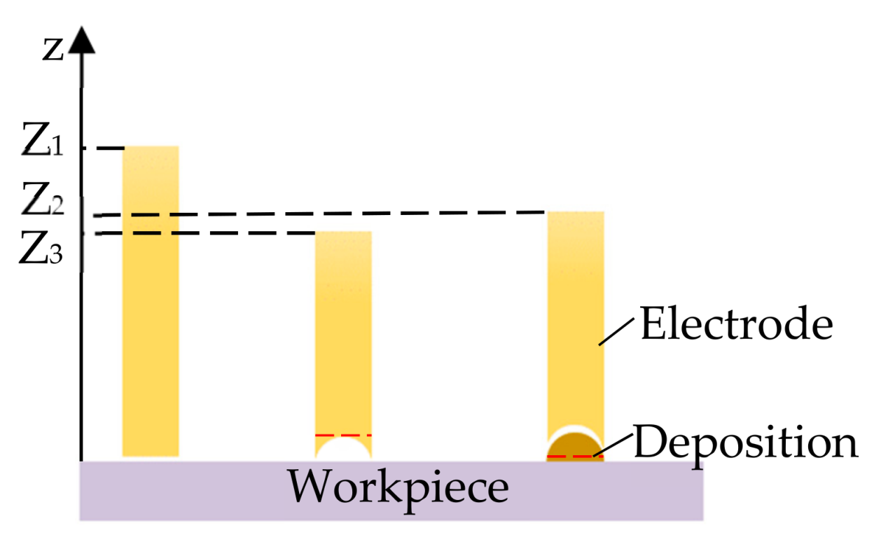
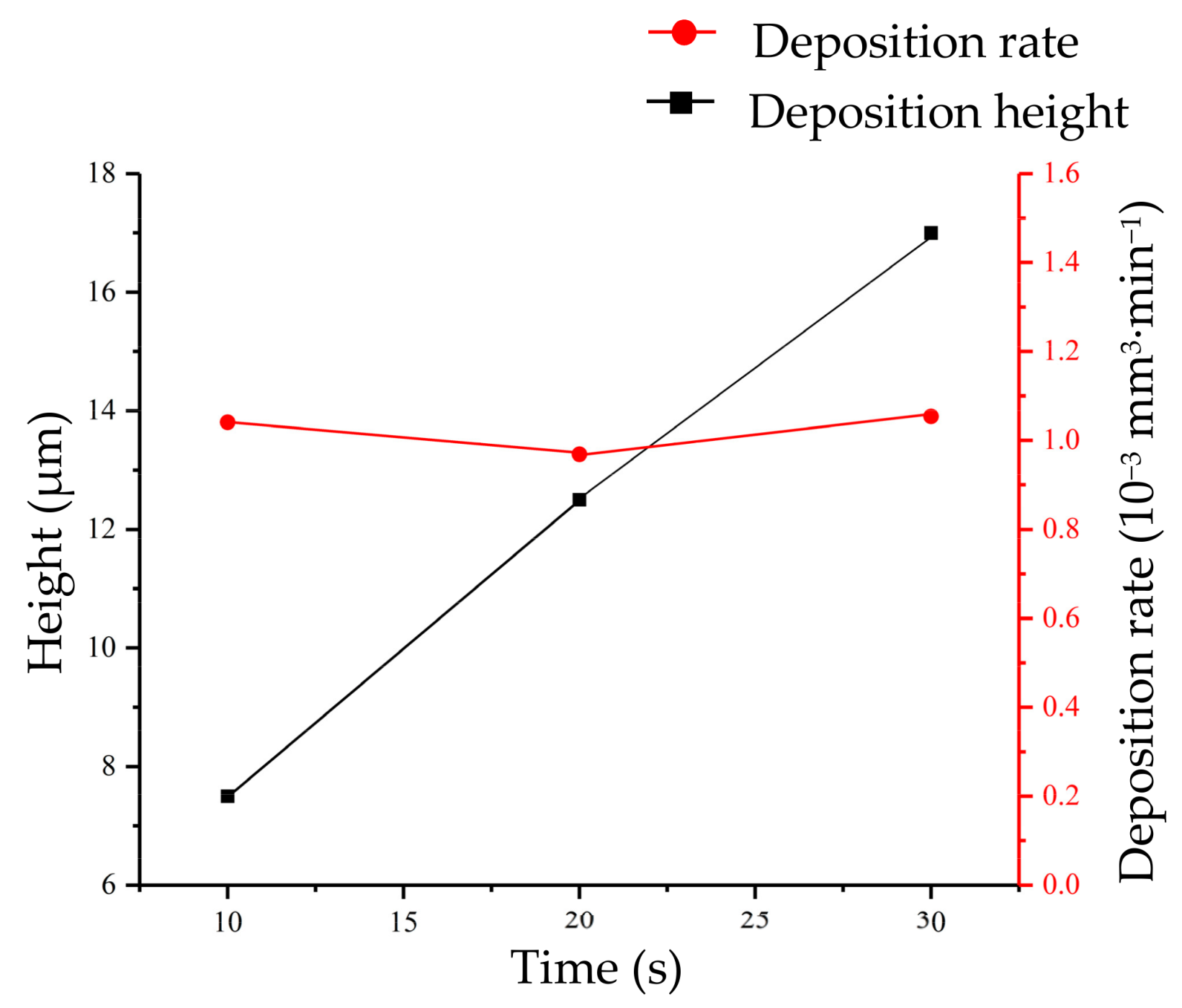
3.1.6. Single Point Multi-Layer Deposition
3.2. Effects of Different Parameters on Deposition
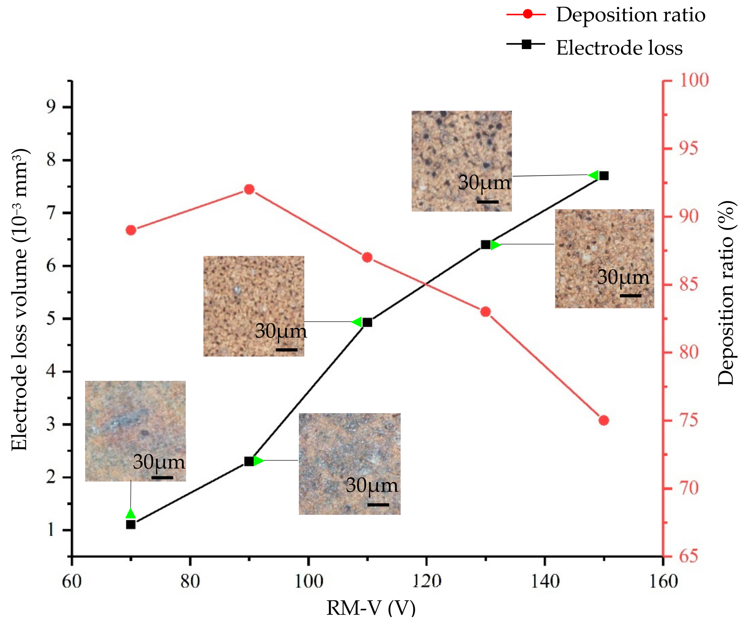
3.2.1. The Effect of RM-V on Deposition
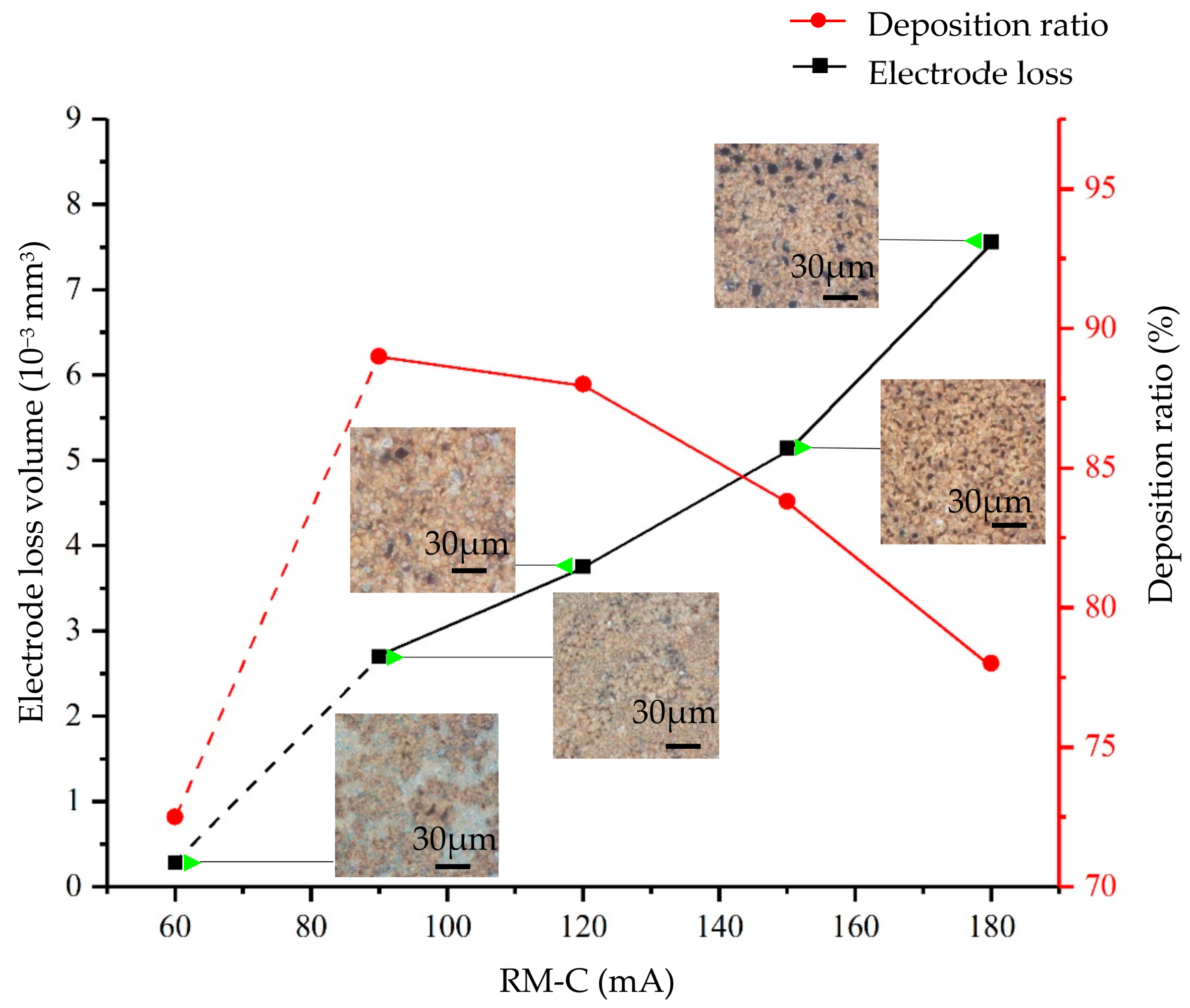
3.2.2. The Effect of RM-C on Deposition
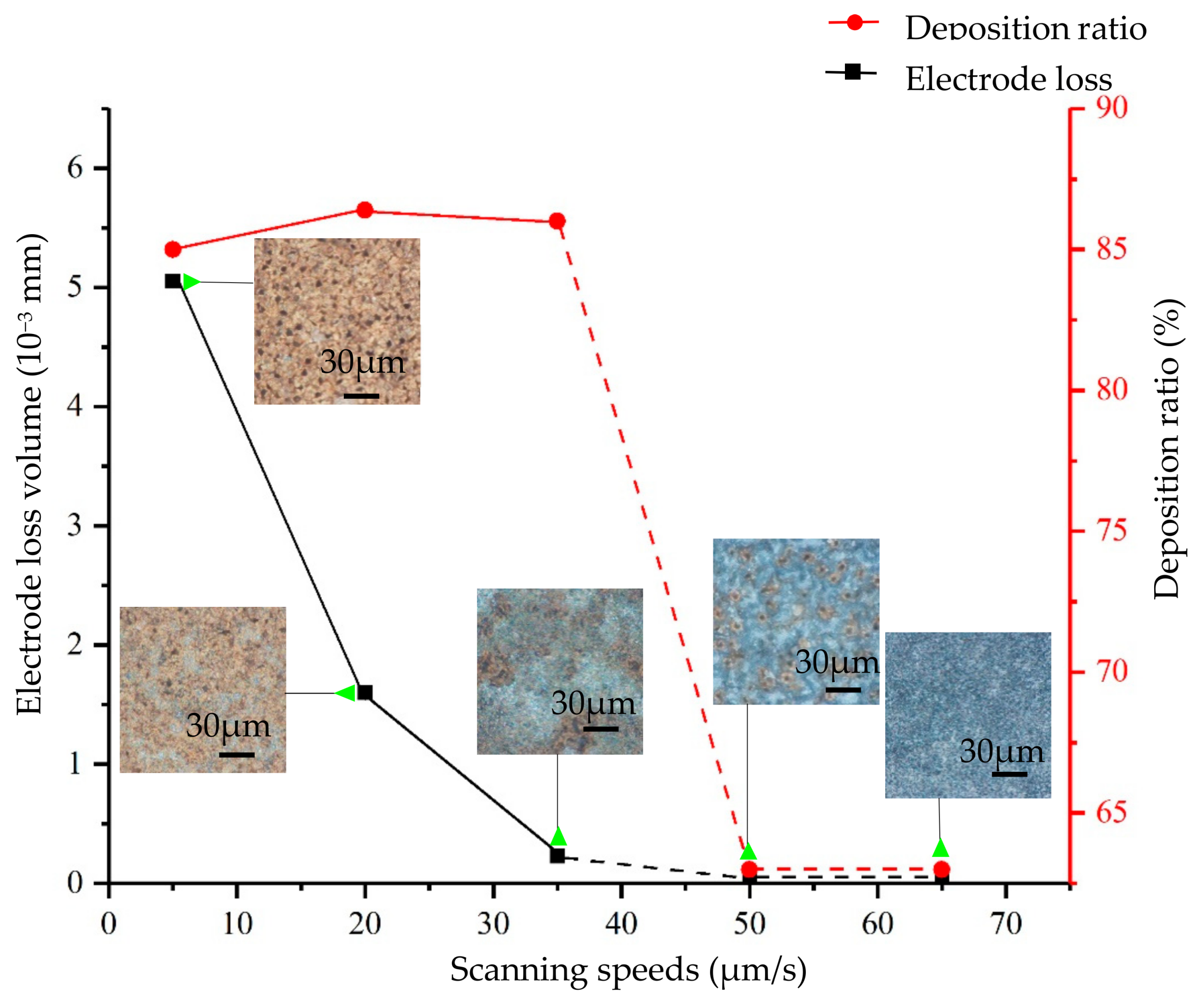
3.2.3. The Effect of Scanning Speed on Deposition
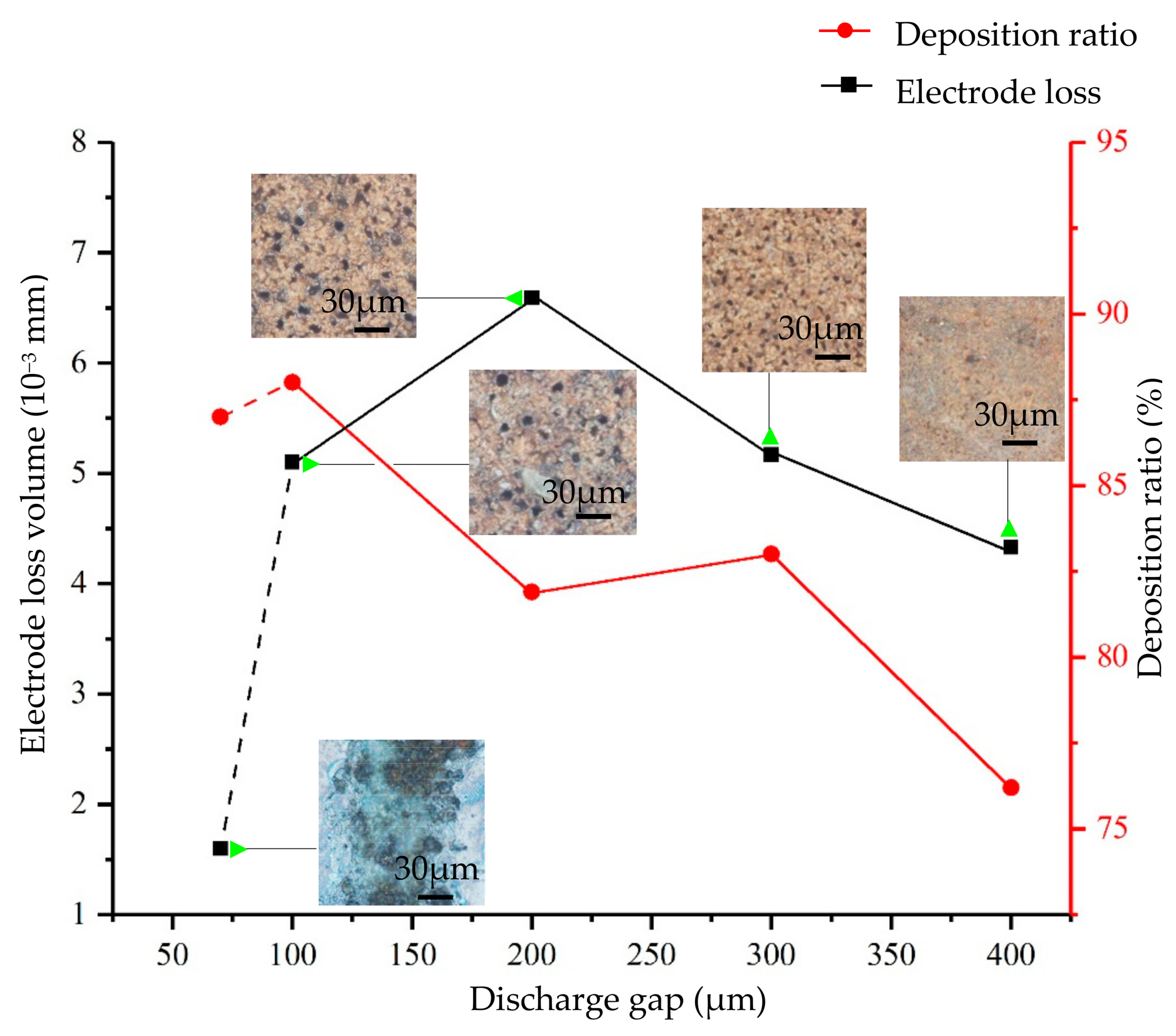
3.2.4. The Effect of Discharge Gap on Deposition
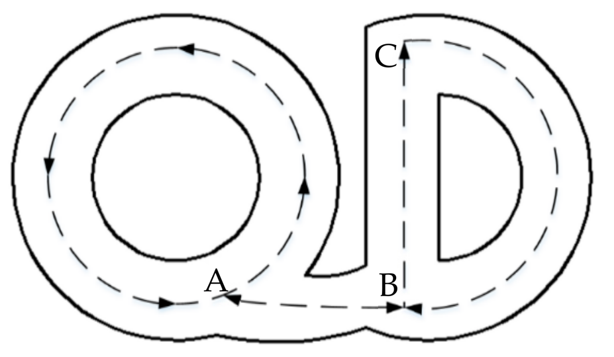
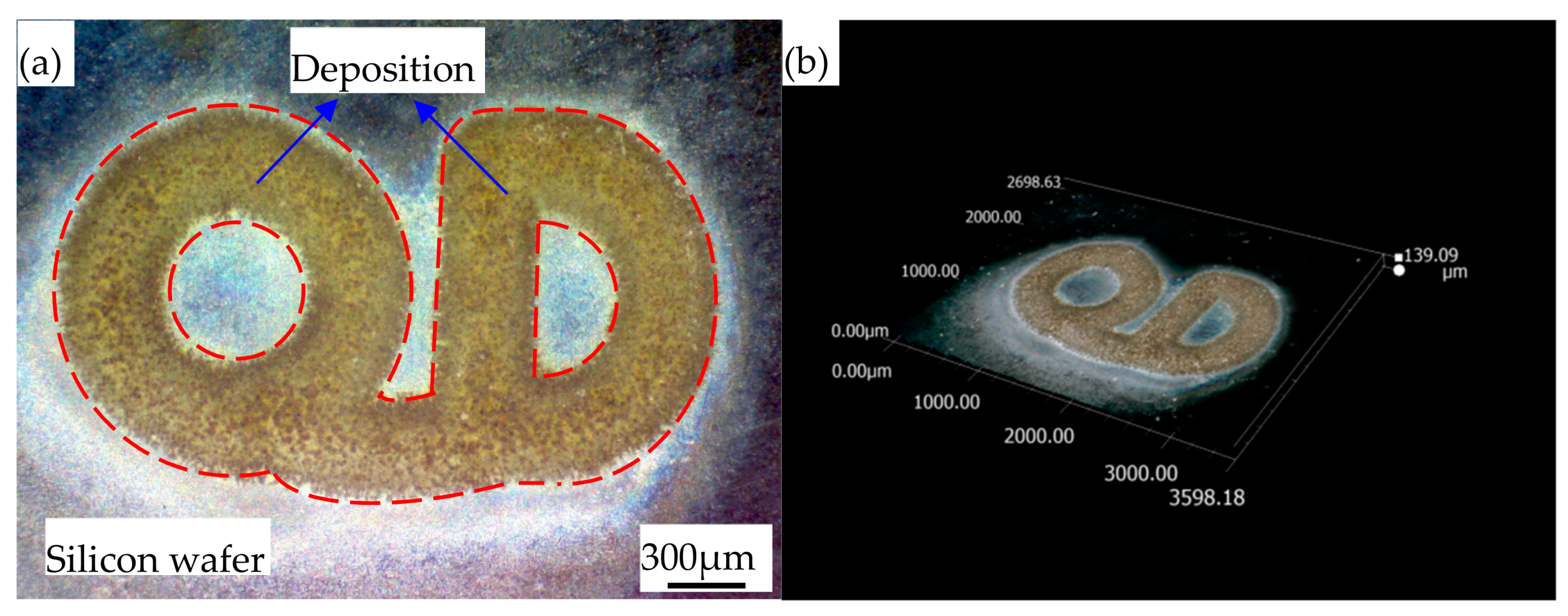
3.3. Deposition Experiment of Complex Trajectory of HV-μEAM
3.3.1. The Experiments of Arc Trajectory
3.3.2. The Experiments of Complex Trajectory
4. Conclusions
- The discharge processes of HV single discharge and HV-μEAM were studied, and the feasibility of HV-μEAM was verified.
- The experiment of HV-μEAM single point on monocrystalline silicon wafer surface was carried out. The effects of various process parameters on the experiment were studied. The optimal process parameters were obtained as follows: RM-V 110 V, RM-C 150 mA, discharge gap 300 μm, scanning speed 5 μm/s.
- Deposition processing of complex trajectory was carried out. The deposition is dense and continuous, the outline is clear and the height is 139.09 μm. The junction between the straight line and the circular arc can achieve a better transition, which proves that this deposition method can achieve the deposition processing of complex tracks on monocrystalline silicon wafer and provides a new choice for realizing the patterning of metallic materials.
Author Contributions
Funding
Conflicts of Interest
References
- Okasha, M.M.; Mativenga, P.T.; Driver, N.; Li, L. Sequential laser and mechanical micro-drilling of Ni superalloy for aerospace application. CIRP Ann. Manuf. Technol. 2010, 59, 199–202. [Google Scholar] [CrossRef]
- Zhou, C.; Yang, Y.; Cai, H.; Ren, T.; Chan, M.; Yang, C. Temperature-compensated high-frequency surface acoustic wave device. IEEE Electron Device Lett. 2013, 34, 1572–1574. [Google Scholar] [CrossRef]
- Li, Y.; Liu, X.; Zhou, Z.; Zhang, L.; Peng, Z. The microstructure and wear resistance of a copper matrix composite layer on copper via nitrogen-shielded arc cladding. Coatings 2016, 6, 67. [Google Scholar] [CrossRef]
- Li, Z.; Bai, J.; Tang, J. Micro-EDM method to fabricate three-dimensional surface textures used as SERS-active substrate. Appl. Surf. Sci. 2018, 458, 810–818. [Google Scholar] [CrossRef]
- Calaon, M.; Islam, A.; Hansen, H.N.; Ravn, C. Experimental investigation of new manufacturing process chains to create micro-metal structures on polymer substrates for lab-on-chip sensors. Int. J. Adv. Manuf. Technol. 2012, 59, 101–109. [Google Scholar] [CrossRef]
- Zhou, W.; Zhang, L.; Ouyang, C.; Wu, J.; Huang, Z.; Xu, X. Micro structural, electrical and optical properties of highly (220) oriented spinel Mn–Co–Ni–O film grown by radio frequency magnetron sputtering. Appl. Surf. Sci. 2014, 311, 443–447. [Google Scholar] [CrossRef]
- Hou, Y.; Huang, Z.; Gao, Y.; Ge, Y.; Wu, J.; Chu, J. Characterization of Mn1.56Co0.96Ni0.48O4 films for infrared detection. Appl. Phys. Lett. 2008, 92, 202115. [Google Scholar] [CrossRef]
- Di, W.; Liu, F.; Lin, T.; Kong, H.; Meng, C.; Zhang, W.; Cheng, Y.; Hou, Y. Influence of oxygen partial pressure on structural and electrical properties of Mn1.56Co0.96Ni0.48O4 thin films deposited by pulsed laser deposition. Appl. Surf. Sci. 2018, 447, 287–291. [Google Scholar] [CrossRef]
- Ahn, C.H.; Allen, M.G. Micromachined planar inductors on silicon wafers for MEMS applications. IEEE Trans. Ind. Electron. 1998, 45, 866–876. [Google Scholar] [CrossRef]
- Jacob, J.; Wahid, R.; Ali, A.; Zahra, R.; Ikram, S.; Amin, N.; Ashfa, A.; Rehman, U.; Rehman, S.; Al-Othmany, D.S.; et al. Growth of Cu2InO4 thin films on Si substrate by thermal evaporation technique and enhancement of thermoelectric properties by post-growth annealing. Phys. B Condens. Matter. 2019, 562, 59–62. [Google Scholar] [CrossRef]
- Ma, C.; Gu, D.; Lin, K.; Dai, D.; Xia, M.; Yang, J.; Wang, H. Selective laser melting additive manufacturing of cancer pagurus’s claw inspired bionic structures with high strength and toughness. Appl. Surf. Sci. 2019, 469, 647–656. [Google Scholar] [CrossRef]
- Alfaify, A.Y.; Hughes, J.; Ridgway, K. Critical evaluation of the pulsed selective laser melting process when fabricating Ti 64 parts using a range of particle size distributions. Addit. Manuf. 2018, 19, 197–204. [Google Scholar] [CrossRef]
- El-Giar, E.M.; Said, R.A.; Bridges, G.E.; Thomson, D.J. Localized electrochemical deposition of copper microstructures. J. Electrochem. Soc. 2000, 147, 586–591. [Google Scholar] [CrossRef]
- Ismail, A.H.; Abdullah, A.H.; Sulaiman, Y. Physical and electrochemical properties of ZnO films fabricated from highly cathodic electrodeposition potentials. Superlattices Microstruct. 2017, 103, 171–179. [Google Scholar] [CrossRef]
- Peng, Z.; Chi, G.; Wang, Z. Micro electrical discharge machining deposition in air for fabrication of micro spiral structures. Chin. J. Mech. Eng. 2010, 23, 154–160. [Google Scholar] [CrossRef]
- Islam, M.M.; Li, C.; Ko, T.J. Dry electrical discharge machining for deburring drilled holes in CFRP composite. Int. J. Precis Eng. Manuf. Green Technol. 2017, 4, 149–154. [Google Scholar] [CrossRef]
- Peng, T.; Chen, C. Influence of energy density on energy demand and porosity of 316L stainless steel fabricated by selective laser melting. Int. J. Precis. Eng. Manuf. Green Technol. 2018, 5, 55–62. [Google Scholar] [CrossRef]
- Zavala-Arredondo, M.; Ali, H.; Groom, K.M.; Mumtaz, K. Investigating the melt pool properties and thermal effects of multi-laser diode area melting. Int. J. Adv. Manuf. Technol. 2018, 97, 1383–1396. [Google Scholar] [CrossRef] [Green Version]
- Lin, J.; Yang, J.; Chang, T.; Jiang, S. On the structure of micrometer copper features fabricated by intermittent micro-anode guided electroplating. Electrochimica Acta 2009, 54, 5703–5708. [Google Scholar] [CrossRef]
- Heinz, J.; Kenneth, G. Fundamental Study of Magnetic Field-Assisted Micro-EDM for Non-Magnetic Materials. Master’s Thesis, University of Illinois at Urbana-Champaign, Champaign, IL, USA, 2010. [Google Scholar]
- Chi, G.; Wang, Z.; Xiao, K.; Cui, J.; Jin, B. The fabrication of a micro-spiral structure using EDM deposition in the air. J. Micromech. Microeng. 2008, 18, 035027. [Google Scholar] [CrossRef]
- Wang, H.; Chi, G.; Wang, Y.; Yu, F.; Wang, Z. Fabrication of superhydrophobic metallic surface on the electrical discharge machining basement. Appl. Surf. Sci. 2019, 478, 110–118. [Google Scholar] [CrossRef]
- Liu, Q.; Zhang, Q.; Wang, K.; Wang, G.; Fu, X.; Zhang, J. Scale effects and a method for similarity evaluation in micro electrical discharge machining. Chin. J. Mech. Eng. 2016, 29, 1193–1199. [Google Scholar] [CrossRef]
- Murray, J.; Zdebski, D.; Clare, A.T. Workpiece debris deposition on tool electrodes and secondary discharge phenomena in micro-EDM. J. Mater. Process. Technol. 2012, 212, 1537–1547. [Google Scholar] [CrossRef]
- Muthuramalingam, T.; Mohan, B. Influence of tool electrode properties on machinability in spark erosion machining. Mater. Manuf. Process. 2013, 28, 939–943. [Google Scholar] [CrossRef]
- Muralidharan, B.; Chelladurai, H.; Singh, P.; Roy, M.K. Single spark analysis of electro-discharge deposition (EDD) process. Mater. Manuf. Process. 2015, 31, 1853–1864. [Google Scholar] [CrossRef]
- Chen, S.; Chen, C. Development of a novel micro w-EDM power source with a multiple Resistor-Capacitor (mRC) relaxation circuit for machining high-melting point, -hardness and -resistance materials. J. Mater. Process. Technol. 2017, 240, 370–381. [Google Scholar] [CrossRef]
- Feng, W.; Chu, X.; Hong, Y.; Zhang, L. Studies on the surface of high-performance alloys machined by micro-EDM. Mater. Manuf. Process. 2017, 33, 616–625. [Google Scholar] [CrossRef]
- Macedo, F.T.B.; Wiessner, M.; Hollenstein, C.; Martendal, C.P.; Kuster, F.; Wegener, K. Anode power deposition in dry EDM. Int. J. Precis. Eng. Manuf. Green Technol. 2019, 6, 197–210. [Google Scholar] [CrossRef]
- Yue, X.; Yang, X.; Masanori, K. Influence of metal vapor jets from tool electrode on material removal of workpiece in EDM. Prec. Eng. 2018, 53, 278–288. [Google Scholar] [CrossRef]
- Jain, V.K.; Seshank, S.; Sidpara, A.; Jain, H. Some aspects of micro-fabrication using electro discharge deposition process. In Proceedings of the ASME/ISCIE 2012 International Symposium on Flexible Automation, St. Louis, MI, USA, 8–20 June 2012; pp. 419–424. [Google Scholar]
- Muralidharan, B.; Chelladurai, H. Experimental analysis of electro-discharge deposition process. Int. J. Adv. Manuf. Technol. 2015, 76, 69–82. [Google Scholar] [CrossRef]
- Gu, L.; Zhu, Y.; He, G.; Farhadi, A.; Zhao, W. Coupled numerical simulation of arc plasma channel evolution and discharge crater formation in arc discharge machining. Int. J. Heat Mass. Transf. 2019, 135, 674–684. [Google Scholar] [CrossRef]
- Zhang, R.; Zhang, Y.; Liu, Y.; Shen, Y.; Li, Z.; Wang, X. Energy distribution and material removal of electric arc machining (EAM). J. Mater. Process. Tech. 2017, 242, 110–116. [Google Scholar] [CrossRef]
- Ahmed, A.; Fardin, A.; Tanjilul, M.; Wong, Y.S.; Rahman, M.; Kumar, A.S. A comparative study on the modelling of EDM and hybrid electrical discharge and arc machining considering latent heat and temperature-dependent properties of Inconel 718. Int. J. Adv. Manuf. Technol. 2018, 94, 2729–2737. [Google Scholar] [CrossRef]
- Zhu, G.; Zhang, Q.; Wang, H.; Wang, K.; Zhang, M. Machining behaviors of short electrical arc milling with high frequency and high voltage pulses. Int. J. Adv. Manuf. Technol. 2017, 90, 1067–1074. [Google Scholar] [CrossRef]
- Li, Y.; Zhang, S.; Peng, Z.; Guo, F. A study on the mechanism of crystal cracking in GTA welding of copper plates. Mater. Manuf. Process. 2016, 31, 2143–2151. [Google Scholar]
- Zhu, Y.; Gu, L.; Farhadi, A.; He, G.; Zhao, W. Observation and analyzation of plasma channel evolution behavior in air flushing electrical arc machining. Int. J. Adv. Manuf. Technol. 2019, 100, 3127–3138. [Google Scholar] [CrossRef]
- Hayakawa, N.; Yoshitake, Y.; Koshino, N.; Ueda, T.; Okubo, H. Impulse partial discharge characteristics and their mechanisms under non-uniform electric field in N2/SF6 gas mixtures. IEEE Trns. Dielectr. Electr. Insul. 2005, 12, 1035–1042. [Google Scholar] [CrossRef]
- Bogaerts, A.; Neyts, E.; Gijbels, R.; Mullen, J.V.D. Gas discharge plasmas and their applications. Spectrochimica Acta Part B. 2002, 57, 609–658. [Google Scholar] [CrossRef]
- Maruvada, P.S.; Menemenlis, H.; Malewski, R. Corona characteristics of conductor bundles under impulse voltages. IEEE Trans. Power App. Syst. 1977, 96, 102–115. [Google Scholar] [CrossRef]
- Xu, M.; Tan, Z.; Li, K. Modified peek formula for calculating positive DC Corona inception electric field under variable humidity. IEEE Trns. Dielectr. Electr. Insul. 2019, 19, 1377–1382. [Google Scholar] [CrossRef]
- Spyrou, N.; Peyrous, R.; Soulem, N.; Held, B. Why Paschen’s law does not apply in low-pressure gas discharges with inhomogeneous fields. J. Phys. D Appl. Phys. 1995, 28, 701–710. [Google Scholar] [CrossRef]
- Subramanian, R.; Natarajan, B.; Kaliyaperumal, B.; Chinnasamy, R. Effect of MIG welding process parameters on microstructure and tensile behavior of hastelloy C276 using response surface methodology. Mater. Res. Express. 2019, 6, 066540. [Google Scholar] [CrossRef]


| Parameters | Value |
|---|---|
| Voltage (V) | 2000 |
| Current (mA) | 0.3 |
| Discharge gap (μm) | 300 |
| Parameters | Value |
|---|---|
| HV (V) | 2000 |
| Current of HV (mA) | 0.3 |
| RM-V (V) | 110 |
| RM-C (mA) | 150 |
| Discharge gap (μm) | 300 |
| Parameters | Value |
|---|---|
| HV (V) | 2000 |
| Current of HV (mA) | 0.3 |
| RM-V (V) | 110 |
| RM-C (mA) | 150 |
| Discharge gap (μm) | 300 |
| Parameters | Value |
|---|---|
| HV (V) | 2000 |
| Current of HV (mA) | 0.3 |
| RM-V (V) | 70, 90, 110, 130, 150 |
| RM-C (mA) | 60, 90, 120, 150, 180 |
| Discharge gap (μm) | 70, 100, 200, 300, 400 |
| Scanning speed (μm/s) | 5, 20, 35, 50, 65 |
| Scanning distance (mm) | 1 |
| Parameters | Value |
|---|---|
| HV (V) | 2000 |
| Current of HV (mA) | 0.3 |
| RM-V (V) | 110 |
| RM-C (mA) | 150 |
| Discharge gap (μm) | 300 |
| Scanning speed (μm/s) | 5 |
© 2019 by the authors. Licensee MDPI, Basel, Switzerland. This article is an open access article distributed under the terms and conditions of the Creative Commons Attribution (CC BY) license (http://creativecommons.org/licenses/by/4.0/).
Share and Cite
Peng, Z.; Feng, T.; Wei, Z.; Zhang, Y.; Li, Y. Directly Writing Patterning of Conductive Material by High Voltage Induced Weak Electric Arc Machining (HV-μEAM). Coatings 2019, 9, 538. https://doi.org/10.3390/coatings9090538
Peng Z, Feng T, Wei Z, Zhang Y, Li Y. Directly Writing Patterning of Conductive Material by High Voltage Induced Weak Electric Arc Machining (HV-μEAM). Coatings. 2019; 9(9):538. https://doi.org/10.3390/coatings9090538
Chicago/Turabian StylePeng, Zilong, Tianming Feng, Zilong Wei, Yong Zhang, and Yinan Li. 2019. "Directly Writing Patterning of Conductive Material by High Voltage Induced Weak Electric Arc Machining (HV-μEAM)" Coatings 9, no. 9: 538. https://doi.org/10.3390/coatings9090538
APA StylePeng, Z., Feng, T., Wei, Z., Zhang, Y., & Li, Y. (2019). Directly Writing Patterning of Conductive Material by High Voltage Induced Weak Electric Arc Machining (HV-μEAM). Coatings, 9(9), 538. https://doi.org/10.3390/coatings9090538