1. Introduction
Hard metal is the most widely used substrate material for diamond coated tools. The interaction between the deposition temperature and the methane concentration needs to be known to be able to find the best processing conditions for the chemical vapour deposition (CVD) of diamond coatings, according to the desired coating thickness, deposition duration, and the medium diamond crystal size. According to Song et al. [
1], the dependence of the deposition temperature on the diamond deposition is still of current interest.
Without sample pre-treatment of hard metal substrates, the catalysing effect of cobalt occurs during the process [
2]. The absorption of atomic carbon thus results in delayed diamond nucleation. In addition, cooling of the substrate reduces the solubility of carbon in cobalt, and an amorphous carbon phase and graphite are released. This reduces the adhesive strength of the overlying diamond layer [
2]. Haubner et al. [
3] published that carbon starts to diffuse in hard metals at 800 °C and the amounts of tungsten and carbon, which are dissolved in the cobalt binder, increase with rising temperatures and start to change at approximately 1000 °C.
Increasing the filament temperature in hot-filament CVD (HF-CVD) processes leads to rising concentrations of CH
3 [
4]. Increasing the filament substrate distance, as well as lowering the deposition temperatures lead to decreasing CH
3-concentration due to the recombination of CH
3 to CH
4 or C
2H
6 [
4]. A rising filament temperature in an HF-CVD process at constant deposition temperature leads to an increasing diamond film thickness [
5]. An increasing methane concentration also leads to an increasing diamond film thickness, whereby the critical methane concentration is dependent on the filament temperature. The critical methane concentration at the filament temperature of 2000 °C is 1% CH
4 and rises in the case of a temperature of 2600 °C to 6% CH
4. Weng et al. [
6] investigated the process window of a microwave plasma CVD process by deposition at three different deposition temperatures (780 to 940 °C) and methane concentrations (0.8% to 4.0%) and concluded that the quality of the diamond films increases with increasing deposition temperature.
The working hypothesis of this study is that a wider range of methane concentrations could be used to deposit microcrystalline diamond coatings due to the increasing etching and deposition rate with rising deposition temperatures. Seventy-two different coatings were deposited to prove the hypothesis.
2. Materials and Methods
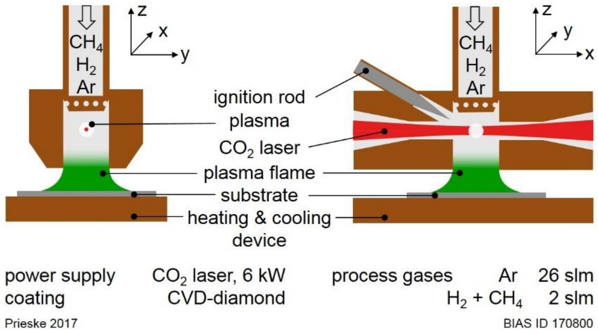
A laser-based plasma (LaPlas) CVD process was used at atmospheric pressure without a vacuum chamber to deposit polycrystalline CVD diamond coatings [
7]. The schematic layout of the LaPlas CVD process is shown in
Figure 1. A 6 kW high power CO
2 laser (Trumpf TLF 6000, Ditzingen, Germany) with the wavelength of 10.6 µm is utilised as an energy supply of an argon plasma jet. The ignition of the plasma flame is achieved by inserting a tungsten lanthanum electrode into the laser focus. After the ignition of the argon plasma flame (26 standard litres per min (slm) Argon), the process gases methane and hydrogen, which are required for CVD synthesis of polycrystalline diamond, are introduced. The summed gas flow of methane and hydrogen was set to 2.0 slm. The methane concentration was varied from 0.15% up to 5.0% regarding the total gas flow of hydrogen and methane.
As substrate material, K10 hard metal discs with a diameter of 20.3 mm and a thickness of 3.0 ± 0.15 mm were used, consisting of 94% tungsten carbide and 6% cobalt. The substrates where etched by Murakami reagent (K
3Fe(CN)
6:KOH:H
2O = 1:1:10) for 30 min and subsequently with Caro’s reagent (3 mL 96 wt % H
2SO
4, 88 mL 40%
w/
v H
2O
2) for one minute [
8]. The diamond nucleation was carried out with a dispersion of 200 mL isopropanol and 210 mg diamond powder with the average crystal size in the range of 0.25 μm to 0.50 μm from the company Microdiamant AG (Lengwil, Switzerland). The substrates were put into the dispersion within an ultrasonic bath for ten minutes and subsequently into isopropanol for three minutes.
Three pyrometers were used for temperature monitoring: IMPAC (Frankfurt, Germany) pyrometer IGAR 12 LO, IP 140 and IGA 10. The K10 hard metal substrate was heated up exemplarily to 800 °C, which was measured by a thermocouple, to determine the emission coefficient for each pyrometer. The emission coefficients were set to 0.98 for the pyrometer IGAR 12 LO and IP 140 and to 0.86 for pyrometer IGA 10. A feedback control was implemented, which regulates the laser power according to the substrate temperature measured by the IMPAC pyrometer IGAR 12 LO to ensure a constant deposition temperature over the deposition time of 20 min. Detailed information about the implementation of the feedback control is published in [
9]. The measuring accuracy was ±10 K due to the remaining inaccuracies of the determined emission coefficients and the feedback control.
To characterise the process window for the deposition of diamond coatings with the LaPlas CVD process, 72 different deposition parameter sets were applied for process temperatures from 650 to 1100 °C and methane concentrations from 0.15% to 5.0%. The temperature was increased in 50 K steps.
Scanning electron microscopy (SEM) (Carl Zeiss Microscopy EVO MA-10, Oberkochen, Germany) and 3D laser scanning confocal microscopy (Keyence VK 9710, Osaka, Japan) were used to take images of the coating surfaces and measure the coating thicknesses, as well as the average crystal sizes. An energy dispersive X-ray spectroscopy (EDX) (Bruker Nano GmbH XFlash Detector 610M, Billerica, MA, USA) integrated into the SEM was applied for element analyses and mapping measurements. Micro-Raman spectroscopy (Renishaw system 1000, Wotton-under-Edge, UK) enabled the detection of diamond and graphite by using the excitation wavelength of 514 nm. The existence of diamond was proofed by the measurement of the first order Raman line of the diamond at 1332 cm
−1 [
10]. The G-band at 1560 cm
−1 [
11] in the Raman spectra, was utilized to detect graphite in the deposited coatings. Equation (1) [
12,
13] was used to calculate the diamond quality factors
Q of the deposited coatings using the peak intensity of the diamond Raman line
ID and the intensity of the G-band peak
IG. The diamond quality factor allows for a semi-quantitative estimate of the quality of a diamond coating, i.e., the concentration of the sp
3-bonds compared to sp
2-bonds.
Cryofractures were prepared to accurately determine the coating thickness. A slit was eroded in the backside of the sample up to 500 µm below the surface by electrical discharge machining. Afterwards, the specimens were cooled down by liquid nitrogen and cryofractures were carried out.
3. Results
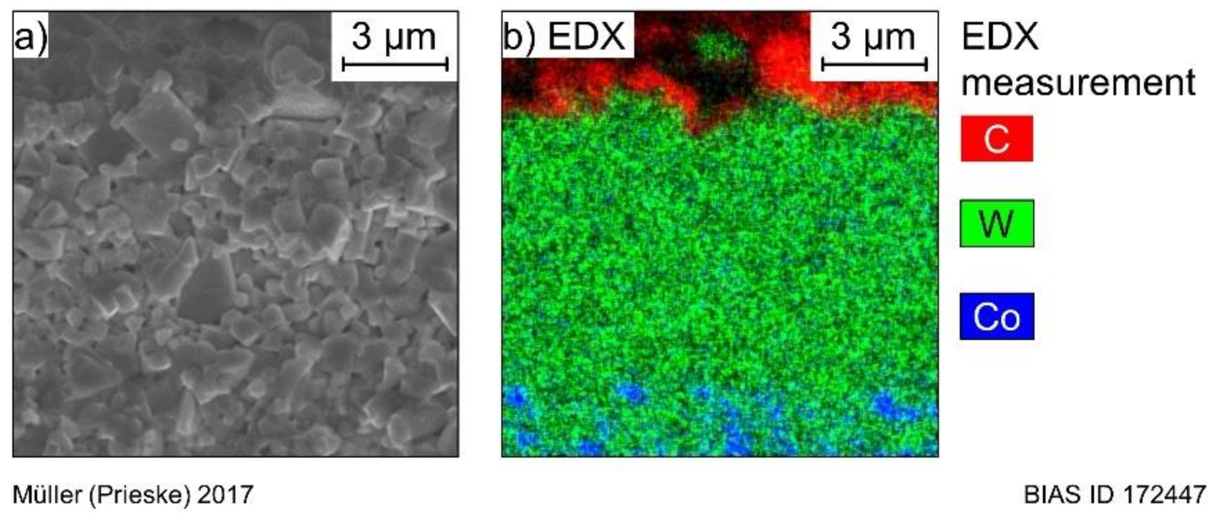
EDX measurements on the pretreated substrates were made to assure that the cobalt binder was completely etched from the surface of the substrate. The measurements showed a cobalt content of 0% on the surface. Furthermore, EDX mappings were done on the cryofractured surface of another sample coated with diamond deposited at 850 °C. An exemplary mapping is depicted in
Figure 2, which shows that cobalt is removed roughly 9 µm deep into the substrate. Hence, the diamond coating was deposited without the influence of the cobalt binder.
In
Figure 3, the investigated process window for the polycrystalline diamond deposition onto hard metal is shown by illustrating the corresponding crystal sizes by the marked size. The results show that coatings are deposited in the examined temperature range from 650 to 1100 °C. A methane concentration of 0.15% is too low for achieving a deposition in case of all process temperatures carried out. For methane concentrations of 0.25% and 0.5%, depositions were achieved up to 800 and 1000 °C, respectively. For methane concentrations from 1.0% to 5%, all investigated temperatures result in coating depositions. With increasing process temperature, the crystal sizes firstly increase before they decrease again with further increasing temperature. In addition, the crystal sizes firstly increase with increasing methane concentration before they also again decrease for further increasing methane concentration.
For samples produced with methane concentrations below the process window, stated by “no growth” in
Figure 3, the Raman measurements showed no peak in the recorded spectrum, as can be seen in
Figure 4a for a coating deposited at 1050 °C and a methane concentration of 0.5%. In case of concentrations in the middle of the process window, the coatings show a clear diamond peak in the Raman spectrum, as is seen exemplarily in
Figure 4b for a coating deposited at 1050 °C and the methane concentration of 2.0%. Here a diamond quality factor of 0.85% or 85% was reached. The Raman spectrum of the coatings shows an increasing G-band graphite peak while only a small diamond peak is formed when the methane concentrations are high and therefore close to the right-hand side of the investigated process window. This is seen in
Figure 4c for a coating deposited at 1050 °C and the methane concentration of 5%. The diamond quality factor of this coating is determined to be 0.62% or 62%.
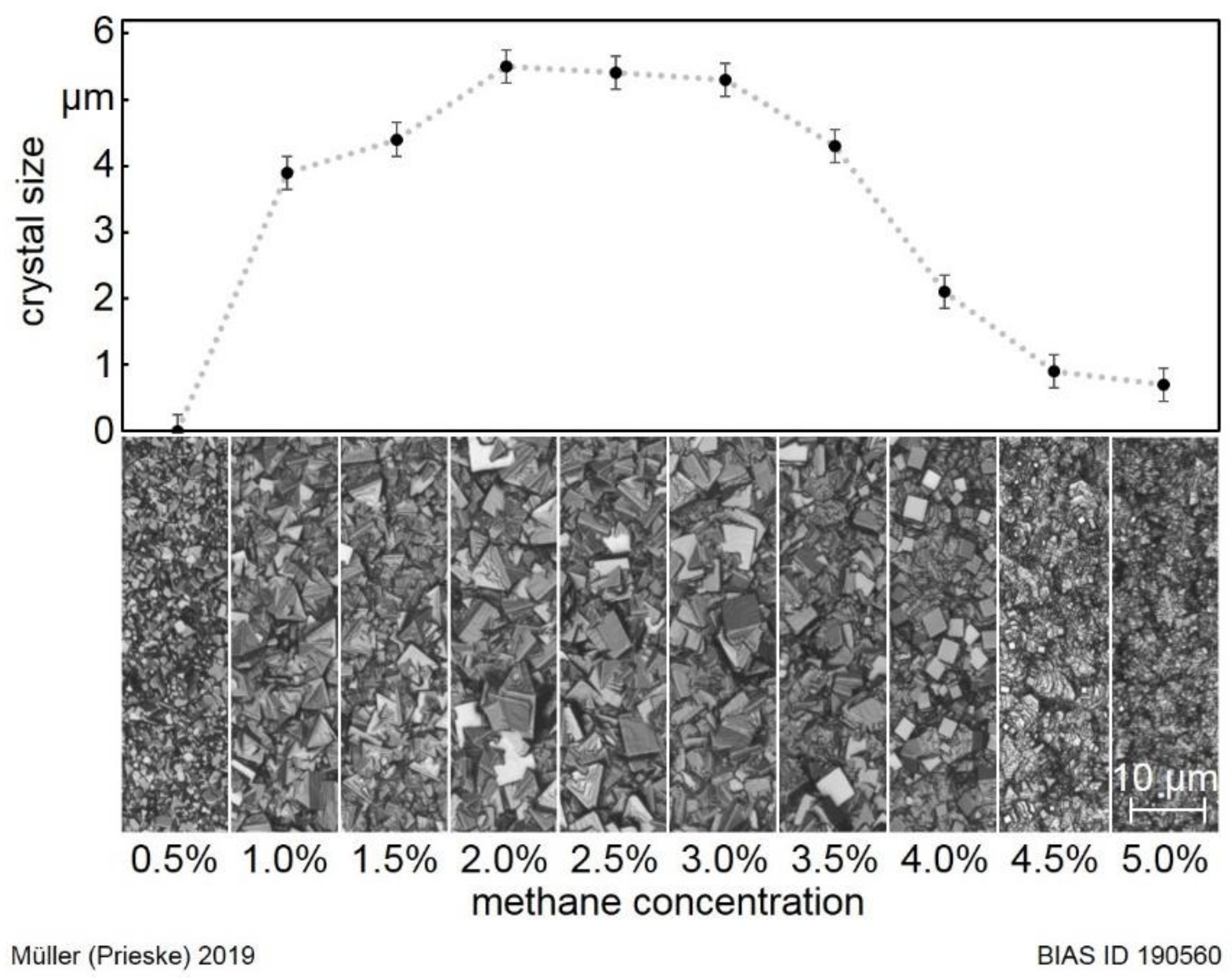
The average crystal sizes of the coatings deposited at the temperature of 1050 °C were measured. The determined values are given in
Figure 5 as a function of the methane concentration. For the methane concentration of 0.5%, no coating is deposited. The tungsten carbide substrate surface is still visible after the process. For increasing concentrations up to 2.0%, the crystal size also increases up to 5.5 µm. Until the concentration of 3.0% is reached, the crystal size decreases slightly to around 5.3 µm. In the case of higher methane concentrations, the crystal size decreases to less than 1 µm at 5.0% methane.
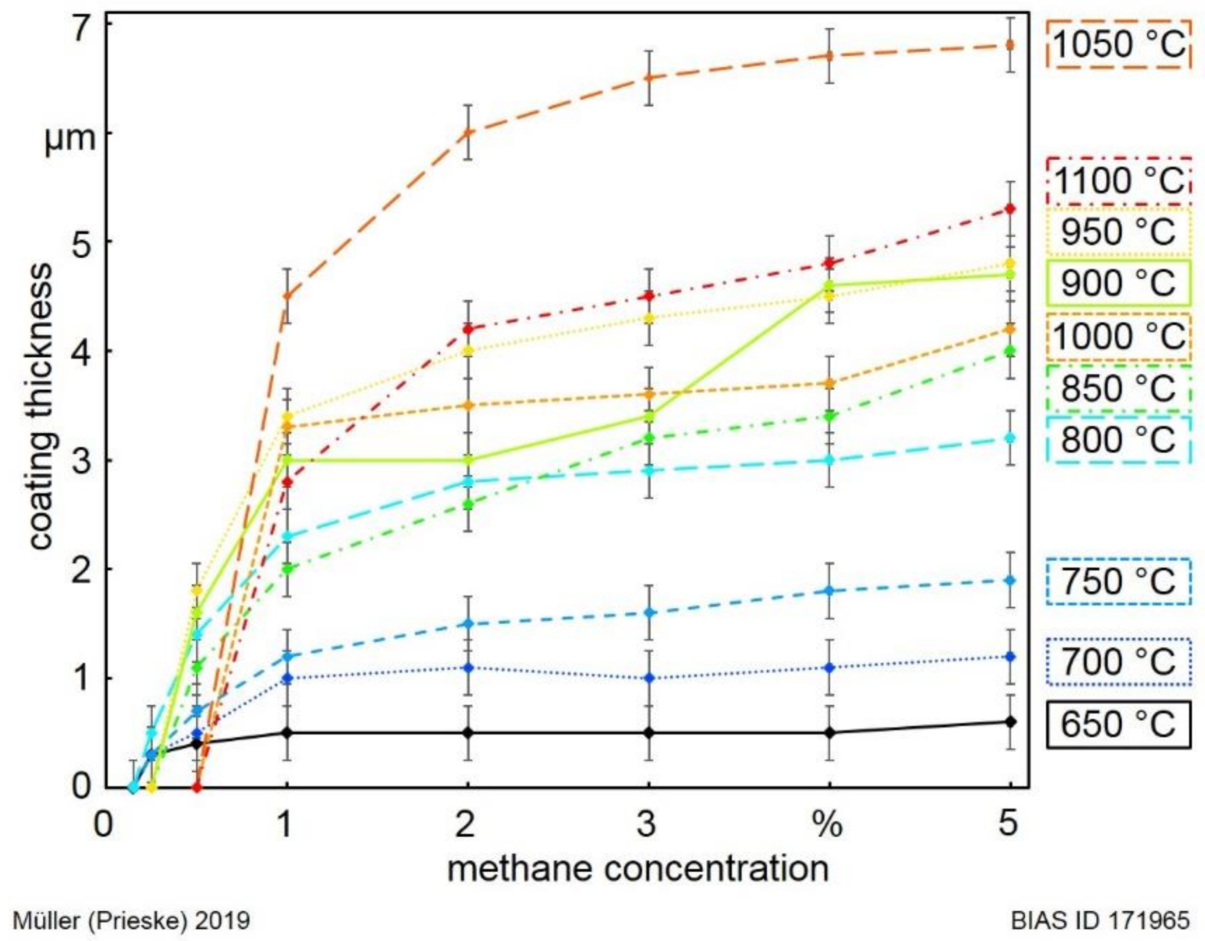
The coating thickness of the samples, synthesised with the deposition time of 20 min, was measured by using cryofractures. The coating thickness as a function of the methane concentration, is given in
Figure 6 for different process temperatures. For increasing methane concentrations and deposition temperatures, the coating thickness increases. However, the coating thickness saturates for increasing methane concentrations at each temperature. In contrast to the visible tendency in the relation between temperature and coating thickness, the process temperature of 1050 °C corresponds to the thickest coating on the hard metal substrates. The coatings deposited at the process temperature of 1100 °C are clearly thinner in comparison to the 1050 °C samples. In the case of the temperature of 1050 °C and the methane concentration of 3.0% (middle of the process window), the coating thickness of 6.5 µm was reached after 20 min of deposition. A microcrystalline diamond coating was deposited (see
Figure 5). The diamond coating deposited at the methane concentration of 5.0% and the deposition temperature of 1050 °C reaches a coating thickness of 6.8 µm even though the crystal size is smaller than one micrometre (see
Figure 5).
In order to check whether the unexpected behaviour of the coatings deposited at 1100 °C is due to an onset of cobalt diffusions, an EDX mapping was performed, which is given in
Figure 7. At the process temperature of 1050 °C, the EDX mapping (
Figure 7b) shows a relatively clear limit of the cobalt binder removal by the etching process and that cobalt had not diffused to the surfaces of the substrate after the coating process. This clear boundary is no longer present after a coating process at 1100 °C (
Figure 7a).
Coatings with different deposition times were produced to find out if a coating thickness could be converted directly into a growth rate. In
Figure 8, the coating thickness is depicted as a function of the deposition time. After the deposition time of 2.5 min, a thin coating could be seen. EDX measurements show 96% carbon content on the surface. An optically closed 1.3 µm thick coating was deposited when increasing the deposition time to five minutes. The measured carbon content of the surface for this coating is 98%. A further increase of the deposition time results in a linear increase of the coating thickness. Therefore, the data given in
Figure 8a was used to determine the constant growth rate of 22 µm/h.
4. Discussion
The results are based on pre-treated K10 hard metal substrates with the etching depth of the cobalt binder of 9 µm. Looking at the characterised process window, it is shown that no deposition takes place for low methane concentrations of 0.125%. In case of such low concentrations, the etching effect of the used hydrogen is high compared to the carbon deposition rate. The deposition of diamond coatings starts when increasing the methane concentration; hence, the diamond deposition rate lies above the etching rate. Thereby, the crystal size firstly also increases. For this region of the process window, Raman spectra of the samples show a clear Raman diamond line and only a comparatively small G-band graphite peak. This shows that most of the amorphous bound carbon, which is deposited besides diamond as well, is etched directly after its deposition by hydrogen. However, with further increasing methane concentrations, the crystal size again reduces. This decline of the crystal size is also described for hot-filament CVD processes on WC-Co substrates [
14]. At this point, the etching rate of hydrogen is not high enough anymore to completely etch the partly deposited amorphous bound carbon. This could be seen in the Raman spectra of these samples, where the Raman diamond peak is reduced in intensity while the G-band graphite peak is more pronounced. The higher methane and graphite concentrations then lead to an increased number of secondary nucleations, and hence, to smaller crystal sizes. This higher number of smaller crystals, due to secondary nucleations at high methane concentrations, is also reported for thermal plasma CVD processes [
15]. For low temperatures, the recombination processes of the process gases, before reaching the sample, lead to a smaller range of methane concentrations in which the above-described behaviour takes place. For higher temperatures, it can be seen that higher methane concentrations could be used to deposit diamond coatings with low graphite content. This demonstrates that the recombination of unbound hydrogen is also reduced, and therefore, the etching rate increases for increasing temperatures. The etching effect is stronger for graphite since the bindings in graphite are less energetic than in diamond. For the processing time of 20 min and the temperature of 1050 °C, the maximum crystal size of 5.5 µm is reached at the methane concentration of 2%. With a diamond quality factor of 85%, compared to a quality factor of 100% for a pure diamond, still, a high concentration of sp
3-bonds is present at these processing parameters. The clear surface of the crystals in such coatings correlates with these findings. In comparison, microwave plasma CVD diamond coatings attain quality factors between 52% and 90%, depending on the process parameters [
12]. Until a concentration of 3.0% is reached, the crystal size only decreases slightly to approx. 5.3 µm. For further increasing methane concentrations, the crystal size decreases to less than 1 µm for 5.0% methane. Hereby, the effect of a higher graphite content as well as the higher methane concentration, which leads to the formation of new crystal nuclei, can be observed. On the surface of such samples, amorphous phases are already visible. This also is noticeable in the diamond quality factor, which goes down to 62% for such coatings, hence showing a higher concentration of sp
2-bonds. In comparison to these results, [
16] describes high graphite contents when depositing ultrananocrystalline diamond films in a hot-filament CVD process on silicon substrates. In conclusion, the working hypothesis that a wider range of methane concentrations can be used to deposit microcrystalline diamond coatings due to the increasing etching and deposition rate with rising deposition temperatures can be verified.
For increasing methane concentrations and increasing process temperatures, the coating thicknesses after the deposition for 20 min also increase. This correlation is also reported for hot-filament CVD processes [
14]. The increase of the coating thickness can be explained similarly to the crystal sizes. For higher methane concentrations, the deposition rate of carbon increases compared to the etching rate of hydrogen. Therefore, higher coating thicknesses are reached at higher methane concentrations. This behaviour, however, saturates in case of high methane concentrations. This is caused by the increasing graphite content of these coatings, which could be etched more effectively by the used hydrogen compared to the diamond. The described saturation is also reported in [
17] for hot-filament CVD processes with silicon substrates, whereby higher graphite contents for higher methane concentrations are described. For increasing process temperatures, less recombination of the process gases takes place before reaching the substrate, and therefore more unbound carbon is present to form a coating. The same behaviour is reported in [
4,
5] for hot-filament CVD processes, where it is described that higher deposition rates result at higher process temperatures due to the lower recombination of the process gases. For microwave plasma-enhanced CVD processes, additionally lower deposition rates for smaller temperatures are described [
18]. For the process temperature of 1050 °C, the thickest coatings were observed. Interestingly, the thicknesses are significantly higher than those achieved at a process temperature of 1100 °C.
EDX-mappings on cryofractures of samples coated at 1100 °C show the beginning of the diffusion of the cobalt binder towards the surface of the substrate. While the cobalt binder was etched 9 µm deep out of the surface to avoid a catalysing effect during the coating process, it now can absorb more atomic carbon again, and thus, lead to delayed diamond nucleation at such high temperatures. These results correspond to the findings reported in [
2], which also describe a hindered diamond deposition by cobalt. Hereby, the catalytic effect of cobalt on the diamond growth and its respective transformation into graphite as well as the dissolvability of carbon in cobalt are of importance [
19]. In addition, Haubner et al. [
3] published that carbon starts to diffuse in hard metal at 800 °C and the amounts of tungsten and carbon, which are dissolved in the cobalt binder, increases with rising temperature. As a result, the dissolvability increases strongly at approximately 1000 °C [
3]. The diffusion of cobalt towards the surface of the substrate combined with the diffusion of carbon into the substrate and the high dissolvability of carbon in cobalt lead to the strongly noticeable reduction of the deposited layer thicknesses when process temperatures of 1100 °C are reached. Due to this behaviour, the process temperature of 1050 °C leads to the highest coating thicknesses after 20 min.
For the check whether the coating thickness after 20 min can be transferred directly into a growth rate, depositions with the same process parameters and different deposition times were performed. The results show that the coating thicknesses behave linearly in correlation to the deposition time. The coating thicknesses; therefore, could simply be transferred into growth rates per hour by multiplying the value with three. With the knowledge of the respective layer thickness
a20 after 20 min of deposition, the deposition duration
td to achieve a desired coating thickness
ad can be calculated by the following Equation (2) for a selected deposition temperature and a selected methane concentration:


