Communication

Two-Dimensional SiP, SiAs, GeP and GeAs as Promising Candidates for Photocatalytic Applications

by
Bohayra Mortazavi
1,*,
Masoud Shahrokhi
2,
Gianaurelio Cuniberti
3 and
Xiaoying Zhuang
1,*
1
Institute of Continuum Mechanics, Leibniz Universität Hannover, Appelstraße 11, 30157 Hannover, Germany
2
Department of Physics, Faculty of Science, Razi University, Kermanshah 6714115111, Iran
3
Institute for Materials Science and Max Bergmann Center of Biomaterials, Dresden University of Technology, 01062 Dresden, Germany
*
Authors to whom correspondence should be addressed.
Coatings 2019, 9(8), 522; https://doi.org/10.3390/coatings9080522
Submission received: 19 July 2019 / Revised: 7 August 2019 / Accepted: 14 August 2019 / Published: 16 August 2019

Abstract

:
Group IV–V-type layered materials, such as SiP, SiAs, GeP and GeAs, are among the most attractive two-dimensional (2D) materials that exhibit anisotropic mechanical, optical and transport properties. In this short communication, we conducted density functional theory simulations to explore the prospect of SiP, SiAs, GeP and GeAs nanosheets for the water-splitting application. The semiconducting gaps of stress-free SiP, SiAs, GeP and GeAs monolayers were estimated to be 2.59, 2.34, 2.30 and 2.07 eV, respectively, which are within the desirable ranges for the water splitting. Moreover, all the considered nanomaterials were found to yield optical absorption in the visible spectrum, which is a critical feature for the employment in the solar water splitting systems. Our results furthermore confirm that the valence and conduction band edge positions in SiP, SiAs, GeP and GeAs monolayers also satisfy the requirements for the water splitting. Our results highlight the promising photocatalytic characteristics of SiP, SiAs, GeP and GeAs nanosheets for the application in solar water splitting and design of advanced hydrogen fuel cells.

1. Introduction

Two-dimensional (2D) materials are currently among the most appealing class of materials, with a wide range of application prospects, from aerospace components to nanotransistors and nanosensors. The remarkable success in this field is due to the outstanding and exceptional physics of graphene [1,2], which consequently motivated the design and synthesis of other types of 2D materials. The 2D materials family includes a long list of members, thanks to the outstanding experimental accomplishments during the last decade. This continuously expanding family comprises highly symmetric members, such as graphene, hexagonal boron-nitride (h-BN) [3,4] and 2H transition metal dichalcogenides [5,6]. On the other side, the 2D materials family also includes anisotropic lattices, like phosphorene [7,8,9] and antimonene [10] and few very low-symmetry anisotropic materials, like 1T’ transition metal dichalcogenides [11] and distorted-1T rhenium disulfide [12], which may show highly anisotropic properties. Although the majority of research concentrations in the field of 2D materials has been devoted to the high symmetry structures, recently the low-symmetry counterparts are also gaining considerable attention [13]. This recent trend originates from the unique optical, electrical and transport properties of low-symmetry 2D materials, which offer novel possibilities for the design of angle-dependent advanced devices, such as photodetectors, polarized lasers and sensors, digital inverters and artificial synaptic devices [13,14,15,16].
Group IV–V-type 2D materials, like silicon phosphide (SiP), silicon arsenide (SiAs) germanium phosphide (GeP) and germanium arsenide (GeAs), are among the attractive low-symmetry 2D materials. The bulk lattices of aforementioned structures are already known to show anisotropic properties. In this regard, bulk SiP and SiAs layered structures were realized experimentally by Beck and Stickler [17] in 1966. A few years after, bulk GeP and GeAs materials were experimentally fabricated by Donohue and Yang [18]. Nonetheless, these atomic lattices in the 2D form were first brought into consideration by a theoretical work in 2016 [19]. Existence of weak interlayer interactions in the bulk layered SiP, SiAs, GeP and GeAs is a key advantage to facilitate the experimental realization of their 2D counterparts, commonly achieved by exfoliation techniques. Recently, GeAs nanomaterials were fabricated by Yang et al. [13], with anisotropic planar optical responses. In a recent exciting advance, GeP in the 2D form was fabricated by Li et al. [20], which shows strong in-plane anisotropic properties. As an interesting matter of fact, according to the density functional theory (DFT) results by Cheng et al. [21], the exfoliation energy of SiP and SiAs from the bulk counterparts is lower than that of the graphite. On this basis, the prospects for the experimental realization of SiP and SiAs nanomembranes employing the exfoliation method is highly bright and thus expectable in the near future. In our recent study [22], it was concluded that GeP, GeAs, SiP and SiAs monolayers are remarkably strong and exhibit anisotropic mechanical properties. These 2D lattices were also found to show strain-tunable band gap, which is desirable for sensing applications. The optical and electronic properties of these novel 2D systems were also explored in the several recent theoretical works [23,24,25,26,27,28,29,30,31,32]. In general, theoretical studies offer unique tools to investigate the material properties of 2D based materials [33,34,35,36,37,38,39]. We would like to note that the hydrogen fuel yields one of the highest energy densities among all fuels, and therefore the production of this gas through the employment of the solar water splitting methods has gained remarkable attention to address greenhouse environmental issues. The objective of the present study is therefore to explore the prospect of SiP, SiAs, GeP and GeAs nanosheets for the water splitting application on the basis of first-principles DFT calculations.

2. Computational Method

First-principles DFT calculations in this work were conducted using the Vienna ab-initio simulation package (VASP) [40,41,42]. Generalized gradient approximation (GGA) exchange-correlation functional within the Perdew–Burke–Ernzerhof (PBE) [43] method with a plane-wave cut-off energy of 500 eV was used for the calculations. For the geometry optimizations, conjugate gradient method was employed with termination criteria of 10−5 eV and 0.01 eV/Å for the energy and forces, respectively, within the tetrahedron method proposed by Blöchl [44]. To evaluate the electronic band structure, we used 21 × 5 × 1 Monkhorst-Pack [45] k-point mesh, with a lower k-point mesh along the elongated direction. We also employed the screened hybrid functional HSE06 [46] to more accurately report the electronic band structure as well as the band-gap values using a 11 × 5 × 1 k-point grid.
The evaluation of the optical properties (absorption coefficient) was performed using the random phase approximation (RPA) method constructed over HSE06 approach as implemented in the VASP code, with a 500 eV cut-off for the plane wave basis set and a 12 × 12 × 1 k-point mesh. The absorption coefficient (α) of the materials was computed from the frequency dependent dielectric constant, ε ( ω ) = Re ε α β ( ω ) + i Im ε α β ( ω ) using the following formula:
a α β ( ω ) = 2 ω k α β ( ω ) c
where c is the speed of light in vacuum and kαβ is imaginary part of the complex refractive index and, known as the extinction index:
k α β ( ω ) = ε α β ( ω ) Re ε α β ( ω ) 2
Because of the huge depolarization effect in the 2D planar geometry for the out-of-plane light polarization, we only focus on the optical absorption spectrum for the in-plane light polarizations [47].

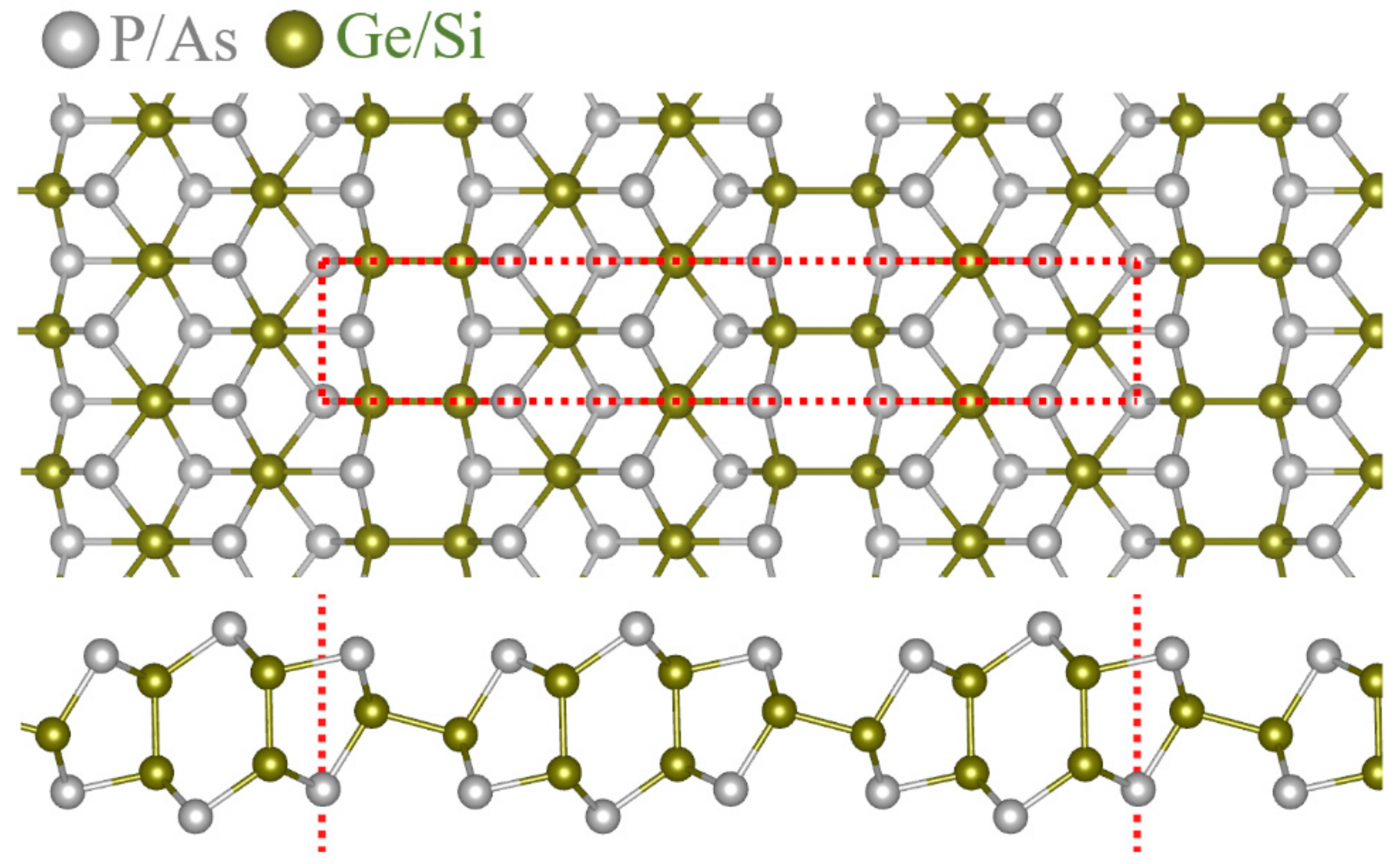
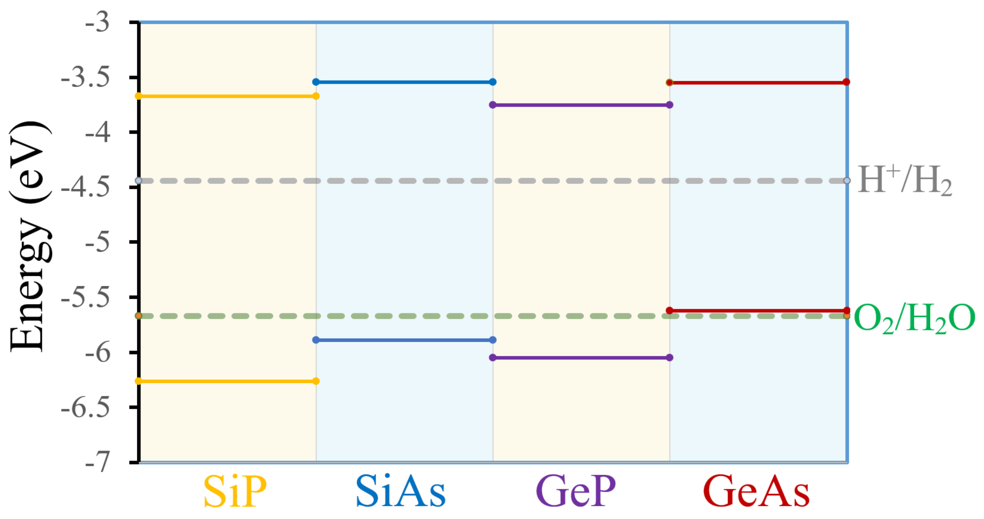
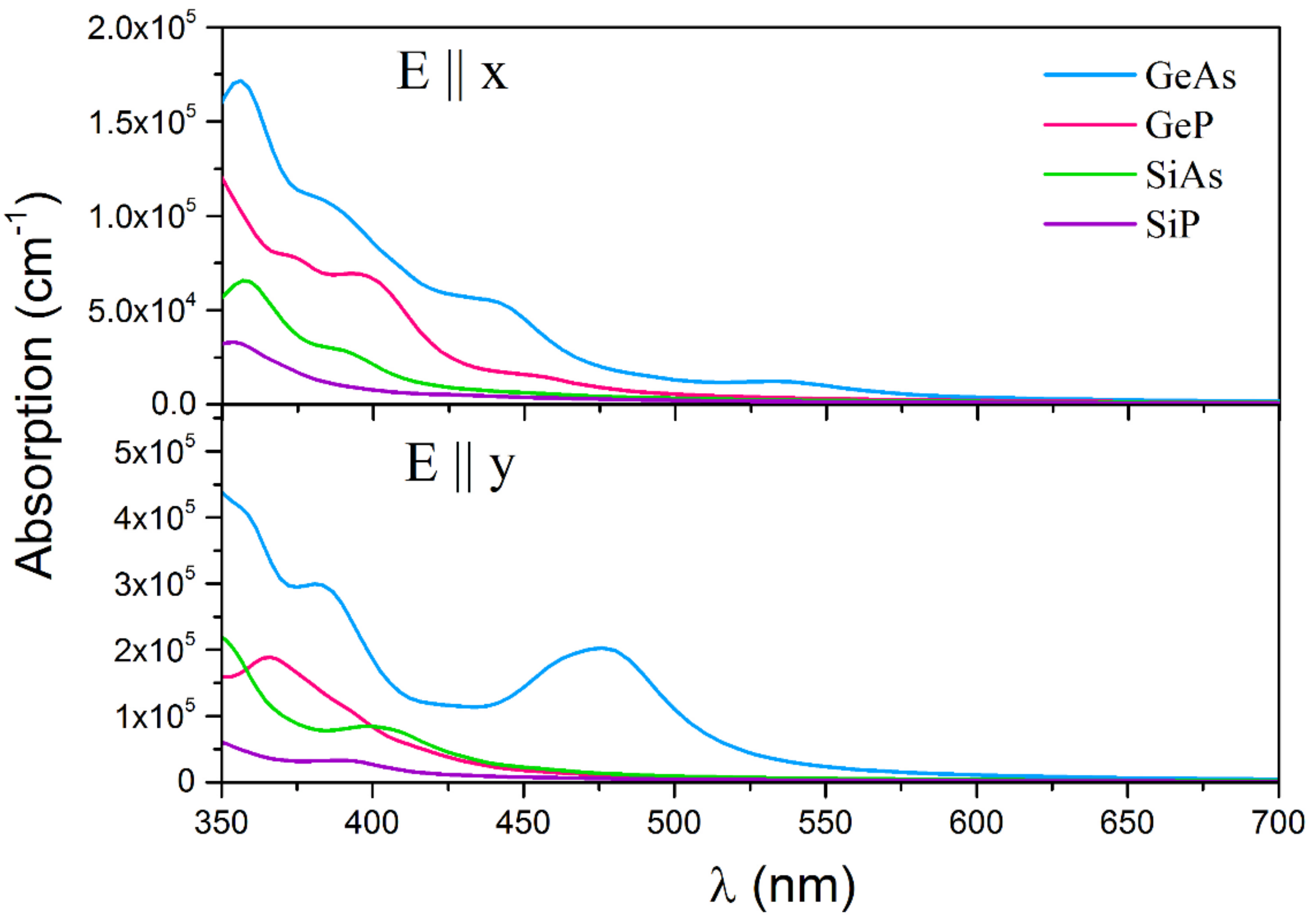
3. Results and Discussions

The top and side views of a sample of group IV–V-type 2D atomic lattices studied in this work are illustrated in Figure 1, which shows an ABC atomic stacking sequence. As discussed earlier, these structures show anisotropic atomic lattices and are highly elongated along one direction as compared with the perpendicular direction. The lattice constants along the elongated direction for SiP, SiAs, GeP and GeAs, were measured to be 20.54, 21.32, 21.49 and 22.25 Å, respectively. These values are around six-fold larger than the lattice constant along the perpendicular direction, calculated to be 3.53, 3.70, 3.66 and 3.82 Å, respectively.
We next probe the electronic properties of single-layer SiP, SiAs, GeP and GeAs by calculating the electronic band structures along the high symmetry directions according to the PBE/GGA approach, and the acquired results are depicted in Figure 2. Obtained results for the all studied nanosheets confirm that the valence band maximums (VBM) occur at the Γ-point in the Brillouin zone. For the SiP, SiAs and GeAs monolayers, the conduction band minimums (CBM) also coincide at the Γ-point, and thus these nanosheets can be categorized as direct band-gap semiconductors. As is clear, an exception exists for the case of GeP monolayer, in which the CBM occurs between the Γ-X path, resulting in an indirect band-gap. According to the PBE method, the electronic band-gaps of stress-free SiP, SiAs, GeP and GeAs monolayers were found to be 1.89, 1.69, 1.59 and 1.39 eV, respectively, which are in close agreement with the earlier study by Cheng et al. [21]. As it is eminent that the PBE/GGA underestimates the CBM edges, we also used HSE06 functional to more accurately estimate the electronic band structure and band-gap values. Interestingly, HSE06 method confirms the PBE/GGA estimations for the VBM and CBM positions, though the conductance bands are distinctly shifted up. On this basis, according to both PBE/GGA and HSE06 functional, SiP, SiAs and GeAs monolayers are direct band-gap semiconductors at the Γ-point, whereas GeP is an indirect band-gap material. The electronic band-gaps of stress-free and single-layer SiP, SiAs, GeP and GeAs were estimated to be 2.59, 2.34, 2.30 and 2.07 eV, respectively, using the HSE06 method.
We next shift our attention to assessing the suitability of these novel 2D systems for the solar water splitting. This process involves two redox half reactions:
Reduction: 2H+(aq.) + 2e → H2(g)
Oxidation: 2H2O → O2(g) + 4H+(aq.) + 4e
At pH equal to zero, the H+/H2 reduction potential and the O2/H2O oxidation potential are −4.44 and −5.67 eV, respectively, and thus the minimal required band-gap for the employment of a material in the solar water splitting process is 1.23 eV [48,49]. As is clear, with respect to the band-gap values, SiP, SiAs, GeP and GeAs nanosheets completely satisfy the prerequisite conditions. Nonetheless, as mentioned earlier, the configuration of band edges should be also taken into account when evaluating the applicability of a semiconductor for photocatalysis. On this basis, for a semiconducting material to be suitable for solar water splitting, it should pose a VBM less negative than the H+/H2 reduction potential and a CBM edge more negative than the O2/H2O oxidation potential. To explore the satisfaction of this important aforementioned factor, the CBM and VBM positions for the SiP, SiAs, GeP and GeAs monolayers along with the reduction H+/H2 and oxidation O2/H2O energy levels for the water splitting are illustrated in Figure 3. As is observable, SiP, SiAs and GeP nanosheets completely satisfy the required band positions, and a very slight overlap exists for the GeAs monolayer for the oxidation O2/H2O energy level. As is well-known, by increasing the pH from the zero (acidic condition), the H+/H2 and O2/H2O energy levels shift gradually to less negative values. This way, the GeAs nanosheets can also turn into a suitable candidate for the solar water splitting for the higher pHs than 0. It is worth reminding that the VBM edges for the SiP, SiAs and GeP are distinctly lower negative than the H+/H2 reduction potential energy for the zero pH. This way, by the increasing the pH, the suitability of the aforementioned nanosheets for the water splitting remains intact, which is an important observation.
Due to the asymmetric structures of studied monolayers, the optical spectra may show anisotropic behavior for the light polarizations along the x-axis (E||x) and y-axis (E||y). The absorption coefficients for the all studied monolayers for the light polarizations along the x- and y-axes are presented in Figure 4. It is conspicuous that along the y-axis, the adsorption is several times higher than the x-axis, confirming highly anisotropic optical properties in the studied nanosheets. From the results shown in Figure 4, it can be concluded that the absorption coefficient of the GeAs monolayer at visible range of light for both in-plane polarizations (E||x and E||y) is larger than those of other studied lattices. On the other hand, despite the indirect band-gap of GeP monolayer, its absorption coefficient is higher than SiAs and SiP monolayers. It is clear that XAs compounds show higher absorption coefficients than their XP counterparts. In general, the high absorption coefficients were attained on the order of 105 cm−1 for all structures along in-plane directions—this is an order of magnitude higher than a typical value for direct band gap semiconductors [50] across the entire UV−vis range. It is worth noting that the water-splitting absorbers must have the optimal band gap between 2.10 and 2.75 eV, with an optimum point at 2.26 eV. It is also worth noting that the values larger than 1.23 eV are essential to achieve solar-to-hydrogen efficiencies between 4% and 11% because of the losses related to the kinetic and entropic [51]. Our first-principles calculations indicate that the GeAs, GeP, SiAs and SiP nanosheets possess high absorption coefficient (α > 104 cm−1) in the visible range of light, which is higher than that of the typical absorption coefficient value for direct band-gap semiconductors and thus suggests them as highly promising candidates for the solar water splitting.
It is worth noting that the desirable electronic and optical characteristics of SiP, SiAs, GeP and GeAs nanosheets do not completely guarantee their practical successes for the application in water splitting devices. As has been discussed in recent studies [52,53], for the application in the water splitting, the employed materials should also exhibit stability under the water. Therefore, in the future theoretical and experimental studies, the stability of studied nanosheets under the water should be elaborately studied. For theoretical studies, relatively large composite molecular models have to be developed to address this aspect, which are extensively computationally demanding to be studied by the DFT-based simulations. To address the stability under the water, we do believe that classical molecular dynamics simulations by using the machine learning potentials [54,55,56] may show a great prospect.

4. Conclusions

Solar water splitting and the production of hydrogen fuel is currently considered as one of the most attractive green technologies to tackle the greenhouse environmental issues due to extensive consumption of fossil fuels. Low-symmetry 2D materials have recently garnered growing attention stemming from their unique direction-dependent transport properties. In this work we explored the application of SiP, SiAs, GeP and GeAs anisotropic nanosheets for the solar water splitting. The electronic band-gaps of stress-free and single-layer SiP, SiAs, GeP and GeAs were estimated to be 2.59, 2.34, 2.30 and 2.07 eV, respectively, which are within the desirable ranges for the water splitting. The studied nanosheets also satisfy the required band positions for the both H+/H2 and O2/H2O reactions, for a wide-range of environmental pHs. SiP, SiAs, GeP and GeAs nanomembranes were also predicted to adsorb visible range of light, with stupendously high absorption coefficients. The results provided by the first-principles density functional theory simulations highlight the outstanding prospects of SiP, SiAs, GeP and GeAs nanosheets for the design of next-generation hydrogen fuel nanogenerators.

Author Contributions

Conceptualization, B.M.; methodology, B.M.; Optical properties, M.S.; writing B.M.; supervision, G.C. and X.Z.; project administration, G.C. and X.Z.; funding acquisition, X.Z.

Funding

This research was funded by Deutsche Forschungsgemeinschaft (DFG, German Research Foundation) under Germany’s Excellence Strategy within the Cluster of Excellence PhoenixD (EXC 2122, Project ID 390833453).

Conflicts of Interest

The authors declare no conflict of interest.

References

  1. Novoselov, K.; Geim, A.K.; Morozov, S.; Jiang, D.; Zhang, Y.; Dubonos, S.V.; Grigorieva, I.V.; Firsov, A.A. Electric field effect in atomically thin carbon films. Science 2004, 306, 666–669. [Google Scholar] [CrossRef] [PubMed]
  2. Geim, A.K.; Novoselov, K.S. The rise of graphene. Nat. Mater. 2007, 6, 183–191. [Google Scholar] [CrossRef] [PubMed]
  3. Kubota, Y.; Watanabe, K.; Tsuda, O.; Taniguchi, T. Deep ultraviolet light-emitting hexagonal boron nitride synthesized at atmospheric pressure. Science 2007, 317, 932–934. [Google Scholar] [CrossRef] [PubMed]
  4. Song, L.; Ci, L.; Lu, H.; Sorokin, P.B.; Jin, C.; Ni, J.; Kvashnin, A.G.; Kvashnin, D.G.; Lou, J.; Yakobson, B.I.; et al. Large scale growth and characterization of atomic hexagonal boron nitride layers. Nano Lett. 2010, 10, 3209–3215. [Google Scholar] [CrossRef] [PubMed]
  5. Wang, Y.; Ding, Y. Strain-induced self-doping in silicene and germanene from first-principles. Solid State Commun. 2013, 155, 6–11. [Google Scholar] [CrossRef]
  6. Radisavljevic, B.; Radenovic, A.; Brivio, J.; Giacometti, V.; Kis, A. Single-layer MoS2 transistors. Nat. Nanotechnol. 2011, 6, 147–150. [Google Scholar] [CrossRef]
  7. Watts, M.C.; Picco, L.; Russell-Pavier, F.S.; Cullen, P.L.; Miller, T.S.; Bartuś, S.P.; Payton, O.D.; Skipper, N.T.; Tileli, V.; Howard, C.A. Production of phosphorene nanoribbons. Nature 2019, 568, 216–220. [Google Scholar] [CrossRef]
  8. Gusmão, R.; Sofer, Z.; Pumera, M. Functional protection of exfoliated black phosphorus by noncovalent modification with anthraquinone. ACS Nano 2018, 12, 5666–5673. [Google Scholar] [CrossRef]
  9. Sturala, J.; Sofer, Z.; Pumera, M. Chemistry of layered pnictogens: Phosphorus, arsenic, antimony, and bismuth. Angew. Chem. Int. Ed. 2019, 131, 7551–7557. [Google Scholar] [CrossRef]
  10. Ares, P.; Palacios, J.J.; Abellán, G.; Gómez-Herrero, J.; Zamora, F. Recent progress on antimonene: A new bidimensional material. Adv. Mater. 2018, 30, 1703771. [Google Scholar] [CrossRef]
  11. Jariwala, D.; Sangwan, V.K.; Lauhon, L.; Marks, T.J.; Hersam, M.C. Emerging device applications for semiconducting two-dimensional transition metal dichalcogenides. ACS Nano 2014, 8, 1102–1120. [Google Scholar] [CrossRef] [PubMed]
  12. Mohammad, R.; Kenneth, D.; Shi-Zhang, Q. Advent of 2D rhenium disulfide (ReS2): Fundamentals to applications. Adv. Funct. Mater. 2017, 27, 1606129. [Google Scholar] [CrossRef]
  13. Shengxue, Y.; Yanhan, Y.; Minghui, W.; Chunguang, H.; Wanfu, S.; Yongji, G.; Li, H.; Chengbao, J.; Yongzhe, Z. Highly in-plane optical and electrical anisotropy of 2D germanium arsenide. Adv. Funct. Mater. 2018, 28, 1707379. [Google Scholar] [CrossRef]
  14. Liu, E.; Fu, Y.; Wang, Y.; Feng, Y.; Liu, H.; Wan, X.; Zhou, W.; Wang, B.; Shao, L.; Ho, C.H.; et al. Integrated digital inverters based on two-dimensional anisotropic ReS2 field-effect transistors. Nat. Commun. 2015, 6, 6991. [Google Scholar] [CrossRef] [PubMed]
  15. Yan, J.; Hu, M.; Li, D.; He, Y.; Zhao, R.; Jiang, X.; Song, S.; Wang, L.; Fan, C. A nano and micro-integrated protein chip based on quantum dot probes and a microfluidic network. Nano Res. 2008, 1, 490–496. [Google Scholar] [CrossRef]
  16. Yang, H.; Jussila, H.; Autere, A.; Komsa, H.P.; Ye, G.; Chen, X.; Hasan, T.; Sun, Z. Optical waveplates based on birefringence of anisotropic two-dimensional layered materials. ACS Photonics 2017, 4, 3023–3030. [Google Scholar] [CrossRef]
  17. Beck, C.G. Crystallography of SiP and SiAs single crystals and of SiP precipitates in Si. J. Appl. Phys. 1966, 37, 4683. [Google Scholar] [CrossRef]
  18. Donohue, P.C.; Young, H.S. Synthesis, structure, and superconductivity of new high pressure phases in the systems GeP and GeAs. J. Solid State Chem. 1970, 1, 143–149. [Google Scholar] [CrossRef]
  19. Ashton, M.; Sinnott, S.B.; Hennig, R.G. Computational discovery and characterization of polymorphic two-dimensional IV–V materials. Appl. Phys. Lett. 2016, 109, 192103. [Google Scholar] [CrossRef]
  20. Liang, L.; Weike, W.; Penglai, G.; Xiangde, Z.; Bei, D.; Xingqiang, S.; Guoying, G.; Huiqiao, L.; Tianyou, Z. 2D GeP: An unexploited low-symmetry semiconductor with strong in-plane anisotropy. Adv. Mater. 2018, 30, 1706771. [Google Scholar] [CrossRef]
  21. Cheng, A.Q.; He, Z.; Zhao, J.; Zeng, H.; Chen, R.S. Monolayered silicon and germanium monopnictide semiconductors: Excellent stability, high absorbance, and strain engineering of electronic properties. ACS Appl. Mater. Interfaces 2018, 10, 5133–5139. [Google Scholar] [CrossRef] [PubMed]
  22. Mortazavi, B.; Rabczuk, T. Anisotropic mechanical properties and strain tuneable band-gap in single-layer SiP, SiAs, GeP and GeAs. Phys. E Low Dimens. Syst. Nanostruct. 2018, 103, 273–278. [Google Scholar] [CrossRef] [Green Version]
  23. Chen, Q.Y.; Cao, C.; He, Y. Optical anisotropy and strain tunable optical, electronic and structural properties in monolayer GeP: A computational study. Phys. E Low Dimens. Syst. Nanostruct. 2019, 113, 172–180. [Google Scholar] [CrossRef]
  24. Wang, X.; Deng, G.; Yu, W.; Wang, B.; Li, X.; Liu, Y.; Zhao, Y.; Wang, Q.; Zhang, L.; Cai, X. A class of two-dimensional SiAs monolayers with novel electronic and optical properties from ab initio investigations. Eur. Phys. J. Plus 2019, 134, 287. [Google Scholar] [CrossRef]
  25. Shi, L.B.; Cao, S.; Yang, M. Strain behavior and carrier mobility for novel two-dimensional semiconductor of GeP: First principles calculations. Phys. E Low Dimens. Syst. Nanostruct. 2019, 107, 124–130. [Google Scholar] [CrossRef]
  26. Shojaei, F.; Hahn, J.R.; Kang, H.S. Electronic structure and photocatalytic band offset of few-layer GeP2. J. Mater. Chem. A 2017, 5, 22146–22155. [Google Scholar] [CrossRef]
  27. Mortazavi, H. Could art therapy reduce the death anxiety of patients with advanced cancer? An interesting question that deserves to be investigated. Indian J. Palliat. Care 2018, 24, 387–388. [Google Scholar] [CrossRef]
  28. Shojaei, F.; Kang, H.S. Electronic structures and Li-diffusion properties of group IV-V layered materials: Hexagonal germanium phosphide and germanium arsenide. J. Phys. Chem. C 2016, 120, 23842–23850. [Google Scholar] [CrossRef]
  29. Tabatabaeichehr, M.; Mortazavi, H.; Abadi, M.H.; Moayed, L. Sexual desire and related factors in middle-aged and elderly married women: A cross-sectional study in Iran. Open Access Maced. J. Med Sci. 2018, 6, 1906–1911. [Google Scholar] [CrossRef]
  30. Tagani, M.B. Electrical and mechanical properties of a fully hydrogenated two-dimensional polyaniline sheet. Comput. Mater. Sci. 2018, 153, 126–133. [Google Scholar] [CrossRef]
  31. Tagani, M.B.; Vishkayi, S.I. Polyaniline (C3N) nanoribbons: Magnetic metal, semiconductor, and half-metal. J. Appl. Phys. 2018, 124, 84304. [Google Scholar] [CrossRef] [Green Version]
  32. Vishkayi, S.I.; Tagani, M.B. Current-voltage characteristics of borophene and borophane sheets. Phys. Chem. Chem. Phys. 2017, 19, 21461–21466. [Google Scholar] [CrossRef]
  33. Bafekry, A.; Shayesteh, S.F.; Peeters, F.M. C3N monolayer: Exploring the emerging of novel electronic and magnetic properties with adatom adsorption, functionalizations, electric field, charging, and strain. J. Phys. Chem. C 2019, 123, 12485–12499. [Google Scholar] [CrossRef]
  34. Peng, Y.; Li, J.; Tang, X.; Yang, W.; Chen, X.; Fan, C.; Wang, K. Molecular dynamics study on the tribological properties of phosphorene/polyethylene composites. Coatings 2019, 9, 342. [Google Scholar] [CrossRef]
  35. Liu, T.; Qin, H.; Yang, D.; Zhang, G. First principles study of gas molecules adsorption on monolayered β-SnSe. Coatings 2019, 9, 390. [Google Scholar] [CrossRef]
  36. Bafekry, A.; Ghergherehchi, M.; Shayesteh, S.F.; Peeters, F. Adsorption of molecules on C3N nanosheet: A first-principle calculations. Chem. Phys. 2019, 526, 110442. [Google Scholar] [CrossRef]
  37. Shi, L.B.; Yang, M.; Cao, S.; You, Q.; Niu, Y.Y.; Wang, Y.Z. Elastic behavior and intrinsic carrier mobility for monolayer SnS and SnSe: First-principles calculations. Appl. Surf. Sci. 2019, 492, 435–448. [Google Scholar] [CrossRef]
  38. Makaremi, M.; Grixti, S.; Butler, K.T.; Ozin, G.A.; Singh, C.V. Band engineering of carbon nitride monolayers by N-Type, P-Type, and isoelectronic doping for photocatalytic applications. ACS Appl. Mater. Interfaces 2018, 10, 11143–11151. [Google Scholar] [CrossRef]
  39. Bafekry, A.; Ghergherehchi, M.; Shayesteh, S.F. Tuning the electronic and magnetic properties of antimonene nanosheets via point defects and external fields: First-principles calculations. Phys. Chem. Chem. Phys. 2019, 21, 10552–10566. [Google Scholar] [CrossRef]
  40. Kresse, G.; Joubert, D. From ultrasoft pseudopotentials to the projector augmented-wave method. Phys. Rev. B 1999, 59, 1758–1775. [Google Scholar] [CrossRef]
  41. Kresse, G.; Furthmüller, J. Efficiency of ab-initio total energy calculations for metals and semiconductors using a plane-wave basis set. Comput. Mater. Sci. 1996, 6, 15–50. [Google Scholar] [CrossRef]
  42. Kresse, G.; Furthmüller, J. Efficient iterative schemes for ab initio total-energy calculations using a plane-wave basis set. Phys. Rev. B 1996, 54, 11169–11186. [Google Scholar] [CrossRef] [PubMed]
  43. Perdew, J.; Burke, K.; Ernzerhof, M. Generalized gradient approximation made simple. Phys. Rev. Lett. 1996, 77, 3865–3868. [Google Scholar] [CrossRef] [PubMed]
  44. Blöchl, P.E.; Jepsen, O.; Andersen, O.K. Improved tetrahedron method for Brillouin-zone integrations. Phys. Rev. B 1994, 49, 16223–16233. [Google Scholar] [CrossRef] [PubMed]
  45. Monkhorst, H.J.; Pack, J.D. Special points for Brillouin-zone integrations. Phys. Rev. B 1976, 13, 5188–5192. [Google Scholar] [CrossRef]
  46. Krukau, A.V.; Vydrov, O.A.; Izmaylov, A.F.; Scuseria, G.E. Influence of the exchange screening parameter on the performance of screened hybrid functionals. J. Chem. Phys. 2006, 125, 224106. [Google Scholar] [CrossRef] [PubMed]
  47. Shahrokhi, M. Quasi-particle energies and optical excitations of ZnS monolayer honeycomb structure. Appl. Surf. Sci. 2016, 390, 377–384. [Google Scholar] [CrossRef]
  48. Tachibana, Y.; Vayssieres, L.; Durrant, J.R. Artificial photosynthesis for solar water-splitting. Nat. Photonics 2012, 6, 511–518. [Google Scholar] [CrossRef]
  49. Lewis, N.S.; Nocera, D.G. Powering the planet: Chemical challenges in solar energy utilization. Proc. Natl. Acad. Sci. USA 2006, 103, 15729–15735. [Google Scholar] [CrossRef] [PubMed] [Green Version]
  50. Kreher, K. Fundamentals of semiconductors—physics and materials properties. Z. Phys. Chem. 1997, 198, 275. [Google Scholar] [CrossRef]
  51. Seitz, L.C.; Chen, Z.; Forman, A.J.; Pinaud, B.A.; Benck, J.D.; Jaramillo, T.F. Modeling practical performance limits of photoelectrochemical water splitting based on the current state of materials research. ChemSusChem 2014, 7, 1372–1385. [Google Scholar] [CrossRef] [PubMed]
  52. Singh, A.K.; Zhou, L.; Shinde, A.; Suram, S.K.; Montoya, J.H.; Winston, D.; Gregoire, J.M.; Persson, K.A. Electrochemical stability of metastable materials. Chem. Mater. 2017, 29, 10159–10167. [Google Scholar] [CrossRef]
  53. Jain, A.; Wang, Z.; Nørskov, J.K. Stable two-dimensional materials for oxygen reduction and oxygen evolution reactions. ACS Energy Lett. 2019, 4, 1410–1411. [Google Scholar] [CrossRef]
  54. Gubaev, K.; Podryabinkin, E.V.; Hart, G.L.; Shapeev, A.V. Accelerating high-throughput searches for new alloys with active learning of interatomic potentials. Comput. Mater. Sci. 2019, 156, 148–156. [Google Scholar] [CrossRef]
  55. Kostiuchenko, T.; Körmann, F.; Neugebauer, J.; Shapeev, A. Impact of lattice relaxations on phase transitions in a high-entropy alloy studied by machine-learning potentials. Npj Comput. Mater. 2019, 5, 55. [Google Scholar] [CrossRef] [Green Version]
  56. Podryabinkin, E.V.; Tikhonov, E.V.; Shapeev, A.V.; Oganov, A.R. Accelerating crystal structure prediction by machine-learning interatomic potentials with active learning. Phys. Rev. B 2019, 99, 064114. [Google Scholar] [CrossRef] [Green Version]
Figure 1. A sample of SiP, SiAs, GeP and GeAs atomic lattice. The unit-cell is shown with a dashed red line.
Coatings 09 00522 g001
Figure 2. Electronic band structures of single-layer and free-standing (a) SiP, (b) SiAs, (c) GeP and (d) GeAs predicted by the Perdew–Burke–Ernzerhof (PBE)/generalized gradient approximation (GGA) (continuous lines) and HSE06 (black dotted lines) functional. The Fermi energy is aligned to zero.
Coatings 09 00522 g002
Figure 3. Conduction band minimums (CBM) and valence band maximums (VBM) positions (continuous lines) for the SiP, SiAs, GeP and GeAs monolayers along with the reduction H+/H2 and oxidation O2/H2O energy levels (shown with dashed limits) for the water splitting at pH equal to zero.
Coatings 09 00522 g003
Figure 4. Absorption coefficient of GeAs, GeP, SiAs and SiP monolayers as a function of the wavelength (λ) along the x and y polarization directions according to RPA + HSE06 estimations.
Coatings 09 00522 g004

