1. Introduction
The low-temperature photoluminescence (PL) of CdTe single crystals has been intensively studied in the past [
1,
2]. It is very well known that the typical low-temperature spectrum of undoped single-crystal CdTe consists of bands assigned to the recombination of free excitons (FX), bound excitons (AX or DX), free-to-bound transitions (FB), and donor–acceptor pair (DAP) transitions. Fewer low-temperature PL studies have been conducted for polycrystalline CdTe, which has been established as a very promising photovoltaic material for thin film solar cells [
3,
4]. A typical CdTe solar cell consisting of a CdS/CdTe layer grown on a SnO
2/glass substrate is based on recombination within an n-CdS/p-CdTe heterojunction. Despite a 9.7% lattice mismatch occurring between the hexagonal CdS and the cubic CdTe, high-efficiency devices result from this junction, probably due to interdiffusion at the CdS/CdTe interface [
5,
6,
7,
8]. The S may passivate the grain boundaries and relieve the lattice mismatch between CdS and CdTe, thereby reducing recombination and improving device performance.
It is very well known that the post-deposition CdCl
2 annealing step is required to make reasonably efficient CdTe solar cells. It has been suggested that the CdCl
2 treatment enlarges grains, causes recrystallization, and enhances the diffusion of S from CdS into CdTe at the interface [
2,
7]. Additionally, the presence of chlorine dopants creates new recombination centers that may affect the recombination processes of photogenerated electron–hole pairs. It has been reported that the CdCl
2 treatment introduces two very important chlorine related defects, such as chlorine substituting on a tellurium site (Cl
Te) donor center and a V
Cd-Cl
Te (A) acceptor center that can be identified in the PL spectrum [
1,
5,
9,
10].
It was found recently that further improvement of CdTe solar cell can be achieved by Cu doping [
11,
12,
13,
14,
15,
16]. Cu enters the CdTe interstitially forming a shallow donor, Cu
i centers and gives rise to deep acceptor Cu
Cd centers via substitution [
12,
13,
14,
15].
In this paper, results of studies on the effect of Cu doping on the low-temperature front side PL of CdS/CdTe solar cells will be presented.
2. Experimental Design
2.1. Film Deposition and Cell Fabrication
Cadmium telluride solar cells were fabricated in the superstrate configuration with the structure: glass/TCO/n
+-CdS/p-CdTe/graphite/metal back contact in our laboratory (CNBM Center). Commercially available soda-lime glass coated with SnO
2:F/HRT was used as a substrate for the depositions. CdS (~80 nm in thickness) was deposited by chemical bath deposition (CBD) at 88 °C using cadmium chloride, thiourea, ammonium acetate, and ammonia, followed by annealing at 400 °C. CdTe (6–10 μm in thickness) was deposited by close-spaced sublimation (CSS) at
Ts = 600 °C using graphite susceptors in 10–15 Torr He/O
2. The CdTe was then soaked in CdCl
2/methanol at 80 °C, followed by a furnace anneal under controlled conditions (380 °C, He/O
2, 300 Torr) in order to improve the CdTe structure and minority carrier lifetime. To form the back contact, a nitric-phosphoric (NP) acid etch was used to remove the surface oxide, and a very thin layer of Cu was evaporated. The efficiency of the cells examined in this work was in the range of 10%–11%. The overall process is described in [
17].
A schematic of a typical CdS/CdTe solar cell is shown in
Figure 1.
2.2. Photoluminescence Measurements
The PL spectra were measured for undoped and Cu-doped CdTe/CdS cells produced from the CdTe source with a purity of 99.999% (5N) or 99.99999% (7N) and illuminated by monochromatic light directed onto the backside or front side of the solar cell structure. All measurements were performed on CdCl2-treated cell structures, but before the deposition of the back contact.
For the backside PL, the measurements were taken by illuminating the CdTe/CdS cells with a 658 nm line generated by a red laser diode (LPM658, Newport, Irvine, CA, USA). For the front side luminescence, in addition to red excitation, a blue line with a wavelength of 405 nm (laser diode LQA405-8SE, Newport, Irvine, CA, USA) was also used. In Cu-doped samples, Cu was introduced to the cell through diffusion at 400 °C from a layer of pure metal deposited on the CdTe after chlorine treatment. The thickness of the copper layer was 10 nm. All of the samples used for PL measurements were placed in a closed-cycle cryostat with a controlled temperature ranging from 10 to 300 K. Spectra were recorded using a grated monochromator coupled to a cooled photomultiplier tube (R106999, Hamamatsu, Tokyo, Japan).
3. Experimental Results and Discussion
3.1. Optical Characterization of the CdS/CdTe Solar Cells
In
Figure 2, the results of the backside PL excited by 658 nm light are shown for two different CdS/CdTe samples. One sample was a solar cell grown in the NREL laboratory (Golden, Colorado, USA) and kindly supplied to us for testing. The second sample was grown in the CNBM Center using the same methodology used to generate solar cell devices with an efficiency of about 11%. As can be seen in
Figure 2, the spectra obtained from both samples were similar. The presence of an excitonic band with a maximum at 1.59 eV indicated good-quality CdTe polycrystalline films in both samples. In both samples, defect-related peaks observed at around 1.44 eV were recorded. The defect-related peaks were assigned to DAP transitions between the Cl
Te donor centers and the A acceptor centers [
1,
10]. The origin of the peaks between 1.55 and 1.50 eV in both samples is still under discussion. A similar emission behavior was reported by other authors [
1,
10] who assigned bands in this region to DAP transitions (1.56 eV) and free electron–acceptor (e, A
0) transitions (1.54 eV).
3.2. Front Side Luminescence of CdS/CdTe Structure Excited by a 658 nm (1.88 eV) Line
For front side luminescence, solar cells were illuminated from the front side of the device consisting of glass covered by TCO and a CdS window transparent to excitation light of 658 nm. However, the excitation light was strongly absorbed by the CdTe layer. Due to the high absorption, the generation of free electron–hole pairs and their subsequent separation or recombination occurred exclusively in a very narrow layer of the CdTe adjacent to the CdS/CdTe interface. Front side PL, called junction luminescence, gives us direct information about processes occurring in this area.
3.2.1. Front Side Luminescence of an Undoped CdS/CdTe
Figure 3 shows the PL spectrum obtained for the undoped CdS/CdTe structure excited from the junction side through the glass. The backside PL spectrum obtained for the same sample is shown for comparison. The junction PL of undoped CdS/CdTe structures has been reported by several investigators [
10,
11,
18,
19] and results similar to ours were obtained. The front side spectrum consists of two peaks at 1.53 and 1.43 eV; the high-energy peak at 1.59 eV detected in the backside spectrum is not present. There are two possible explanations for this observation. One possibility is to assume that the origin of the 1.53 eV peak in the junction PL and the 1.59 eV peak in the backside PL is the same, namely that they are both due to bound-exciton emission. The 73 MeV shift in the exciton peak towards a lower energy for the junction region can be attributed to the reduction of the bandgap due to the formation of the CdS
xTe
1−x alloy at the interface described in [
7,
8,
9,
10]. The shift found in this paper is similar to that found in [
19,
20].
The alternative explanation is to assume that the excitonic band at 1.59 eV is depressed due to a high density in defects at the interface and that the 1.53 eV peak is equivalent to the broad free-to-bound peak around 1.56 eV detected in the same sample excited from the back. However, the analysis of the temperature dependence of the intensity of the 1.53 eV peak presented in the next section strongly favors the assertion of an excitonic origin of this peak.
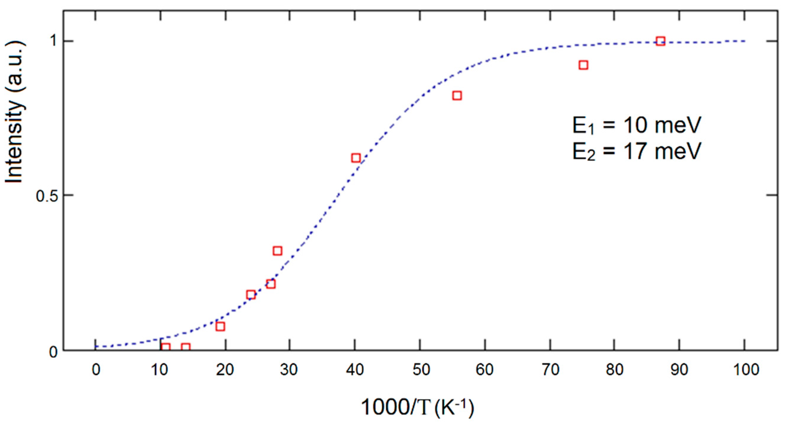
3.2.2. Temperature Dependence of the 1.53 eV Peak
In order to further clarify the origin of the 1.53 eV peak found in the junction PL of the undoped sample, additional measurements of PL as a function of temperature were conducted. The analysis of the temperature dependence of the intensity of the 1.53 eV transition presented in
Figure 4 shows a good fit with a two activation-energy model:
proposed by Bimberg et al. [
20] for the temperature decay of bound excitons. The activation energies
E1 and
E2 in this equation represent the electron–hole binding energy and the binding energy of the exciton to the impurity, respectively.
The binding energy of 10 meV is in good agreement with the binding energy of the free exciton [
1], and it is reasonable to assume that the 17 meV point represents the binding energy of the exciton to the unidentified acceptor or the chlorine donor. The exciton position of 1.53 eV and the two binding energies, 0.01 and 0.017 eV, can be used to calculate the energy gap for CdS
xTe
1−x alloy [
1]:
Following the work of Ohata [
21] and Pal [
22], the composition of such alloy can be predicted using a simple quadratic equation:
Assuming
k = 1.7 eV from [
21] and substituting a 10 K bandgap for CdS (
Eg (CdS) = 2.59 e) and for that of CdTe (
Eg (CdTe) = 1.61 eV), the value
x ≅ 0.08 can be obtained.
3.2.3. Effect of Cu on the Front Side Luminescence of CdS/CdTe Solar Cells
The effect of Cu on the solar cell structure was studied by measuring the front side PL from a sample with a 10 nm Cu layer deposited on the CdTe side of the cell that was subjected to chlorine treatment, as described previously. After Cu deposition, the cell was annealed for 10 min at 400 °C. As can be seen from the
Figure 5, in addition to peaks at 1.43 and 1.53 eV observed in the undoped samples, two new peaks at 1.595 and 1.56 eV were recorded in the Cu-doped samples. The following conclusions can be drawn from the comparison of the spectra taken for doped and undoped samples:
It is worth noting that a similar effect has not been found in previously reported studies [
11,
18,
19] of front side luminescence of Cu-doped CdTe/CdS solar cells. This may suggest that the Cu did not reach the junction area in those samples.
3.3. Front Side Luminescence of CdS/CdTe Structure Excited by a 405 nm (3.06 eV) Line
3.3.1. Front Side Luminescence of an Undoped CdS/CdTe Structure
Contrary to red light, blue light is strongly absorbed by the CdS layer. Therefore, it is reasonable to assume that the PL shown in
Figure 6 is related mainly to emission from the CdS layer. In a high energy range, four peaks with maximal emission at 2.34, 1.92, 1.79 eV and a weak emission at 1.65 eV were recorded. Despite the extensive literature on the luminescence of polycrystalline thin film CdS, the interpretation of the observed PL bands may not be easy. The low-temperature PL strongly depends on the type of deposition and the post-deposition treatment [
26,
27]. According to the literature data [
26], it is reasonable to assume that the emission at around 2.34 eV can be attributed to the excitons bound to substitutional Te atoms on the sulfur lattice site while the two bands at 1.79 and 1.65 eV may be due to a DAP transition involving Te complexes in the CdS. The peak at 1.92 eV had a similar position to what has been called a red band, ascribed to V
Cd-V
s defects [
26].
In the low energy range, two strong peaks at 1.51 and 1.41 eV were detected. The origin of those peaks is not clear. They may be related to an emission from CdTe as the position of those peaks are similar to that recorded for the front side PL excited by red light. On the other hand, similar peaks were found in polycrystalline CdS grown on glass or TCO by chemical bath deposition [
26], and were ascribed to the transition of electrons trapped in surface states to the valence band.
3.3.2. Effect of Cu on the Front Side Luminescence of CdS/CdTe Solar Cells
The effect of Cu doping on CdS luminescence has never been studied before. As can be seen from
Figure 6, the intensity of all four high energy peaks increased significantly due to Cu doping but no peak shift was observed. This can be understood assuming that the Cu passes through the interface and diffuses into the CdS film, where it reacts with native CdS defects in such way that the number of nonradiative recombination events decreases. The decrease in the intensity of the peaks at 1.51 and 1.41 eV in doped samples suggests that those peaks are related to the CdS lattice rather than to the CdTe. The reduction of the intensity of the peaks can be ascribed to the reduction in the number of surface defects in the Cu-doped sample.
4. Conclusions
Low-temperature junction PL has been used to study the effect of Cu deposited on CdTe on the electronic structure of CdTe/CdS solar cells grown in our laboratory.
In undoped cells, good evidence for the interdiffusion of sulfur and bandgap reduction was found in CdTe/CdS solar cells subjected to CdCl2 treatment. The energy gap of 1.557 eV was calculated and the composition of the interface alloy was estimated to be x ≅ 0.08.
In Cu-doped samples, the junction PL data provides evidence that Cu diffuses into the junction area, forming CuCd centers. The most interesting result of this work is the fact that the energy bandgap of CdTe at the interface restores its original value of about 1.60 eV. This allows us to suggest that the presence of Cu in the junction area hinders the interdiffusion of sulfur through the interface. If so, the effect of sulfur diffusion on the cell performance should be reexamined.
Finally, this is the first time that CU has been documented to diffuse through the interface into the CdS layer, changing the character of the recombination processes in the CdS.
Author Contributions
Conceptualization, H.O. and D.C.; Methodology, H.O.; Validation, H.O.; Formal Analysis, H.O. and D.C.; Investigation, D.C.; resources, Z.C.; Data Curation, H.O.; Writing—Original Draft Preparation, H.O.; Writing—Review and Editing, H.O., D.C. and Z.C.; Visualization, D.C. and H.O.; Supervision, K.C.; Project Administration, H.O. and K.C.; Funding Acquisition, K.C.
Funding
This research was funded by China Triumph International Engineering CO. LTD.
Acknowledgments
The authors thank the National Renewable Energy Laboratory, Golden, Colorado 80401 for supplying CdTe/CdS solar cells for reference measurements and members of the NJIT CNBM research center for processing help and useful discussions. In particular, the authors wish to thank Zhitao Wang for his involvement in taking PL measurements for this work.
Conflicts of Interest
The authors declare no conflict of interest.
References
- Liu, X. Photoluminecence and Extended X-ray Absoprtion Fine Structure Studies on CdTe Material. Ph.D. Thesis, University of Toledo, Toledo, OH, USA, 2006. [Google Scholar]
- Dhere, R.G. Study of the CdS/CdTe Interface and Its Relevance to Solar Cell Properties. Ph.D. Thesis, University of Colorado, Boulder, CO, USA, 1997. [Google Scholar]
- Wu, X. High-efficiency polycrystalline CdTe thin film solar cells. Sol. Energy 2004, 77, 803–814. [Google Scholar] [CrossRef]
- Bosio, A.; Rosa, G.; Romeo, N. Past, present, and future of the thin film CdTe/CdS solar cells. Sol. Energy 2018, 175, 31–43. [Google Scholar] [CrossRef]
- Potter, M.D.G.; Cousins, M.; Durose, K.; Halliday, D.P. Effect of interdiffusion and impurities on thin film CdTe/CdS photovoltaic junction. J. Mater. Sci. Mater. Electron. 2000, 11, 525–530. [Google Scholar] [CrossRef]
- Moutinho, H.R.; Dhere, R.G.; Jiang, C.S.; Albin, D.S.; Al-Jassim, M.M. Electrical properties of DcTe/CdS and CdTe/SnO2 solar cells studied with scanning kelvin probe microscopy. In Proceedings of the 35th Photovoltaic Specialists Conference, Honolulu, HI, USA, 20–25 June 2010; p. 1955. [Google Scholar]
- Metzger, W.K.; Albin, D.; Romero, M.J.; Dippo, P.; Young, M. CdCl2 treatment, S diffusion, and recombination in polycrystalline CdTe. J. Appl. Phys. 2006, 99, 103703–103708. [Google Scholar] [CrossRef]
- Delahoy, A.E.; Cheng, Z.; Chin, K. Evidence for CdTe1−xSx Compound formation in CdTe solar cells from high-precision, temperature-dependent device measurements. In Proceedings of the 39nd Photovoltaic Specialist Coonference, Tampa, FL, USA, 16–21 June 2013; pp. 1945–1948. [Google Scholar]
- Van Gheluwe, J.; Versluys, D.; Poelman, P.; Clauws, P. Photoluminescence study of polycrystalline CdS/CdTe thin solar cells. Thin Solid Film. 2005, 480, 264–268. [Google Scholar] [CrossRef]
- Okamoto, T.; Matsuzaki, Y.; Amin, N.; Yamada, A.; Konagai, M. Characterization of highly efficient CdTe thin film solar cells by low-temperature photoluminescence. Jpn. J. Appl. Phys. 1998, 7, 3894–3899. [Google Scholar] [CrossRef]
- Okamoto, T.; Yamada, A.; Konagai, M. Optical and electrical characterization of highly efficient CdTe thin film solar cells. Thin Solid Film. 2001, 387, 6–10. [Google Scholar] [CrossRef]
- Grecu, D.; Compan, A.D.; Young, D.; Jayamaha, U.; Rose, D.H. Photoluminescence of Cu-doped CdTe and related stability issues in CdS/CdTe solar cells. J. Appl. Phys. 2000, 88, 2490–2496. [Google Scholar] [CrossRef]
- Demtsu, S.H.; Albin, D.S.; Sites, J.R.; Metzger, W.K.; Duda, A. Cu-related recombination in CdS/CdTe solar cell. Thin Solid Film. 2008, 516, 2251–2254. [Google Scholar] [CrossRef]
- Okamoto, T.; Hayashi, R.; Hara, S.; Ogawa, Y. Cu doping of CdTe layers in polycrystalline CdTe thin-film solar cells for top cells of multijunction solar cells. Jpn. J. Appl. Phys. 2013, 52, 102301. [Google Scholar] [CrossRef]
- Perrenoud, J.; Kranz, L.; Gretener, C.; Pianezzi, F.; Nishiwaki, A.; Buecheler, S.; Tiwari, A.N. A comprehensive picture of cu doping in CdTe solar cells. J. Appl. Phys. 2013, 114, 174505–174525. [Google Scholar] [CrossRef]
- Kuciauskas, D.; Kanevce, A.; Duenow, J.N.; Dippo, P.; Young, M.; Li, J.V.; Levi, D.H.; Gessert, T.A. Spectrally and time resolved photoluminescence analysis of the CdS/CdTe interface in thin-film photovoltaic solar cells. Appl. Phys. Lett. 2013, 102, 173902. [Google Scholar] [CrossRef]
- Kharangarh, P.R.; Misra, D.; Georgiou, G.E.; Chin, K.K. Characterization of space charge layer deep defects in n+-CdS/p-CdTe solar cells by temperature dependent capacitance spectroscopy. J. Appl. Phys. 2013, 113, 144504–144509. [Google Scholar] [CrossRef]
- Kuciauskas, D.; Dippo, D.; Kanevce, A.; Zhao, Z.; Cheng, L.; Los, A.; Gloeckler, M.; Metzger, W.K. The impact of Cu on recombination in high voltage CdTe solar cells. Appl. Phys. Lett. 2015, 107, 243906. [Google Scholar] [CrossRef]
- Kuciauskas, D.; Dippo, D.; Zhao, Z.; Cheng, L.; Kanevce, A.; Metzger, W.K.; Gloeckler, M. Recombination analysis in cadmium telluride photovoltaic solar cells with photoluminecence spectroscopy. IEEE J. Photovolt. 2016, 6, 313–319. [Google Scholar] [CrossRef]
- Bimberg, D.; Sondergeld, M.; Grobe, E. Thermal dissociation of excitons bounds to neutral acceptors in high-purity GaAs. Phys. Rev. B 1971, 4, 3451–3455. [Google Scholar] [CrossRef]
- Ohata, K.; Saraie, J.; Tanaka, T. Optical energy gap of the mixed crystal CdSxTe1−x. Jpn. J. Appl. Phys. 1973, 12, 1641. [Google Scholar] [CrossRef]
- Pal, R.; Dutta, J.; Chaudhuri, S.; Pal, A. CdSxTe1−x films: Preparation and properties. J. Phys. D Appl. Phys. 1993, 26, 704–710. [Google Scholar] [CrossRef]
- Molva, E.; Chamonal, J.P.; Saminadayar, K.; Pajot, B.; Neu, G. Excited states of Ag an Cu acceptors in CdTe. Solid State Commun. 1982, 44, 351–355. [Google Scholar] [CrossRef]
- Laurenti, J.P.; Bastide, G.; Rouzeyre, M.; Triboulet, R. Localized defects in p-CdTe: Cu doped by copper incorporation during Bridgman growth. Solid State Commun. 1988, 67, 1127–1130. [Google Scholar] [CrossRef]
- Fonthal, G.; Tirado-Mejia, L.; Marin-Hurtado, J.I.; Ariza-Calderon, H.; Mendoza-Alvarez, J.G. Temperature dependence of the band gap energy of crystalline CdTe. J. Phys. Chem. Solids 2000, 61, 579–583. [Google Scholar] [CrossRef]
- Hernandez-Fenellosa, M.A.; Halliday, D.P.; Durose, K.; Campo, M.D.; Beier, J. Photoluminescence studies of CdS/CdTe solar cells treated with oxygen. Thin Solid Film. 2003, 431–432, 176–180. [Google Scholar] [CrossRef]
- Abken, A.; Halliday, D.P.; Durose, K. Photoluminescence study of polycrystalline CdS thin film layers grown by closed-spaced sublimation and chemical bath deposition. J. Appl. Phys. 2009, 105, 064515–064524. [Google Scholar] [CrossRef]
© 2019 by the authors. Licensee MDPI, Basel, Switzerland. This article is an open access article distributed under the terms and conditions of the Creative Commons Attribution (CC BY) license (http://creativecommons.org/licenses/by/4.0/).


