Article

Growth of Ultrathin Al2O3 Films on n-InP Substrates as Insulating Layers by RF Magnetron Sputtering and Study on the Optical and Dielectric Properties

1
School of Applied Physics and Materials, Wuyi University, Jiangmen 529020, China
2
State Key Laboratory of Solidification Processing, School of Materials Science and Engineering, Northwestern Polytechnical University, Xi’an 710072, China
3
School of Civil Engineering and Architecture, Wuyi University, Jiangmen 529020, China
*
Author to whom correspondence should be addressed.
Coatings 2019, 9(5), 341; https://doi.org/10.3390/coatings9050341
Submission received: 21 March 2019 / Revised: 20 May 2019 / Accepted: 23 May 2019 / Published: 26 May 2019

Abstract

:
Here, we report an explorative study of an attempt to fabricate ultrathin aluminum oxide films on n-InP substrates by radio-frequency (RF) magnetron sputtering as a candidate for insulating layers in semiconductor lasers for optical communication. Film thickness and morphology were monitored to study the film growth and to explore the minimum thickness of a continuous film that RF magnetron sputtering could achieve. Originating from the weak wettability between the n-InP substrate and the Al2O3 film, Al2O3 films firstly grew in an island pattern which then turned into a layer-by-layer pattern when those islands became connected and continuous. Uniform and compact Al2O3 films were obtained when the film thickness reached 40 nm. The average transmittance, optical band gap, and optical absorption coefficient at a wavelength of 1550 nm of this Al2O3 film were about 80%, 3.72 eV, and 3.0 × 104 cm−1, respectively. At a frequency of 1 MHz, the permittivity, dielectric loss, and electrical resistivity were 8.96, 0.31, and 5 × 10¹⁰ Ω·cm, respectively. This work provides valuable references for the application of Al2O3 ultrathin films as insulating layers in micro-and opto-electronics.

1. Introduction

Insulating dielectric layers are widely used in micro-and opto-electronics as gate dielectrics in MOSFET (Metal Oxide Semiconductor Field Effect Transistor) structures, as insulating layers in semiconductor lasers, as capacitor dielectrics in dynamic random access memory and thin film transistors, as intermetal insulators in detectors and sensors, or for solar energy devices [1,2]. Al2O3 is an attractive dielectric material that offers excellent properties such as a very large band gap (9 eV), moderate dielectric constant (ε ~ 9), and a high breakdown field (107 V/cm) [3], and it has been widely used as protection coatings [4], electronic seals [5], and optical layers [6], etc. All these applications have allowed ultrathin Al2O3 films to receive great attention in microelectronics. Lin et al. [7] fabricated enhancement-mode GaAs metal-oxide semiconductor high-electron-mobility transistors with atomic-layer-deposited Al2O3 films as a gate dielectric, at film thickness of 3 nm and 6 nm. Poodt et al. [8] invented high-speed spatial atomic-layer deposition of aluminum oxide layers for solar cell passivation, at a film thickness of 100 nm. Chen [9] used 10 nm Al2O3 films in the design of plasmonic-semiconductor nano-resonator lasers as insulating layers. Zhu et al. [10] coated textured Si with Al2O3 films at a thickness ranged between 100 nm and 70 nm for anti-reflectance applications. Guillaume Von Gastrow et al. [11] analyzed atomic-layer-deposited 20 nm Al2O3 films for field-effect passivation in black silicon.
Now, ultrathin Al2O3 film applications in microelectronics are predominantly prepared by atomic-layer deposition technology. There is no doubt that atomic-layer deposition is a prevailing technique for ultrathin film preparation with control of the thickness and the composition of the film at the atomic level [12]. However, the ultimate challenge is that its commercialization has yet to be realized [8], which is a result of its extremely complex process procedures and low deposition rate. Alternatively, Li and Cuevas [13] put forward sputtering to meet this requirement, which had been identified to be a method quite suitable for manufacturing [14,15]. Li et al. [16] also showed that aluminum oxide films deposited by radio-frequency (RF) magnetron sputtering with aluminum target and various O2 flow rates were capable of providing good surface passivation of crystalline silicon, with a film thickness of 30 nm. Meanwhile, attempts to prepare ultrathin Al2O3 films by magnetron sputtering and for use as candidate insulating layers in semiconductor lasers for optical communication are still very rare.
In this work, ultrathin Al2O3 films were prepared by radio frequency (RF) sputtering with Al2O3 target, which is an easier way to control the element composition of deposited films at a relatively low deposition rate to assure the film quality. As candidate insulating layers in InP semiconductor lasers for optical communication, the requirements for these Al2O3 films are high-transmittance, low-absorption at 1550 nm (as one important atmospheric window for optical communication), and good dielectric properties. Herein, not only are their optical and dielectric properties systematically studied, but the Al2O3 film growth pattern during sputtering is also discussed.

2. Experimental Procedure

Crystalline silicon dioxide glass (SiO2) and (110)-oriented n-type InP (S doped, n = 7.00 × 1017 cm−3) were substrates for Al2O3 films fabricated by RF magnetron sputtering using the JPG450 sputtering system (Shen Keyi Development Center Co., Ltd. of Chinese Academy of Sciences, Shenyang, China). Prior to deposition, these substrates underwent sequential solvent-cleaning in a 3 min ultrasonic bath of acetone, IPA (isopropyl alcohol), and then deionized water. An Al2O3 target (purity 99.99%) of 2 mm thickness and 60 mm diameter was utilized, and the target substrate separation was 60 mm. The background pressure was 6.6 × 10⁻⁴ Pa, and the working pressure was 1.0 Pa with an Ar flow rate of 28 sccm, corresponding to an O2 flow rate of 2 sccm. The employed RF power was 150 W, and the deposition duration was tuned to ranges of 5, 10, 30, and 40 min. No intentional substrate heat treatment was done.
Surface morphology and cross-sectional thickness analysis of the films were studied by field emission scanning electron microscopy (FESEM) and the elemental composition by energy dispersive spectroscopy (EDS) using specialized equipment (JSM-6360, JSM Co. Ltd., Toyama, Japan). The structure of the films was examined by grazing incidence X-ray diffraction (GIXRD, X’Pert, PANalytical B.V., Holland) analysis using a Cu Kα radiation (Philips X’Pert diffractometer, Philips, Amsterdam, The Netherlands). Tapping-mode atomic force microscopy (AFM) was performed using a Bruker Dimension Fastscan (Bruker, Billerica, MA, USA) to investigate the initial growth pattern of the Al2O3 film on the n-InP substrate. For reference, SEM and AFM characterization of the bare n-InP substrate were also performed and displayed. X-ray photoelectron spectra (XPS) were recorded using a Thermo Fisher Scientific ESCALAB 250 XPS system (Thermo Fisher Scientific, Waltham, MA, USA ) with a constant pass energy of 20 eV. Optical transmittance was measured by a UV-Vis spectrophotometer (Shimadzu uv3150, Shimadzu, Kyoto, Japan). Permittivity and impedance were tested on an Agilent 4294 impedance analyzer (Agilent, Santa Clara, CA, USA) at a frequency of 100 Hz–1 MHz, where circular Au electrodes of 2 mm diameter and 4 mm electrode separation were fabricated onto Al2O3/n-InP samples by means of mask sputtering.
Films deposited on n-InP substrates were employed to test the elemental composition, surface morphology, and the dielectric properties while the ones deposited on SiO2 substrates were used for GIXRD and optical property tests.

3. Results and Discussion

3.1. Basic Characterization

Figure 1 shows the cross-sectional morphology of the as-deposited Al2O3 film when the deposition duration was 20 min. The smaller figures offset to the right suggests that the thickness of the upper protection layer was about 80 nm while the middle Al2O3 film was approximately 20 nm. Thus, the deposition rate of the Al2O3 film could be calculated by the film thickness and the deposition duration, which was about ~1 nm/min. The film deposition rate in this work was much slower than reported elsewhere [17], which is of benefit to the film quality. Furthermore, the elemental composition of the 20-min-deposited Al2O3 film was analyzed by XPS spectra (Al 2p and O 1s) and shown in Figure 2. The O/Al ratio was calculated to be 1.41, which is almost near the stoichiometry, because 2 sccm O2 was let in during the sputtering process [18]. Notably, besides the Al-O bonds of Al2O3 (at 74.3 eV) in the Al 2p XPS spectrum [19], Al 2p1 (at 73.2 eV) was also verified to exist in the as-deposited film, which suggests that plenty of broken bonds in the as-deposited Al2O3 films were generated during the sputtering process [20].
The XRD spectrum of the as-deposited and the 450 °C-annealed Al2O3 films with 20 min deposition duration was plotted in Figure 3, where post-deposition annealing at 450 °C was carried out in vacuum for 10 min with a heating rate of 30 °C/min and then cooled in the furnace to room temperature to simulate the rapid thermal process (RTP) in optoelectronics. The spectrum shows that both the as-deposited and the 450 °C-annealed Al2O3 films were amorphous with no distinct diffraction peaks except the hump centered at 2θ ≈ 21° from the SiO2 substrate [21]. Amorphous films that were fabricated at low-temperature, possess better homogeneity [22] and lower carrier mobility compared to their crystallized counterparts [23], which is well-suited for optoelectronic application as insulating layers.

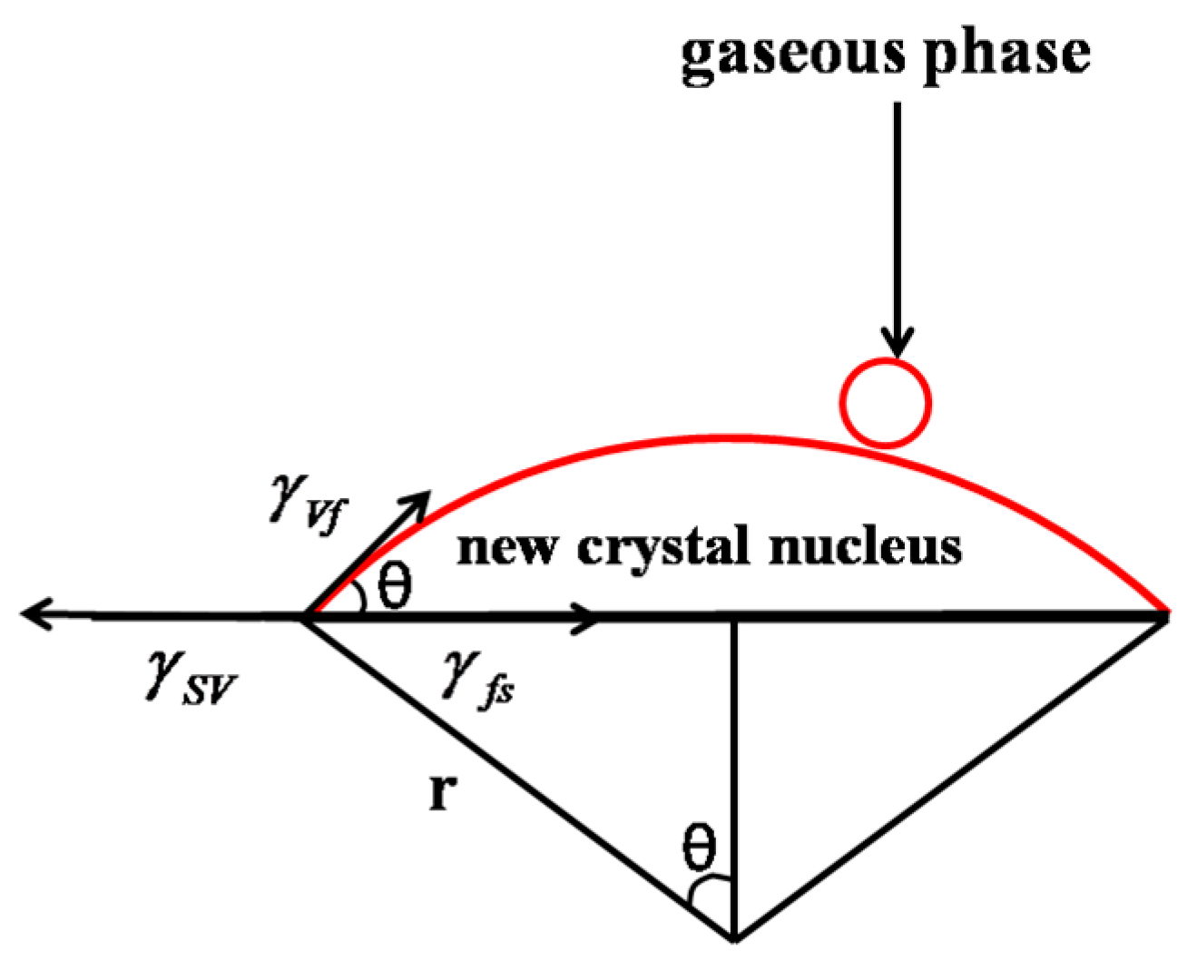
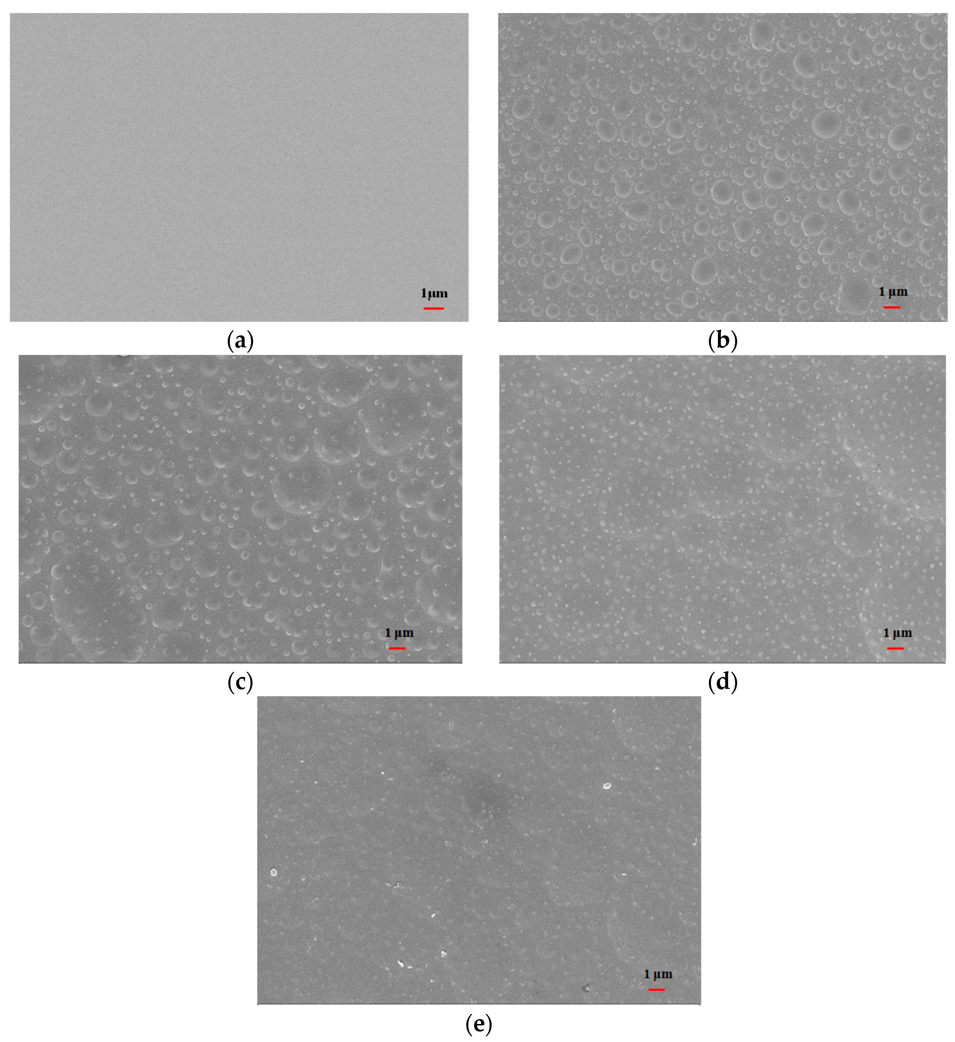
3.2. Film Growth and Surface Morphology

Through combining surface morphology and EDS investigation of the Al2O3 films in the first 10 min deposition, the growth process of Al2O3 films on n-InP substrates will be discussed (as shown in Figure 4a–g). Agglomerated islands are seen arranged randomly on the surface, and the EDS analysis of aluminum element content by comparing the island areas and the flat ones illustrated that there was much more aluminum in island areas than in the flat areas, suggesting that Al2O3 films initially grow in islands. This growth pattern was vividly displayed by comparing the AFM morphology of the bare n-InP substrate with that of the as-deposited Al2O3 film of 10 min deposition, as shown in Figure 4f,g.
During sputtering, the Al2O3 film would grow in a non-spontaneous nucleation mode. For one coronary crystal nucleus as illustrated in Figure 5, to assure the stable formation, its ΔG should follow the lowest energy principle, which can be formulated as follows [24]:
γ sv =   γ fs +   γ vf cos θ
where θ is the interface contact angle between the new nucleus and the substrate. When θ > 0, γ sv <   γ fs +   γ vf , the deposited film will grow in Volmer–Weber mode (island growth); when θ = 0, γ sv γ fs +   γ vf , the deposited film will grow in Frank–van der Merwe mode (layer-by-layer growth).
In this work, Al2O3 films deposited onto n-InP substrates first grew in Volmer–Weber mode, demonstrating that the wettability between them was poor and Al2O3 atoms more strongly bound to each other than to the n-InP substrate. Besides the different characteristics of the Al2O3 film and the InP substrate as two different kinds of materials, the following two factors were likely also responsible:
(1) The used n-InP substrates were polished and very smooth. Wentzel’s equation [25] is shown as follows:
cos θ R = W R cos θ 0
where θ R is the practical contact angle on a rough surface in equilibrium; WR is the ratio of the practical surface area and the nominal one; and θ 0 is the contact angle on an ideally smooth surface in equilibrium. This equation suggests that in the case of θ 0 < 90 0 , the practical contact angle becomes larger with smoother surface conditions and the wettability becomes poorer. In this study, we can tell that θ 0 < 90 0 , and the smooth n-InP substrate surface would be responsible for the poor wettability and lead to island growth of the deposited Al2O3 film.
(2) During sputtering, no intentional substrate heat treatment was done, and low substrate temperature means a short diffusion distance of those deposited atomic islands on the surface of the substrate, which is difficult for them to become connected to form a layer.
Figure 6 shows the surface morphology evolution of the as-deposited Al2O3 films with different deposition durations, perfectly interpreting the growth process of Al2O3 films. For reference, surface morphology of the bare n-InP substrate is displayed in Figure 6a and surface was smooth and clean. When the sputtering duration was 5 min, various-sized Al2O3 islands arranged randomly on the surface, as seen in Figure 6b. With the deposition time increased to 10 min (Figure 6c), big islands became larger and small ones were seen distributed among them. When the sputtering duration reached 20 min (Figure 6d), the larger islands showed further growth and became connected with each other. Notably, those connected islands were covered in superfine particles, meaning that the growth pattern of the sputtered Al2O3 film switched from the island mode to the layer-by-layer mode where film atoms become more strongly bound to the substrate than to each other. This could be attributed to the following three factors: (1) At this time, superfine Al2O3 particles were sputtered onto those connected Al2O3 islands instead of n-InP substrates, and they are identical materials; (2) the substrate surface was covered in large connected Al2O3 islands, and its surface roughness increased, leading to better wettability according to Wentzel’s equation; and (3) no intentional substrate heat treatment during sputtering meant those sputtered superfine particles could not possess enough kinetic energy to diffuse on the substrate to become agglomerated. When the sputtering duration was finally elevated to 40 min (Figure 6e), more particles were deposited onto the superfine-particle-dispersed surface. Continuous, compact, and uniform Al2O3 film was obtained on the n-InP substrate.

3.3. Optical and Dielectric Properties

Optical properties of the as-deposited Al2O3 films with a 40 min deposition duration were studied (Figure 7a,b). The mean transmittance of the film at wavelengths ranging from 200 to 2000 nm, was about 80%, which is higher than reported elsewhere [26], as a result of its ultrathin film thickness. In addition, the as-deposited Al2O3 film was amorphous (Figure 3). Its optical band gap could be estimated using a graph of (αhν)1/2 versus hν according to Tauc’s theory as shown in Figure 7b [27], where α, the optical attenuation coefficient at energy hν, is extracted from the transmittance spectra using the relation [28] α = ( 1 / d ) ln T film , where d is the film thickness, which was approximately 40 nm. From Figure 7b, the optical band gap of the Al2O3 film was found to be 3.72 eV, which was much lower than bulk Al2O3 (8.7 eV) [29] and the Al2O3 film prepared by spray pyrolysis [30], probably because defect energy levels formed in the energy band structure [31]. At a wavelength of 1550 nm, the optical attenuation coefficient (α) was calculated to be 3.0 × 104 cm−1, which is higher than that found by Shamala [32] in which the thickness of Al2O3 films prepared by electron beam evaporation was about 100 nm. This high optical attenuation agreed well with the low optical band gap because the existence of defect energy levels in the band structure would improve the optical absorption of the Al2O3 film and increase its optical loss.
The permittivity and dielectric loss of the 40-min-deposited Al2O3 films as a function of the frequency ranging from 100 Hz to 1 MHz are plotted in Figure 7c,d. With an increase in frequency, permittivity and dielectric loss both decreased and then became stable. When the frequency was 1 MHz, the permittivity was 8.96, which is in good agreement with Segda [33] in which Al2O3 films were also prepared by RF magnetron sputtering. However, the dielectric loss at a frequency of 1 MHz was 0.31 in this work, which was higher than those Al2O3 films prepared by the sol-gel method [34]. This is probably because numerous defects existed in the as-deposited Al2O3 film, and ions in the vicinity of these defects were weakly bonded and more easily activated. When the film was placed in an electric field, those ions around the defects would form conducting electricity and cause a large dielectric loss [32].
The impedance and its corresponding Nyquist spectrum of the 40-min-deposited Al2O3 films is shown in Figure 7e,f. From this, the resistivity of the film is 5 × 10¹⁰ Ω·cm, which is lower than reported elsewhere [1]. Such low resistivity is in accordance with the low optical band gap and the high dielectric loss of the as-deposited Al2O3 films, all of which stemmed from the numerous defects that probably existed in the as-deposited ultrathin film. Thus, intentional substrate heat treatment and post-deposition annealing would be expected to further optimize the deposited films and improve their corresponding properties in the future.

4. Conclusions

In this work, ultrathin Al2O3 films were fabricated onto n-InP substrates by RF magnetron sputtering to explore their candidacy for insulating layers in semiconductor lasers for optical communication. The as-deposited Al2O3 film was amorphous and near stoichiometric. It first grew in island mode, and when those islands became connected, it turned grew in layer-by-layer mode, because of the poor wettability between the Al2O3 film and the n-InP substrate, the smooth surface of the n-InP substrate, and the low deposition temperature. Compact and uniform Al2O3 films were obtained when the deposition duration reached 40 min. The mean transmittance, optical band gap, and the optical attenuation coefficient at a wavelength of 1550 nm of this A2O3 film were ~80%, 3.72 eV, and 3.0 × 104 cm−1, respectively. The permittivity and dielectric loss at a frequency of 1 MHz was 8.96 and 0.31, respectively, and the film resistivity was estimated to be 5 × 10¹⁰ Ω·cm. Though there is plenty of room to improve the optical and dielectric properties of the fabricated ultrathin Al2O3 film by RF magnetron sputtering, this work provides valuable references for ultrathin Al2O3 films applied in semiconductor lasers as candidate insulating layers to reduce the cost of device fabrication and simplify the fabrication process.

Author Contributions

Conceptualization, J.Z.; methodology, X.T.; data curation, Z.L. and H.L.; writing—original draft preparation, X.T.; writing—review and editing, J.Z.; supervision, J.Z.

Funding

This research was funded by National Youth Natural Science Foundation, grant number 51802229, Natural Science Foundation Of Guangdong Province, grant number 2018A030313561 and 2018A030313430, Innovation And Strong School Engineering Fund Of Guangdong Province, grant number 2016KQNCX169, 2017KQNCX197, and 2017 KQNCX201, Guangdong Natural Science Foundation For Distinguished Young Scholar, grant number, 2015A030306031, Science And Technology Projects Of Jiangmen, grant number, [2017] 307 and [2017] 149.

Conflicts of Interest

The authors declare no conflict of interest.

References

  1. Bartzsch, H.; Glöß, D.; Böcher, B.; Frach, P.; Goedicke, K. Properties of SiO2 and Al2O3 films for electrical insulation applications deposited by reactive pulse magnetron sputtering. Surf. Coat. Technol. 2003, 174, 774–778. [Google Scholar] [CrossRef]
  2. Aramesh, M.; Djalalian-Assl, A.; Yajadda, M.M.A.; Prawer, S.; Ostrikov, K. Thin nanoporous metal–insulator–metal membranes. ACS Appl. Mater. Interfaces 2016, 8, 4292–4297. [Google Scholar] [CrossRef]
  3. Nigro, R.L.; Schilirò, E.; Greco, G.; Fiorenza, P.; Roccaforte, F. Surface treatments on AlGaN/GaN heterostructures for gate dielectric Al2O3 thin films grown by atomic layer deposition. Thin Solid Film. 2016, 617, 138–142. [Google Scholar] [CrossRef]
  4. Tang, X.; Luo, F.; Ou, F.; Zhou, W.; Zhu, D.; Huang, Z. Effects of negative substrate bias voltage on the structure and properties of aluminum oxide films prepared by DC reactive magnetron sputtering. Appl. Surf. Sci. 2012, 259, 448–453. [Google Scholar] [CrossRef]
  5. Cueff, R.; Baud, G.; Benmalek, M.; Besse, J.; Butruille, J.; Jacquet, M. X-ray photoelectron spectroscopy studies of plasma-modified PET surface and alumina/PET interface. Appl. Surf. Sci. 1997, 115, 292–298. [Google Scholar] [CrossRef]
  6. Shih, K.K. Deposition of aluminum oxide films with high refractive index. J. Vac. Sci. Technol. A 1994, 12, 321–322. [Google Scholar] [CrossRef]
  7. Lin, H.C.; Yang, T.; Sharifi, H.; Kim, S.K.; Xuan, Y.; Shen, T.; Mohammadi, S.; Ye, P.D. Enhancement-mode GaAs metal-oxide-semiconductor high-electron mobility transistors with atomic layer deposited Al2O3 as gate dielectric. Appl. Phys. Lett. 2007, 91, 212101. [Google Scholar] [CrossRef]
  8. Poodt, P.; Lankhorst, A.; Roozeboom, F.; Spee, K.; Maas, D.; Vermeer, A.; Spee, C. High-speed spatial atomic-layer deposition of aluminum oxide layers for solar cell passivation. Adv. Mater. 2010, 22, 3564–3567. [Google Scholar] [CrossRef] [PubMed]
  9. Chen, X. Design of plasmonic-semiconductor nano-resonator lasers, geometrical energy velocity, and laser output-coupler optimization. Ph.D. Thesis, Northwestern University, Evanston, IL, USA, 2012. [Google Scholar]
  10. Zhu, L.; Liu, Y.; Zhang, H.; Xiao, H.; Guo, L. Atomic layer deposited Al2O3 films for anti-reflectance and surface passivation applications. Appl. Surf. Sci. 2014, 288, 430–434. [Google Scholar] [CrossRef]
  11. Von Gastrow, G.; Alcubilla, R.; Ortega, P.; Yli-Koski, M.; Conesa-Boj, S.; I Morral, A.F.; Savin, H. Analysis of the atomic layer deposited Al2O3 field-effect passivation in black silicon. Sol. Energy Mater. Sol. Cells 2015, 142, 29–33. [Google Scholar] [CrossRef]
  12. George, S.M. Atomic layer deposition: An overview. Chem. Rev. 2010, 110, 111–131. [Google Scholar] [CrossRef]
  13. Cuevas, A.; Li, T.-T.; Li, T. Effective surface passivation of crystalline silicon by RF sputtered aluminum oxide. Phys. Status Solidi RRL Rapid Res. Lett. 2009, 3, 160–162. [Google Scholar]
  14. Compaan, A.D.; Gupta, A.; Lee, S.; Wang, S.; Drayton, J. High efficiency, magnetron sputtered CdS/CdTe solar cells. Sol. Energy 2004, 77, 815–822. [Google Scholar] [CrossRef]
  15. Shimanovich, D.L.; Vorobjova, A.I.; Tishkevich, D.I.; Trukhanov, A.V.; Zdorovets, M.V.; Kozlovskiy, A.L. Preparation and morphology-dependent wettability of porous alumina membranes. Beilstein J. Nanotechnol. 2018, 9, 1423–1436. [Google Scholar] [CrossRef] [Green Version]
  16. Li, T.-T.A.; Ruffell, S.; Tucci, M.; Mansoulie, Y.; Samundsett, C.; De Iullis, S.; Serenelli, L.; Cuevas, A. Influence of oxygen on the sputtering of aluminum oxide for the surface passivation of crystalline silicon. Sol. Energy Mater. Sol. Cells 2011, 95, 69–72. [Google Scholar] [CrossRef]
  17. Cremer, R.; Witthaut, M.; Neuschütz, D.; Erkens, G.; Leyendecker, T.; Feldhege, M. Comparative characterization of alumina coatings deposited by RF, DC and pulsed reactive magnetron sputtering. Surf. Coat. Technol. 1999, 120, 213–218. [Google Scholar] [CrossRef]
  18. Ha, W.; Choo, M.; Im, S. Electrical properties of Al2O3 film deposited at low temperatures. J. Non-Cryst. Solids 2002, 303, 78–82. [Google Scholar] [CrossRef]
  19. Garcıa-Serrano, J.; Galindo, A.G.; Pal, U. Au–Al2O3 nanocomposites: XPS and FTIR spectroscopic studies. Sol. Energy Mater. Sol. Cells 2004, 82, 291–298. [Google Scholar] [CrossRef]
  20. Sun, C.; Zeng, R.; Zhang, J.; Qiu, Z.J.; Wu, D. Effects of UV-Ozone treatment on sensing behaviors of EGFETs with Al2O3 sensing film. Materials 2017, 10, 1432. [Google Scholar] [CrossRef] [PubMed]
  21. Afify, N.D.; Dalba, G.; Koppolu, U.M.K.; Armellini, C.; Jestin, Y.; Rocca, F. XRD and EXAFS studies of HfO2 crystallisation in SiO2–HfO2 films. Mater. Sci. Semicond. Process. 2006, 9, 1043–1048. [Google Scholar] [CrossRef]
  22. Takagi, A.; Nomura, K.; Ohta, H.; Yanagi, H.; Kamiya, T.; Hirano, M.; Hosono, H. Carrier transport and electronic structure in amorphous oxide semiconductor, a-InGaZnO4. Thin Solid Film. 2005, 486, 38–41. [Google Scholar] [CrossRef]
  23. Grover, M.S.; A Hersh, P.; Chiang, H.Q.; Kettenring, E.S.; Wager, J.F.; A Keszler, D. Thin-film transistors with transparent amorphous zinc indium tin oxide channel layer. J. Phys. D Appl. Phys. 2007, 40, 1335–1338. [Google Scholar] [CrossRef]
  24. Lüth, H. Solid Surfaces, Interfaces and Thin Films; Springer Nature: Aachen, Germany, 2010. [Google Scholar]
  25. Wenzel, R.N. Resistance of solid surfaces to wetting by water. Ind. Eng. Chem. 1936, 28, 988–994. [Google Scholar] [CrossRef]
  26. Khanna, A.; Bhat, D.G. Nanocrystalline gamma alumina coatings by inverted cylindrical magnetron sputtering. Surf. Coat. Technol. 2006, 201, 168–173. [Google Scholar] [CrossRef]
  27. Tauc, J.; Grigorovici, R.; Vancu, A. Optical properties and electronic structure of amorphous germanium. Phys. Status Solidi b 1966, 15, 627–637. [Google Scholar] [CrossRef]
  28. Prathap, P.; Subbaiah, Y.; Devika, M.; Reddy, K.R. Optical properties of In2O3 films prepared by spray pyrolysis. Mater. Chem. Phys. 2006, 100, 375–379. [Google Scholar] [CrossRef]
  29. Hu, B.; Yao, M.; Xiao, R.; Chen, J.; Yao, X. Optical properties of amorphous Al2O3 thin films prepared by a sol–gel process. Ceram. Int. 2014, 40, 14133–14139. [Google Scholar] [CrossRef]
  30. Adamopoulos, G.; Thomas, S.; Bradley, D.D.; McLachlan, M.A.; Anthopoulos, T.D. Low-voltage ZnO thin-film transistors based on Y2O3 and Al2O3 high-k dielectrics deposited by spray pyrolysis in air. Appl. Phys. Lett. 2011, 98, 123503. [Google Scholar] [CrossRef]
  31. Costina, I.; Franchy, R. Band gap of amorphous and well-ordered Al2O3 on Ni3Al (100). Appl. Phys. Lett. 2011, 78, 4139. [Google Scholar] [CrossRef]
  32. Shamala, K.; Murthy, L.; Rao, K.N. Studies on optical and dielectric properties of Al2O3 thin films prepared by electron beam evaporation and spray pyrolysis method. Mater. Sci. Eng. B 2004, 106, 269–274. [Google Scholar] [CrossRef]
  33. Segda, B.; Jacquet, M.; Besse, J. Elaboration, characterization and dielectric properties study of amorphous alumina thin films deposited by r.f. magnetron sputtering. Vacuum 2001, 62, 27–38. [Google Scholar] [CrossRef]
  34. Hu, B.; Yao, M.; Yang, P.; Shan, W.; Yao, X. Preparation and dielectric properties of dense and amorphous alumina film by sol–gel technology. Ceram. Int. 2013, 39, 7613–7618. [Google Scholar] [CrossRef]
Figure 1. Cross-sectional scanning electron micrograph (SEM) of the as-deposited Al2O3 film on a n-InP substrate when the deposition time is 20 min. Small figures on the right are the corresponding counterparts in the red circle.
Coatings 09 00341 g001
Figure 2. X-ray photoelectron spectra (XPS) analysis of the as-deposited Al2O3 film on a SiO2 substrate when the deposition duration was 20 min: (a) Al 2p; (b)O 1s.
Coatings 09 00341 g002
Figure 3. X-ray diffraction (XRD) spectra of the as-deposited and the 450 °C-annealed Al2O3 films on SiO2 substrates.
Coatings 09 00341 g003
Figure 4. Energy dispersive spectroscopy (EDS) analysis of the as-deposited Al2O3 films on n-InP substrates when the deposition durations were 5 min and 10 min: (a,b) 5 min as-deposited; (c,d) 10 min as-deposited; (e) atomic % of Al in the tested spots. Atomic force microscopy (AFM) morphologies of (f) a bare n-InP substrate and (g) of the as-deposited Al2O3 film on the n-InP substrate with a deposition duration of 10 min.
Coatings 09 00341 g004aCoatings 09 00341 g004b
Figure 5. Illustration of non-spontaneous nucleation of one crystal nucleus during film sputtering.
Coatings 09 00341 g005
Figure 6. Surface morphology evolution of as-deposited Al2O3 films on n-InP substrates with different deposition durations: (a) bare n-InP substrate for reference; (b) 5 min; (c) 10 min; (d) 20 min; and (e) 40 min.
Coatings 09 00341 g006
Figure 7. Optical and dielectric properties of the as-deposited Al2O3 film on a SiO2substrate with the deposition duration of 40 min:(a) transmittance; (b) optical band gap; (c) permittivity; (d) dielectric loss; (e) impedance; and (f) its Nyquist spectrum.
Coatings 09 00341 g007

