Abstract
In this paper, the correlation of impedance matching and optical emission spectroscopy during plasma-enhanced chemical vapor deposition (PECVD) was systematically investigated in SiH4 plasma diluted by various hydrogen dilution ratios. At the onset of nanocrystallinity in SiH4− depleted plasma condition, the SiH+ radical reached a threshold value as the dominant radical, such that a-Si to nc-Si transition was obtained. Furthermore, the experimental data of impedance analysis showed that matching behavior can be greatly influenced by variable plasma parameters due to the change of various hydrogen dilution ratios, which is consistent with the recorded optical emission spectra (OES) of Hα* radicals. Quadruple mass spectrometry (QMS) and transmission electron microscopy (TEM) were employed as associated diagnostic and characterization tools to confirm the phase transformation and existence of silicon nanocrystals.
1. Introduction
Compared to the hydrogenated amorphous silicon (a-Si:H), nano-crystalline silicon (nc-Si:H) films exhibit outstanding properties in terms of tailorable band-gap [1] and higher carrier mobility [2,3], and are possibly capable of boosting the conversion efficiency of silicon-based thin film solar cells [4,5].
In order to promote phase transition from a-Si:H to nanocrystallization of the nc-Si:H thin films, the plasma-assisted chemical vapor deposition (PECVD) system is widely used [6,7]. Processing parameters of argon dilution [8,9], deposition pressure [10], power density [11], SiH4 flow [12], temperature [13], ratio of H2/SiH4 [14], excitation frequency [15], and electrode separation [16] have been investigated. In addition, SiH radicals have a crucial influence on nc-Si deposition [17].
In order to characterize the transition zone and film properties of the PECVD deposition process, the utilization of plasma diagnostic tools is a crucial step that includes optical emission spectroscopy etc. [18,19,20]. Furthermore, threshold ionization mass spectrometry (TIMS) is an important tool for optimizing PECVD processes [21] with relative densities of ground-state source radicals and their evolution with hydrogen input [22]. In addition, film characterization tools such as Raman spectroscopy are invaluable to investigate the inherent structure [23,24] and predict the phase transition due to emission radicals at 520 cm−1 spectrum [25], which is assigned to the transversal optical (TO) mode of crystal grains of different sizes and whose significance regarding phase transition in the Raman spectrum showed that the optical mode of crystalline silicon located at ~520 cm−1 was primarily attributed to the quantum-sized confinement of phonons in nanocrystallites [26,27].
During the PECVD deposition process, the impedance analyzer can also be simultaneously conducted for predicting the plasma conditions of the critical point of transition [28]. One particularly useful tool for monitoring the impedance matching is the Smith chart (graphical impedance chart) [29]. The Smith chart can be used to find a lossless transmission-line for desired impedance matching [30,31].
The PECVD-deposited material quality in terms of plasma-based characterizations has been previously carried out by our group [14,32,33]. In this paper, the investigation of deposition processing parameters on plasma impedance and structurally evolved properties was studied simultaneously by the plasma diagnostic tools and impedance analyzer.
2. Experimental
2.1. Film Preparation
Intrinsic hydrogenated nanocrystalline silicon (nc-Si:H) thin films were deposited by plasma-enhanced chemical vapor deposition (PECVD) with RF power frequency 13.56 MHz (PE-001; Creating Nano-Technologies, Tainan City, Taiwan). PECVD equipment is indigenously designed and locally fabricated. Silane (SiH4) was used. The substrate temperature was fixed at ~210 °C. The detailed processing parameters can be listed as follows: power 100 W; pressure 300 mTorr; source gas: SiH4, H2, and Ar; SiH4 gas-flow 5 sccm; Ar gas-flow 3 sccm; H2 gas-flow can be varied as 25, 50, 100, 150, or 200 sccm; deposition time 60 min; electrode distance 25 mm; and substrate temperature 210 °C. Hydrogen dilution ratio is defined as the ratio between the hydrogen flow-rate divided by the silane flow-rate (R = H2/SiH4), which is the same definition as investigated previously in PECVD nc-Si:H films [14]. The substrate of CZ(100) n-type single-side polished wafer was used for all the experiments. The wafers were initially cleaned in a procedure that involved acid cleaning with H2O2:H2SO4 = 1:2 solutions for 5 min, 2% HF dipping for 1 min to remove native oxide, and the use of a load-lock chamber prior to each deposition to prevent oxygen contamination. Experimentally, processing parameter of hydrogen dilution ratio—R (R = 5–40)—was utilised and the associated plasma characteristics were monitored simultaneously via the diagnostic tools. In particular, the improved process stability on an extremely thin silicon interface passivation layer had been validated via the optimal predeposition time on the chamber wall [32], such that the chamber conditions were well maintained before each dilution experiment. In addition, the substrate holder and deposition chamber were thermally baked for two hours at 210 °C to prevent any water vapor and oxygen contamination.
2.2. Film Characterization
In order to quantitatively characterize the deposited films, various tools such as quadruple mass spectrometry (QMS, PSM003P, Hiden, Warrington, UK), optical emission spectroscopy (OES, usb2000+, Ocean Optics, Winter Park, CO, USA), threshold ionization mass spectrometry (TIMS, PSM003P, Hiden), and transmission electron microscopy (TEM, JEM2000FXⅡ, JEOL, Tokyo, Japan) were used. In addition, Zscan (3155135-003E, Advanced Energy, Fort Collins, CO, USA) primarily observed the effect of impedance matching time on the plasma discharge intensity.
3. Results and Discussion
3.1. Optical Emission Spectra Spectroscopy Analysis
In order to study the plasma characteristics such as the relative radical concentration of SiH*, Hα, etc., we initially examine the spectra of spatially resolved optical emission spectra (OES) measurements. Figure 1a shows OES spectra of ignition step correlated with the parameter R, indicating the stable plasma can be well maintained during the deposition process, irrespective of the values of dilution ratio. The duration of ignition step in Figure 1a varies depending on the dilution ratio and zoomed in Figure 1b, which shows the results of both automatic and manual tuning, respectively. The matching results can be closely correlated to the matching progress and will be described in Section 3.4 later. In addition, all the deposition parameters in the ignition step are the same as those in the main deposition step, except for the dilution ration R. Figure 1b shows transient behavior in the initial 15 s of the recorded time-resolved signal for Hα intensity, which will be later compared with the impedance matching results. After the plasma ignition step, a relatively stable and steady-state intensity was observed such that a gradual rise in intensity occurred with increase of dilution ratio during the initial 15–20 s. Figure 1c shows the OES plasma characteristics. The main excited radicals are SiH* (414.30 nm), Hβ (486.10 nm), Hα (656.30 nm), and Ar* (750.30 nm), which can be experimentally observed and associated with the electronically collided dissociation of SiH4 source gas. In fact, all cases of dilution ratio in this investigation can be automatically tuned, at a duration of 1–3 min. However, due to the time requirement from a stability concern, the auto-tune time was set below 4.5 s. The manual tuning required to reach matching is approximately 12 s, as recorded from Figure 1b. The reason that these three dilution ratios (R = 10, 30, and 40) needed to be manually tuned may be partially attributed to the significantly different plasma composition of the electron collision and dissociative excitation of SiH4 source gas. Furthermore, the various tuning algorithms from the matching box were considered to be highly classified and patented technology. A previous study also demonstrated that both the crystallization rate index (Hα*/SiH*) and the electron temperature (Si*/SiH*) increase in proportion to the increase of the dilution ratio [14]. Furthermore, quadruple mass spectra (QMS)-measured results indicated the radicals SiHx (0 < x < 4) reached various critical points of relative densities since the dilution ratio changes due to the different depletion level of silane radicals [14].
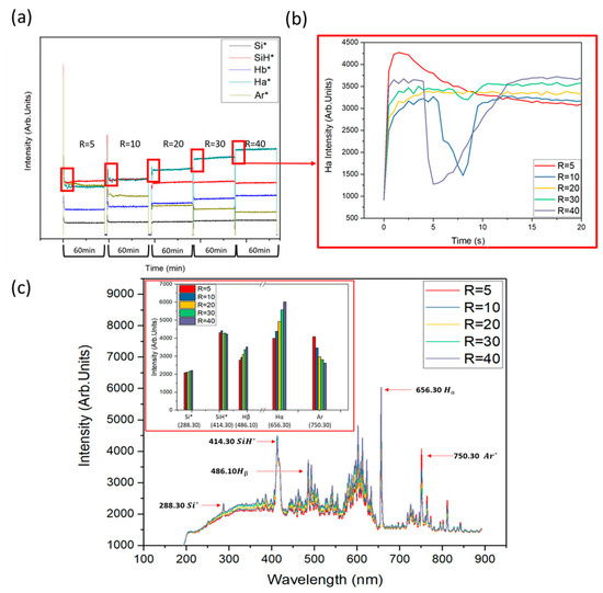
Figure 1.
(a) Time sequence of Si*, SiH*, and Hα* by optical emission spectra (OES)-resolved measurement; (b) Transient behavior of the initial 20 s of OES intensity for Hα intensity; and (c) Characteristics of OES.
3.2. Transmission Electron Microscopy
Transmission electron microscopy (TEM) images of the films deposited under R = 40 were prepared to validate the phase transformation of nanocrystalline grains. A large amount randomly distributed nanocrystal grains (dark regions) can be observed in Figure 2a. The inset shows the corresponding diffraction pattern, indicating the clear diffraction rings corresponding to Si <111>, Si <221>, and Si <311> from inside to outside, respectively. In addition, Figure 2b shows the discernably well-defined c-Si planes in <111> and <221> orientations. The effect of different hydrogen dilution ratio (R) along with Si <111>, Si <221>, and Si <311> orientations of nc-Si:H thin films has been analyzed by previous XRD spectra [14]. The effect of different hydrogen dilution ratio (R) can be analyzed by XRD spectra, as shown in Figure 3. X-ray diffraction (XRD) (APEX II, Bruker, Billerica, MA, USA; X-ray wavelength is 0.154 nm) was utilized to investigate the crystalline structure and crystal orientation. The diffraction patterns were obtained in the 2θ model (Bragg-Brentano configuration) with incident angle (2θ), with a glancing angle in the range of 20°–60°. Experimental results indicated that at a comparatively lower hydrogen dilution ratio in the range of R = 5–20, there is no visible diffraction peak at <111> crystallographic planes (2θ ~28.6°), indicating the amorphous films. In contrast, as the hydrogen dilution ratio increased to R = 30–40, a discernable <111> diffraction peak was observed in conjunction with the relatively weak peaks of <221> and <311>, respectively (2θ ~47.25° and ~56.1°), validating the occurrence of amorphous to crystalline phase transition, as evidenced in a previous study [14].
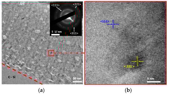
Figure 2.
Transmission electron microscopy (TEM) micrograph of nanocrystalline grains as prepared (R = 40) (a) and the related diffraction patterns (inset) (b).
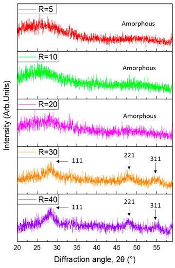
Figure 3.
Low-angle X-ray diffraction (XRD) pattern of plasma-enhanced chemical vapor deposition (PECVD) deposited nc-Si:H films.
3.3. Quadruple Mass Spectra
Residual gas analysis (RGA) was performed to evaluate plasma composition in the mass range 0–70 amu, as shown in Figure 4a. The main silane radicals such as SiH3*, SiH2+, SiH+, and Si+ (31–28 amu) were selectively observed, to evaluate their respective contribution to film growth. Figure 4b shows the TIMS-measured results of four mono-silane radicals (SiH3+, SiH2+, SiH+, and Si+). The detail calculation of Raman spectroscopy analysis and relevant transformation (a-Si to nc-Si) of quantitative structural information on the deposited thin films is similar to the previous study [14] such that the Levenberg–Marquardt method [14] was used to evaluate the crystalline fraction (XRaman) [34]. Figure 5 shows the Raman spectra of Si:H films deposited at different hydrogen dilution ratios (R). In particular, typical de-convoluted Raman spectra for a hydrogen dilution ratio of 40 is shown in Figure 5. The volume fraction of crystallites and crystallite size was evaluated as follows. Crystalline fraction (XRaman) can be calculated using Equation (1) [35]:
where Ic is the integrated intensity of the crystalline phase near 520 cm−1, Im is the integrated intensity of the intermediate phase around 500 cm−1, and Ia is the integrated intensity of the amorphous phase at 480 cm−1. The crystallite size (dRaman) was deduced using Equation (2):
where ∆ω is the peak shift compared to c-Si peak located ~520 cm−1 and β = 2.0 cm−1 nm2 [36].
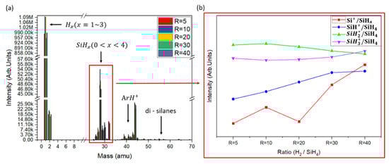
Figure 4.
(a) Residual gas analysis (RGA) mass scan; (b) Threshold ionization mass spectrometry (TIMS) relative SiHx (1 < x < 4) densities.
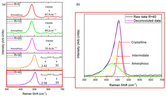
Figure 5.
(a) Raman spectra of PECVD deposited nc-Si:H films; (b) Gaussian de-convoluted Raman spectra at hydrogen dilution ratio (R = 40).
Based on the experimental results, the onset of nanocrystallization can be validated at a hydrogen dilution ratio of 30 as evidenced by XRaman ~31% and dRaman ~2.42 nm, which was theoretically originating from nanocrystalline phase [27]. Increasing the hydrogen dilution ratio to 40, XRaman and dRaman can be calculated as ~33% and ~2.58 nm, respectively. In summary, the hydrogen dilution ratio is deemed as an essential factor for the PECVD growth of nc-Si:H films [14]. PECVD deposition shows that the dominant SiH+ radical saturates at R ~30, such that a-Si to nc-Si transition can be obtained [34]. In the high silane dilution range of R = 30 and 40, QMS experiments confirmed that depletion of higher silane radicals can be of crucial importance to the existence of nano-crystalline phase [37,38].
3.4. Hydrogen Dilution Ratio Impact on the Matching Network
Impedance matching is of crucial importance in the RF source and transmission-line, such that the in-matching circuit can be power-transmitted with minimally reflected power. The matching box for the measured RF-driven PECVD power source is schematically shown in Figure 6a.
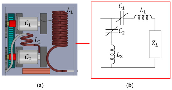
Figure 6.
(a) The matching box for the measured RF-driven PECVD power source; (b) The schematic equivalent circuit model of RF power transmission.
Considering the equivalent circuit of the RF-driven PECVD power source, the 13.56 MHz RF power supply can be modeled as RLC circuit is in a resonant state with 50 Ω characteristic impedance. As shown in Figure 6b, C1 and L1 are the primary parallel resonance circuit, and C2 and L2 are the secondary series resonance circuit. The suitable matching can be implemented via the adjustable capacitor C1 and C2. To further explore the complex plasma phenomenon and related dissociation behavior, the waveform of coupled RF power and Smith chart were experimentally monitored.
During the matching process, a load impedance range (Z = R + jX), composed of both resistive part and reactive parts, is required to prevent power losses. In theory, the voltage-current relationships for a lossless two-port network can be written as follows [39]:
In this study, the instantaneous matching behavior of plasma radio-frequency power amplifiers is of crucial importance primarily owing to high operating frequency (e.g., 13.56 MHz) and highly variable load parameters [40]. Therefore, Zscan equipment is used to measure the output power stabilization time and simultaneously compare it with OES measurement as well as the plasma discharge intensity. Figure 7a,b and Figure 8a–c show the time-resolved signal during plasma ignition as a function of R (R = H2/SiH4) and the tendency of forward power and reflected power in the RF energy source as presented in the Smith chart. Generally speaking, the stable plasma state can be generated with RF power at setting 100 W achieved to couple into the plasma, if the impedance matching can be achieved (as measured by Smith chart and OES spectra). In the matching case, the impedance of the matching unit was automatically or manually adjusted to approach 50 Ω, and pre-set 100 W can be coupled in the steady-state condition. Approximately 1 W RF power was reflected back to the RF generator.
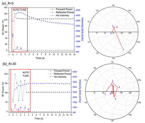
Figure 7.
The auto-tune results of RF power supply on the RF-positive power source: (a) R = 5; and (b) R = 20. Forward and reflected waveform of coupled RF power source (left) and associated Smith chart (right).
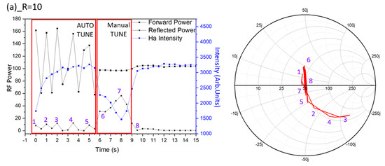
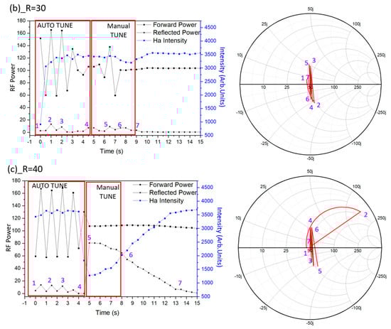
Figure 8.
The automatic and manual tune results of RF power supply on the RF-positive power source: (a) R = 10; (b) R = 30; and (c) R = 40. Forward and reflected waveform of coupled RF power source (left) and associated Smith chart (right).
As shown in Figure 7a,b, for the case of R = 5, the RF generator automatic matching (AUTO TUNE) can achieve load impedance matching with a small amplitude of oscillation and fast matching time (less than 4.5 s), and the plasma process quickly achieves stability with a variation of less than 1%. On the other hand, for the case of R = 20, the plasma process has a great impact on the internal resistance of the chamber, and therefore automatic matching (AUTO TUNE) falls into the unsettling mode with relatively significant oscillation amplitude before the final matching can be achieved (~4.5 s).
Figure 8a–c shows that the change in the internal resistance of the chamber makes the RF generator automatic matching (AUTO TUNE) fall into the unsettling mode (more than 4.5 s) with significant oscillation amplitude. Therefore, the chamber resistance cannot be matched to the optimum-state, such that manual matching (MANUAL TUNE) is required. Manual matching can be applied to the optimal matching condition based on previous settling points, such that the high transmitted power of 100 W with reflected power of less than 1 W can be experimentally achieved in three cases of hydrogen dilution ratio R = 10, 30, and 40, respectively.
Figure 9a–c showed the repeatability of impedance tuning at three different times and the related OES intensity at R = 20. The Smith chart showed a different matching path. The reason for these differences may be partially attributed to the initial chamber conditions and the associated complicated plasma condition involved. However, the matching algorithm can reach the optimal matching condition based on previous settling point such that the high transmitted power of 100 W with a reflected power of less than 1 W can be experimentally achieved.
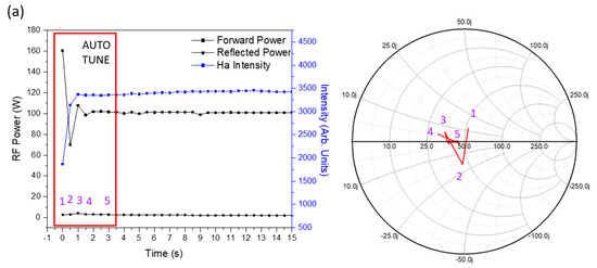
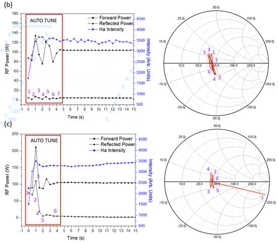
Figure 9.
The repeatability of impedance tuning and related OES intensities are performed for three times (a–c) at R = 20.
4. Conclusions
Real-time measurement of plasma properties was concurrently monitored by using the plasma diagnostic of OES for the radicals and the impedance probe for characterizing the hydrogen dilution ratio-induced plasma variation during the silicon thin films growth. OES data showed that the main excited radicals of SiH* (414.30 nm) can be experimentally observed and are associated with the electronic collision and dissociative excitation of SiH4 source gas. As the dilution ratio rises, both the crystallization rate index (Hα*/SiH*) and the electron temperature (Si*/SiH*) increase accordingly. TEM images confirmed the existence of nanocrystalline grains. For the impedance matching behavior, the Smith chart results show that for each dilution ratio, less than 1% of the reflected power within 9 s was achieved in either automatic or manual operation modes across the severely changing plasma range of operation.
Author Contributions
Conceptualization, T.T.L., Y.-K.F., and C.-C.L.; Methodology, Y.-L.H.; Software, L.-H.K. and H.-J.H.; Validation, Y.-L.H., L.-H.K., and H.-J.H.; Formal Analysis, Y.-L.H., L.-H.K., and H.-J.H.; Investigation, T.T.L. and Y.-K.F.; Curation, T.T.L., Y.-K.F., C.-C.L., and Y.-L.H.; Writing—Original Draft Preparation, Y.-K.F., T.T.L., L.-H.K., H.-J.H., and H.-E.C.; Writing—Review and Editing, Y.-K.F., T.T.L., L.-H.K., H.-J.H., and H.-E.C.; Visualization, L.-H.K. and H.-J.H.; Supervision, T.T.L., Y.-K.F., and C.-C.L.; Project Administration, T.T.L., Y.-K.F., and C.-C.L.
Funding
This research was financially funded by the Delta Electronics, Inc., Taiwan (No. 10613082).
Acknowledgments
This study was technically supported by Delta Electronics, Inc., Taiwan and Department of Mechanical Engineering, Optical Science Center and Department of Optics and Photonics, National Central University, Taiwan.
Conflicts of Interest
The authors declare no conflict of interest.
References
- Kitao, J.; Harada, H.; Yoshida, N.; Kasuya, Y.; Nishio, M.; Sakamoto, T.; Itoh, T.; Nonomura, S.; Nitta, S. Absorption coefficient spectra of μc-Si in the low-energy region 0.4–1.2 eV. Sol. Energy Mater. Sol. Cells 2001, 66, 245–251. [Google Scholar] [CrossRef]
- Shah, A.V.; Meier, J.; Vallat-Sauvain, E.; Wyrsch, N.; Kroll, U.; Droz, C.; Graf, U. Material and solar cell research in microcrystalline silicon. Sol. Energy Mater. Sol. Cells 2003, 78, 469–491. [Google Scholar] [CrossRef]
- Ito, M.; Koch, C.; Svrcek, V.; Schubert, M.B.; Werne, J.H. Silicon thin film solar cells deposited under 80 °C. Thin Solid Films 2001, 383, 129–131. [Google Scholar] [CrossRef]
- Guha, S.; Yang, J.; Yan, B. High efficiency multi-junction thin film silicon cells incorporating nanocrystalline silicon. Sol. Energy Mater. Sol. Cells 2013, 119, 1–11. [Google Scholar] [CrossRef]
- Green, M.A.; Emery, K.; Hishikawa, Y.; Warta, W.; Dunlop, E.D. Solar cell efficiency tables (version 46). Prog. Photovolt. Res. Appl. 2015, 23, 805–812. [Google Scholar] [CrossRef]
- Vallat-Sauvain, E.; Kroll, U.; Meier, J.; Shah, A. Evolution of the microstructure in microcrystalline silicon prepared by very high frequency glow-discharge using hydrogen dilution. J. Appl. Phys. 2000, 87, 3137. [Google Scholar] [CrossRef]
- Li, S.B.; Wu, Z.M.; Jiang, Y.D.; Li, W.; Liao, N.M.; Yu, J.S. Structure and 1/f noise of boron doped polymorphous silicon films. Nanotechnology 2008, 19, 085706. [Google Scholar] [CrossRef]
- Das, U.K.; Chaudhuri, P.; Kshirsagar, S.T. Effect of argon dilution on the structure of microcrystalline silicon deposited from silane. J. Appl. Phys. 1996, 80, 5389. [Google Scholar] [CrossRef]
- Das, D. Structural studies on Si:H network by Raman, micro-photoluminescence, electron microscopy and ultraviolet ellipsometry: Effect of Ar dilution to the SiH4-plasma. Thin Solid Films 2005, 476, 237–245. [Google Scholar] [CrossRef]
- Gope, J.; Kumar, S.; Singh, S.; Rauthan, C.M.S.; Srivastava, P.C. Growth of mixed-phase amorphous and ultra nanocrystalline silicon thin films in the low pressure regime by a VHF PECVD process. Silicon 2012, 4, 127–135. [Google Scholar] [CrossRef]
- Parashar, A.; Kumar, S.; Gope, J.; Rauthan, C.M.S.; Hashmi, S.A.; Dixit, P.N. RF power density dependent phase formation in hydrogenated silicon films. J. Non-Cryst. Solids 2010, 356, 1774–1778. [Google Scholar] [CrossRef]
- Gope, J.; Kumar, S.; Sudhakar, S.; Lodhi, K.; Rauthan, C.M.S.; Srivastava, P.C. Influence of argon dilution on the growth of amorphous to ultra nanocrystalline silicon films using VHF PECVD process. J. Alloy. Compd. 2013, 577, 710–716. [Google Scholar] [CrossRef]
- Hadjadj, A.; Beorchia, A.; Cabarrocas, P.R.; Boufendi, L.; Huet, S.; Bubendorff, J.L. Effects of the substrate temperature on the growth and properties of hydrogenated nanostructured silicon thin films. J. Phys. D Appl. Phys. 2001, 34, 690. [Google Scholar] [CrossRef]
- Hsieh, Y.L.; Kau, L.H.; Huang, H.J.; Lee, C.C.; Fuh, Y.K.; Li, T.T. In Situ plasma monitoring of PECVD nc-Si:H Films and the influence of dilution ratio on structural evolution. Coatings 2018, 8, 238. [Google Scholar] [CrossRef]
- Luysberg, M.; Hapke, P.; Carius, R.; Finger, F. Structure and growth of hydrogenated microcrystalline silicon: Investigation by transmission electron microscopy and Raman spectroscopy of films grown at different plasma excitation frequencies. Philos. Mag. A 1997, 75, 31–47. [Google Scholar] [CrossRef]
- Chowdhury, A.; Mukhopadhyay, S.; Ray, S. Effect of electrode separation on PECVD deposited nanocrystalline silicon thin film and solar cell properties. Sol. Energy Mater. Sol. Cells 2010, 94, 1522–1527. [Google Scholar] [CrossRef]
- Donne, A.L.; Binetti, S.; Isella, G.; Pichaud, B.; Texier, M.; Acciarri, M.; Pizzini, S. Structural characterization of nc-Si films grown by low-energy PECVD on different substrates. Appl. Surf. Sci. 2008, 254, 2804–2808. [Google Scholar] [CrossRef]
- Koirala, S.P.; Abu-Safe, H.H.; Mensah, S.L.; Naseem, H.A.; Gordon, M.H. Langmuir probe and optical emission studies in a radio frequency (rf) magnetron plasma used for the deposition of hydrogenated amorphous silicon. Surf. Coat. Technol. 2008, 203, 602–605. [Google Scholar] [CrossRef]
- Oda, S.; Noda, J.; Matsumura, M. Diagnostic study of VHF plasma and deposition of hydrogenated amorphous silicon films. Jpn. J. Appl. Phys. 1990, 29, 1889. [Google Scholar] [CrossRef]
- Sahu, B.B.; Han, J.G.; Shin, K.S.; Ishikawa, K.; Hori, M.; Miyawaki, Y. Plasma diagnostic approach for high rate nanocrystalline Si synthesis in RF/UHF hybrid plasmas using a PECVD process. Plasma Sources Sci. Technol. 2015, 24, 025019. [Google Scholar] [CrossRef]
- Cristophorou, L.G.; Olthoff, J.K. Fundamental electron-molecule interactions and their technological significance. In Fundamental Electron Interactions with Plasma Processing Gases; Springer: Boston, MA, USA, 2004; pp. 1–59. [Google Scholar]
- Kummer, M.; Rosenblad, C.; Dommann, A.; Hackbarth, T.; Höck, G.; Zeuner, M.; Muller, E.; Kanel, H. Low energy plasma enhanced chemical vapor deposition. Sci. Eng. B 2002, 89, 288–295. [Google Scholar] [CrossRef]
- Ferrara, M.A.; Donato, M.G.; Sirleto, L.; Messina, G.; Santangelo, S.; Rendina, I. Study of strain and wetting phenomena in porous silicon by Raman scattering. J. Raman Spectrosc. 2008, 39, 199–204. [Google Scholar] [CrossRef]
- Lee, N.; Hartschuh, R.D.; Mehtani, D.; Kisliuk, A.; Maguire, J.F.; Green, M.; Foster, M.D.; Sokolov, A.P. High contrast scanning nano-Raman spectroscopy of silicon. J. Raman Spectrosc. 2007, 38, 789–796. [Google Scholar] [CrossRef]
- Ehbrecht, M.; Kohn, B.; Huisken, F.; Laguna, M.A.; Paillard, V. Photoluminescence and resonant Raman spectra of silicon films produced by size-selected cluster beam deposition. Phys. Rev. B 1997, 56, 6958. [Google Scholar] [CrossRef]
- Hu, Z.; Liao, X.; Diao, H.; Cai, Y.; Zhang, S.; Fortunato, E.; Martins, R. Hydrogenated p-type nanocrystalline silicon in amorphous silicon solar cells. J. Non-Cryst. Solids 2006, 352, 1900–1903. [Google Scholar] [CrossRef]
- Li, Z.; Li, W.; Jiang, Y.; Cai, H.; Gong, Y.; He, J. Raman characterization of the structural evolution in amorphous and partially nanocrystalline hydrogenated silicon thin films prepared by PECVD. J. Raman Spectrosc. 2011, 42, 415–421. [Google Scholar] [CrossRef]
- Kroll, U.; Shah, A.; Keppner, H.; Meier, J.; Torres, P.; Fischer, D. Potential of VHF-plasmas for low-cost production of a-Si:H solar cells. Sol. Energy Mater. Sol. Cells 1997, 48, 343–350. [Google Scholar] [CrossRef]
- Smith, P.H. Transmission line calculator. Electronics 1939, 12, 29–31. [Google Scholar]
- Malherbe, J.A.G. The locus of points of constant VSWR when renormalized to a different characteristic impedance. IEEE Trans. Microw. Theory Tech. 1977, 25, 444–445. [Google Scholar] [CrossRef]
- Kurokawa, K. Power waves and the scattering matrix. IEEE Trans. Microw. Theory Tech. 1965, 13, 194–202. [Google Scholar] [CrossRef]
- Hsieh, Y.L.; Tseng, C.L.; Lee, C.C.; Fuh, Y.K.; Chang, J.Y.; Lee, J.Y.; Li, T.T. Improved process stability on an extremely thin amorphous/crystalline silicon interface passivation layer by using predeposition on the chamber wall. ECS J. Solid State Sci. Technol. 2018, 7, 355–361. [Google Scholar] [CrossRef]
- Hsieh, Y.L.; Kau, L.H.; Huang, H.J.; Lee, C.C.; Fuh, Y.K.; Li, T.T. In-situ plasma monitoring of PECVD a-Si:H (i)/a-Si:H (n) surface passivation for heterojunction solar cells application. In Proceedings of the 2018 China Semiconductor Technology International Conference (CSTIC), Shanghai, China, 11–12 March 2018. [Google Scholar]
- Kirner, S.; Gabriel, O.; Stannowski, B.; Rech, B.; Schlatmann, R. The growth of microcrystalline silicon oxide thin films studied by in situ plasma diagnostics. Appl. Phys. Lett. 2013, 102, 051906. [Google Scholar] [CrossRef]
- Chaudhary, D.; Sharma, M.; Sudhakar, S.; Kumar, S. Investigation of powder dynamics in silane-argon discharge using impedance analyser. Phys. Plasmas 2016, 23, 123704. [Google Scholar] [CrossRef]
- He, Y.; Yin, C.; Cheng, G.; Wang, L.; Liu, X.; Hu, G.Y. The structure and properties of nanosize crystalline silicon films. J. Appl. Phys. 1994, 75, 797. [Google Scholar] [CrossRef]
- Kondo, M.; Fukawa, M.; Guo, L.; Matsuda, A. High rate growth of microcrystalline silicon at low temperatures. J. Non-Cryst. Solids 2000, 266–269, 84–89. [Google Scholar] [CrossRef]
- Strahm, B.; Howling, A.A.; Sansonnens, L.; Hollenstein, C. Optimization of the microcrystalline silicon deposition efficiency. J. Vac. Sci. Technol. A 2007, 25, 1198. [Google Scholar] [CrossRef]
- Bastami, A.A.; Jurkov, A.; Gould, P.; Hsing, M.; Schmidt, M.; Ha, J.-I.; Perreault, D.J. Dynamic matching system for radio-frequency plasma generation. IEEE Trans. Power Electron. 2018, 33, 1940–1951. [Google Scholar] [CrossRef]
- Chaudhary, D.; Sharma, M.; Sudhaka, S.; Kuma, S. Effect of pressure on bonding environment and carrier transport of a-Si:H thin films deposited using 27.12 MHz assisted PECVD process. Silicon 2018, 10, 91–97. [Google Scholar] [CrossRef]
© 2019 by the authors. Licensee MDPI, Basel, Switzerland. This article is an open access article distributed under the terms and conditions of the Creative Commons Attribution (CC BY) license (http://creativecommons.org/licenses/by/4.0/).