1. Introduction
To improve the operation performance of integrated circuits (ICs), the dimensions of electronic devices are continuously being scaled-down to the deep submicron level. At this time, however, the interconnects-induced resistance-capacitance (RC) time delay is rapidly increasing, being a limiting factor for ICs performance [
1,
2,
3]. To reduce RC time delay, Cu metal and a low-dielectric-constant (low-
k) material are being used to replace the conventional Al metal and SiO
2 film in the back-end-of-line (BEOL) interconnects. Compared to Al metal (~2.82 μΩ-cm), Cu metal (~1.70 μΩ-cm) can provide a lower resistivity by approximately 35% [
4]. Low-
k materials with the dielectric constant (
k) lower than 3.9 (
k of SiO
2) can reduce the parasitic capacitance between metal lines [
5,
6]. Low-
k materials can be achieved by the introduction of lower polarization chemical bonds to replace Si–O bonds, but the reachable minimum
k-value is limited for this type of low-
k material, being 2.8. Therefore, to further reduce
k-value of low-
k materials, reducing the film’s density by introducing nanometer pores into the matrix of the existed low-
k material is another strategy. This is because air in the pore provides a minimum
k value (~1.0). The produced low-
k materials are porous, well-known as porous low-
k dielectrics [
6,
7]. Owing to the presence of pores, the porous low-
k dielectrics are mechanically and electrically weak, resulting in more challenges as they are integrated into BEOL interconnects [
8,
9].
Increasing porosity in the porous low-
k dielectrics favors to decrease
k-values, however, as the porosity reaches a critical value, the pores are open to the surface and connected internally. This provides a fast penetration pathway for gases, liquids, or other deposition precursors to enter the dielectric film, causing electrical characteristics and reliability of the porous low-
k dielectrics [
10,
11]. As a result, for the successful integration of highly porous low-
k dielectrics into the BEOL interconnects, pore-stuffing or pore-sealing processing is required as ways of plasma treatment, dielectric capping, or self-assembled monolayers (SAMs) [
12,
13,
14,
15].
Cu diffusing into the highly porous low-
k dielectric is an increasingly important issue. The barriers therefore are needed to confine Cu wires. Traditionally, the used metal barriers are Ti(N), Ta(N), or Ru(N) with a relatively high resistivity compared to Cu, thereby increasing line resistance for Cu metallization [
16,
17]. This situation is getting worse with scaling of BEOL interconnects because a large fraction of the line-width is occupied by the metal barrier. Decreasing the metal barrier thickness is a straightforward strategy to avoid a huge increase in the line resistance, but the loss of Cu barrier performance is a concern to be pay attention.
It therefore necessitates the development of a thin layer formed at the surface of highly porous low-
k dielectrics for sealing the pores and stopping Cu diffusion. The requirement of the formation layer is to minimize the increase of
k-value for highly porous low-
k dielectrics. SAMs have been proposed as a promising processing with sealing the pores and stopping Cu diffusion for highly porous low-
k dielectrics [
15]. With a very thin thickness (~<3 nm), SAMs have high compatibility with BEOL fabrication processes [
15,
18].
This study, therefore, proposes a process to form SAMs at the surface of highly porous low-k dielectrics (k = 2.25) by 3-Aminopropyltrimethoxysilane (APTMS; C6H17NO3Si) treatment in aqueous phase. The effects of the formation SAMs on the electrical characteristics and reliability of highly porous low-k dielectrics are evaluated. The barrier against Cu diffusion for the formation SAMs is investigated as well.
2. Experimental
The used highly porous low-
k materials in this study are SiOCH films with a
k value of 2.25, deposited on 300 mm p-type silicon wafers using plasma-enhanced chemical vapor deposition (PECVD, Applied Materials, Santa Clara, CA, USA) method [
19]. The average pore size and porosity of the resulting highly porous low-
k films are around 1.15 nm and 32.0%, respectively, which were determined from the isotherm of ethanol adsorption and desorption using ellipsometric porosimetry. The deposition thickness was controlled at 300 ± 10.0 nm, which was determined using an optical-probe system with an ellipsometer (Film Tek
TM 3000SE, High Point, NC, USA).
Then, the wafer was cleaved in 3 × 3 cm2 coupons and a thermal anneal at 200 °C for 1 min was performed to remove the adsorption moisture from the sample. The samples were immersed into a 85 °C SC-1 solution [deionized water: NH4OH (29%): H2O2 (28%) = 5:1:1], in an attempt to create active surface silanol functional groups. After immersion, the samples were rinsed thoroughly with deionized water and blown dry with a stream nitrogen gas. Following, the samples were immersed into the wet solution containing anhydrous toluene and 3-Aminopropyltrimethoxysilane (2.8 wt.%) for 1 h and 3 h at 70 °C in order to form SAMs at the surface of highly porous low-k dielectrics. Finally, a thermal anneal at 200 °C for 3 min was performed on the samples to remove the residues and moisture.
After the formation of SAMs on the highly porous low-k dielectrics, Cu film was deposited onto it to fabricate metal-insulator-silicon (MIS) capacitors for electrical characteristics and reliability measurements. Cu electrode in the MIS capacitor was prepared using a thermal evaporation method through a shadow mask. The formation thickness and area of Cu electrode were ~100 nm and 9.0 × 10⁻⁴ cm2, respectively. Capacitance–voltage (C–V), current–voltage (I–V), and time-dependent-dielectric-breakdown (TDDB) were characterized. C–V measurement was operated at the frequency of 1 MHz using a semiconductor parameter analyzer (HP4280A, Agilent technologies, Santa Clara, CA, USA). I–V measurement was made by sweeping the voltage and the response leakage current was monitored. TDDB measurement was tested in a fixed electric-field to record the failure time, in which the monitored leakage current suddenly increases by at least three-orders of magnitude. The I–V and TDDB measurements were performed using an electrometer (Keithley, 6517A, Austin, TX, USA). All measurements were performed at room temperature (25 °C).
In addition to electrical characterization, surface analyses were performed on the SAMs-formed samples. Water contact angle (WCA; Reme Hardt, Mode-100-00-230) was determined as the average of five measurements. Atomic force microscopy (AFM) was used to measure the surface morphology and root-mean-square (RMS) values. X-ray photoelectron spectroscopy (XPS; PHI 500, ULVAC-PHI, Inc., Chigasaki, Japanese), equipped with a monochromatized X-ray source of Al-Kα radiation (1486.6 eV), was used to analyze the changes in the surface structure of the porous low-k dielectrics before and after APTMS treatment.
3. Results and Discussion
The
k value of a dielectric film can be determined by means of the measured accumulation capacitance obtained from
C–V measurement, used in the expression of
k =
Cd/ε
0A. Here,
C is measured capacitance,
d is film thickness, and
A is the area of the device.
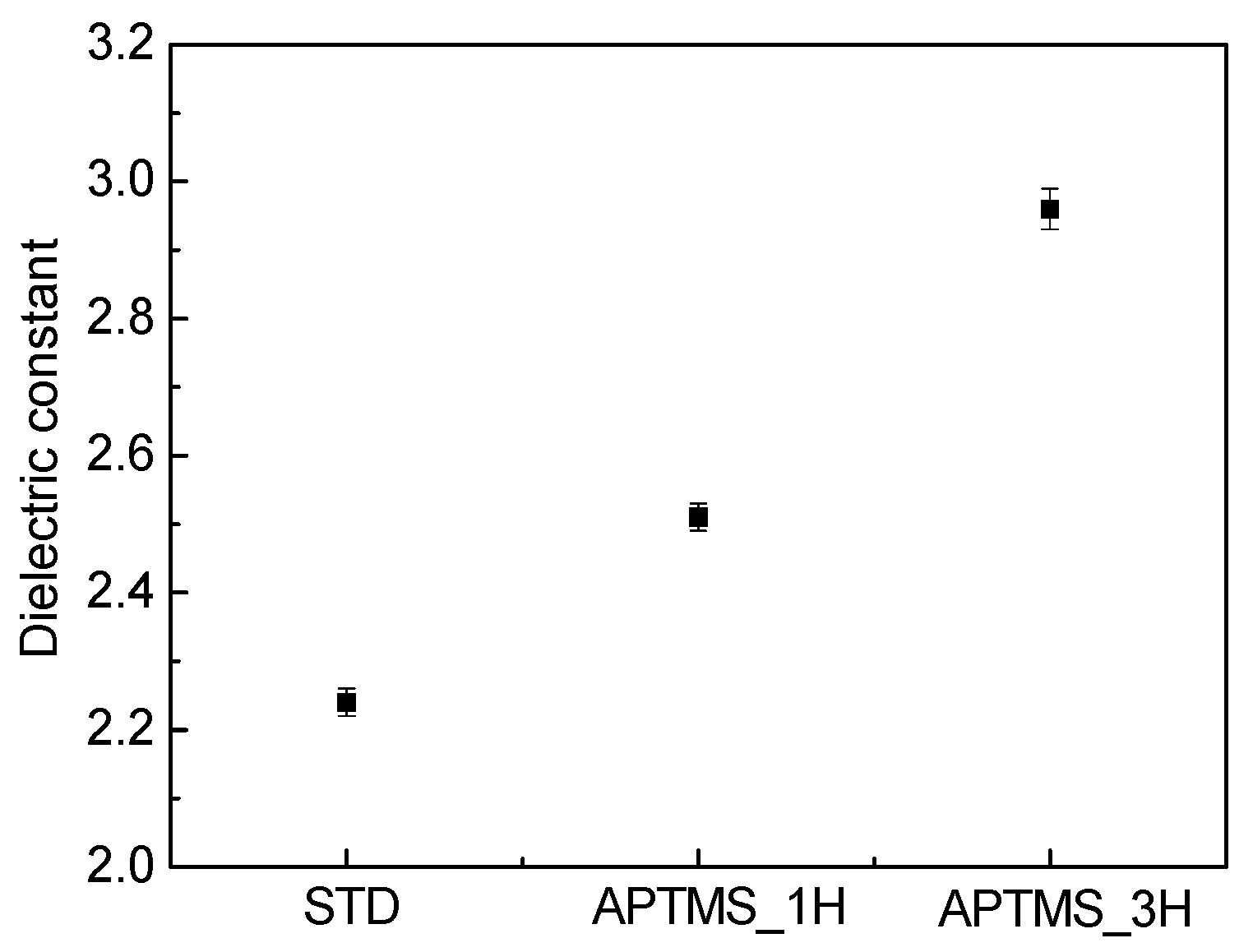
Figure 1 shows the determined
k values of the studied highly porous low-
k dielectrics before and after APTMS treatment. The results presented here are from 5 measurements on different MIS samples for each condition. The
k value of pristine highly porous low-
k dielectrics [donated as STD] was determined to be 2.25 ± 0.03. After APTMS treatment, the
k value increased and the increasing magnitude was amplified with the treatment time. The
k value of highly porous low-
k dielectrics with APTMS treatment for 3 h [donated as AMTMS_3H] reached 2.96 ± 0.04. An increased
k value can be attributed to the formation of SAMs on the surface of highly porous low-
k dielectrics.
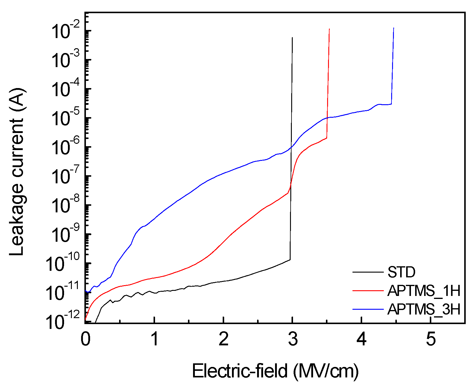
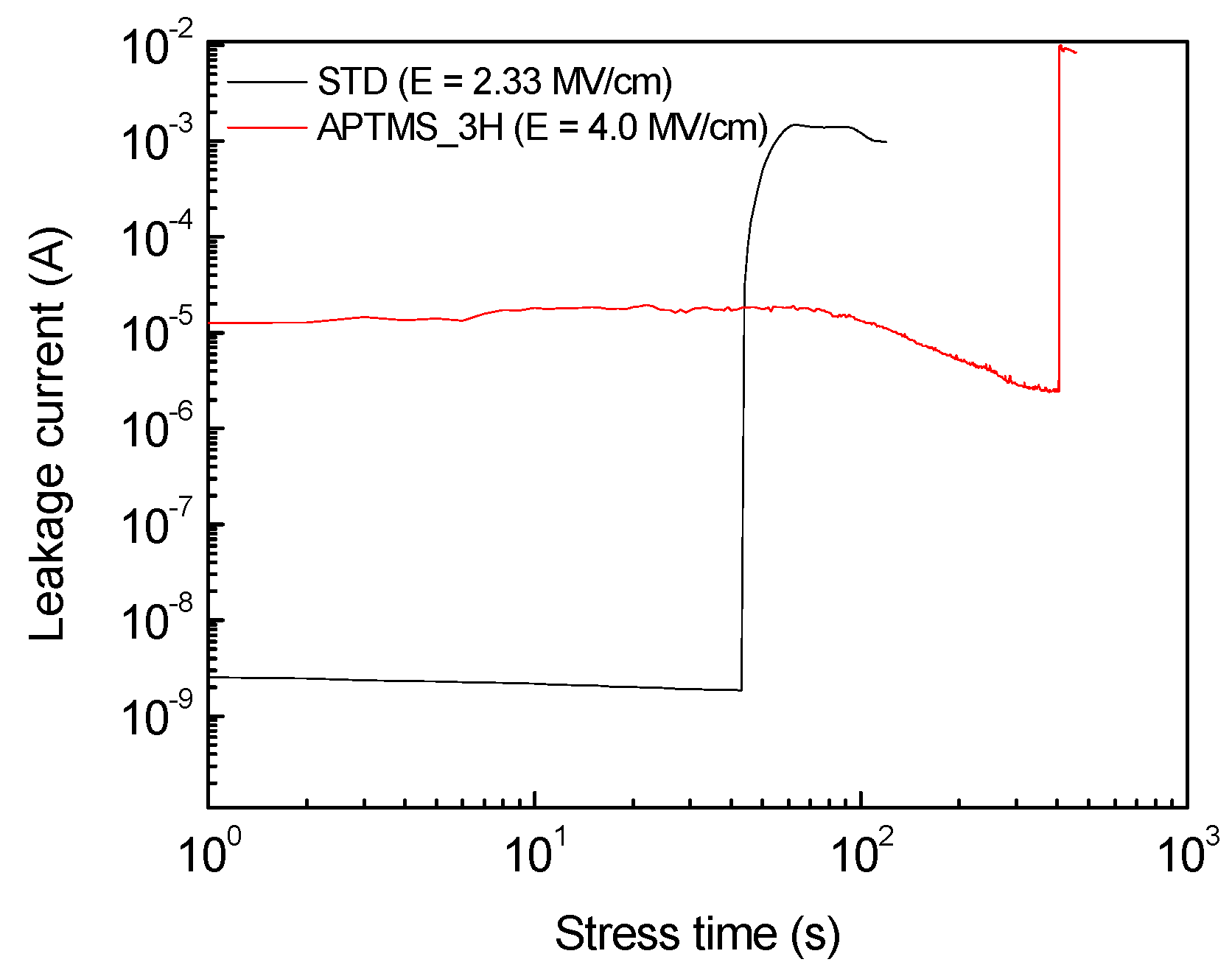
Figure 2 shows
I–E plots of highly porous low-
k dielectrics before and after APTMS treatment. By sweeping the voltage, the leakage current is monitored until breakdown. The breakdown is defined as the monitored leakage current suddenly increases at least three orders of magnitude. The electric-field was calculated by dividing the applied voltage by the thickness of highly porous low-
k dielectrics. The behavior of the leakage current versus the applied electric field of highly porous low-
k dielectrics was changed by APTMS treatment. The highly porous low-
k dielectrics with APTMS treatment displayed a faster increase in the leakage current than the samples without APTMS treatment. Additionally, a higher leakage current was detected as the highly porous low-
k dielectrics were immersed in APTMS solution with a longer immersion time. An increase in the leakage current for the APTMS solution-treated low-
k dielectrics is attributed to the top modification layer or the formation of SAMs, which is suspected to be a fast path for electron conduction due to the interface-dominated.
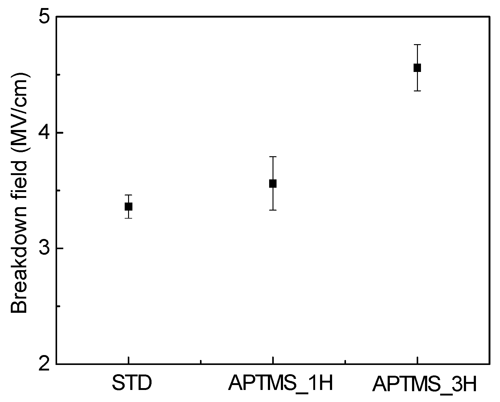
In contrast, the highly porous low-
k dielectrics after APTMS treatment exhibited an enhanced dielectric breakdown field. This enhancement was magnified with increasing the immersion time in APTMS solution, as shown in
Figure 3. The results were collected from ten samples for each condition. The average value and 3δ variation (error bar) were shown. The average breakdown field of highly porous low-
k dielectrics with APTMS treatment for 3 h was improved from 3.36 MV/cm (the breakdown field of the pristine sample) to 4.56 MV/cm. The opposite trend in the leakage current and breakdown field suggests that the leakage current is not a necessary condition to trigger the dielectric breakdown. A similar result was reported by Chen and Shinosky [
20]. Their data showed that the leakage current of Cu liner-free samples was much lower than that of with-Cu liner samples. However, the breakdown voltages of Cu liner-free samples were considerably lower than that of with-Cu liner samples. The unique electrical characteristics for APTMS-treated highly porous low-
k dielectrics may be attributed to Cu barrier and pore-sealing effects due to the formation SAMs [
21]. For the highly porous low-
k dielectrics without APTMS treatment, the diffused Cu ions during the deposition of Cu electrode can trap electrons to reduce the leakage current, however, they would accumulate to form a conduction path to accelerate the breakdown. Therefore, the formation SAMs on the highly porous low-
k dielectrics by APTMS treatment blocks Cu diffusion. Moreover, the opened-pores at the surface of the highly porous low-
k dielectrics are sealed, thus retarding the dielectric breakdown.
A long-term reliability of a dielectric is evaluated using a Time-Dependent Dielectric Breakdown (TDDB) test. In a TDDB test, a constant voltage (field) is applied on the MIS capacitor and the leakage current is monitored until breakdown. The breakdown is defined as the leakage current suddenly increases at least three orders of magnitude and the reached stressing time is recorded as the time-to-fail (TTF). Three different voltages (fields) were applied on the studied highly porous low-
k dielectrics to evaluate the electric-field dependence TTF.
Figure 4 compares the plots of the leakage current versus the stressing time for highly porous low-
k dielectrics without or with APTMS treatment for 3 h. The highly porous low-
k dielectrics after APTMS treatment exhibited a different behavior in the leakage current versus stressing time. For the pristine highly porous low-
k dielectrics, the leakage current remained unchanged before breakdown during TDDB tests. In the case of APTMS-treated highly porous low-
k dielectrics, the monitored leakage current remained constant in the first stressing period, and then decreased before breakdown. A decreasing leakage current can be attributed to the naturalization effect. As the highly porous low-
k dielectric was treated by APTMS in wet solution, positive charges in the form of NH
3+ bonds were generated at the film’s surface during the formation of SAMs (Evidenced as shown below). During a TDDB test, the injected electrons naturalize these positive charges, causing a decreasing leakage current.
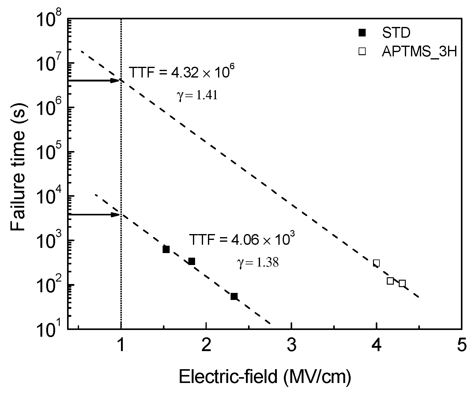
Figure 5 plots the measured media TTFs as a function of the applied electric-field for highly porous low-
k dielectrics without (full symbols) or with (open symbols) APTMS treatment for 3 h. Ten samples were measured for each condition. The measured TTFs decreased with the applied electric-field, indicating that the electric-field plays an important role in controlling the dielectric breakdown. Comparing with the measured TTFs of the pristine and APTMS-treated highly porous low-
k dielectrics, the latter sample had larger TTFs, indicating that the breakdown reliability of the highly porous low-
k dielectrics was enhanced by APTMS treatment due to the formation of SAMs. The pores in the dielectric film are considered to be defective sites and accelerate the dielectric breakdown [
22]. For the highly porous low-
k dielectrics with porosity larger than 30%, the neighboring pores are connected or interlinked to form opened-pores, causing more serious degradation in the dielectric breakdown. The SAMs on the highly porous low-
k dielectrics derived from APTMS treatment help to seal and isolate nanosized pores, retarding the formation of the connecting conductive path during a TDDB test. As shown in
Figure 5, the logarithm of the measured TTFs for both highly porous low-
k dielectrics without and with APTMS treatment displayed a linear relationship with the applied electric-field, implying that the breakdown mechanism can be described by the
E model. In the
E model, the breakdown mechanism is field-assisted bonding breaking and the expression is assumed to be TTF∼exp(-γE) [
23]. In this equation, γ is a field acceleration factor. The γ values were determined to be 1.38 and 1.41 for highly porous low-
k dielectrics without and with APTMS treatment. An increased γ value for APTMS-treated highly porous low-
k dielectrics helps further increase the dielectric failure time in a low operation field. In a field of 1.1 MV/cm, the failure time of APTMS-treated highly porous low-
k dielectric is calculated to be 1064 times larger than that of the pristine sample. This indicates a highly reliable dielectric breakdown for highly porous low-
k dielectrics is achieved by AMTMS treatment in aqueous phase in this study.
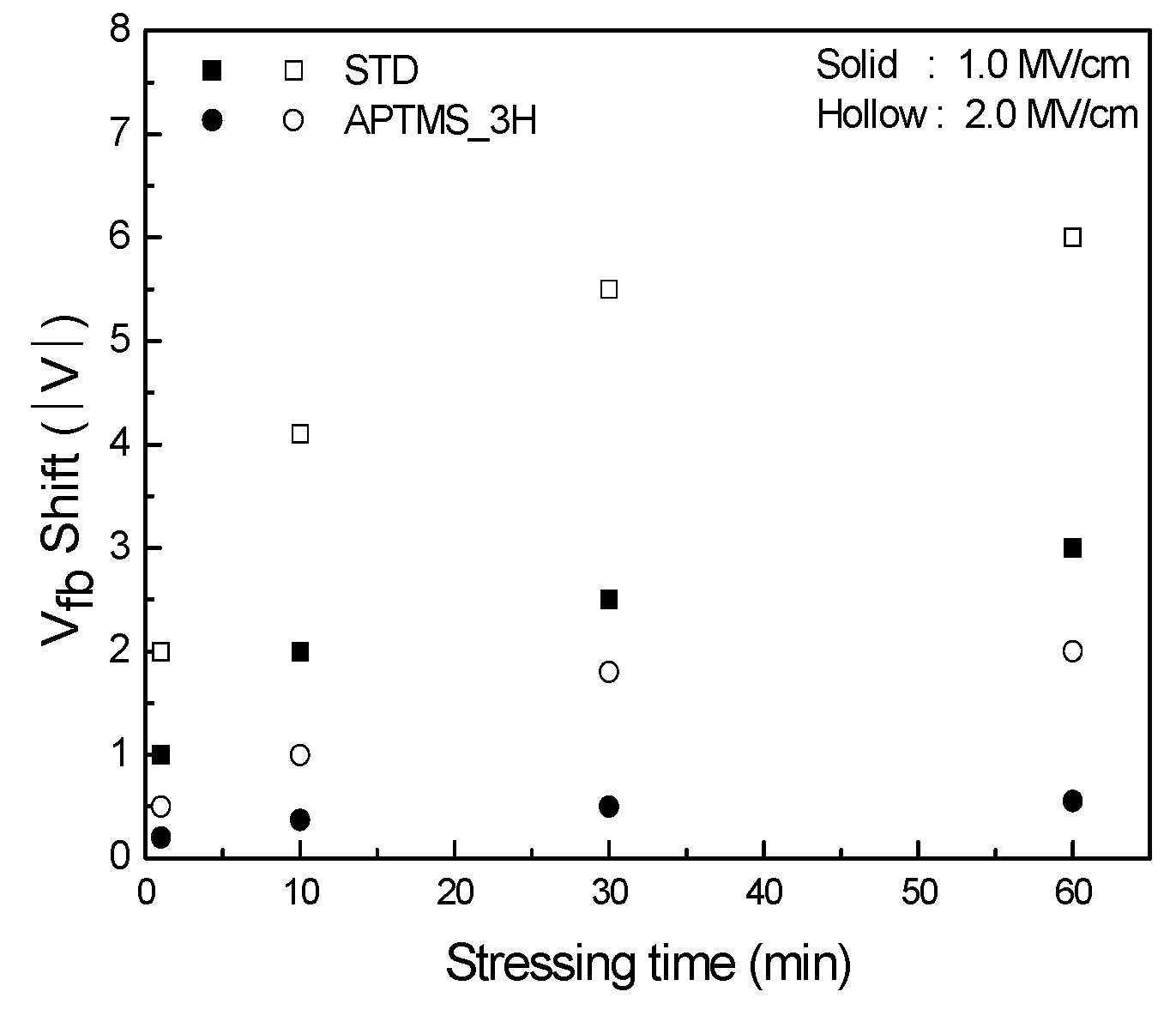
Cu easily penetrates into porous low-
k dielectrics under thermal or electrical stress. The drifted Cu ion can induce permanent bond displacement and catalyze the bond breakage reaction in the dielectric film, resulting in degraded electrical characteristics and reliability [
24,
25]. The formation SAMs on the highly porous low-
k dielectrics by APTMS treatment was stressed at different electric-fields at 25 °C for various times to evaluate its Cu barrier efficiency. After subjected to an electric stress at different intervals,
C–V characteristics were measured to determine the shift of flat-band voltage (
Vfb). For both highly porous low-
k dielectrics without and with APTMS treatment after electric stress, their flat-band voltage shifted toward negative voltage, representing the diffusion of Cu ions into the dielectric film [
26,
27].
Figure 6 compares the shift magnitude of flat-band voltage under an electric stress at 1.0 or 2.0 MV/cm as a function of stressing time for highly porous low-
k dielectrics without and with APTMS treatment. In cases of both highly porous low-
k dielectrics without and with APTMS treatment, an electric stress at a larger field yielded a larger flat-band voltage shift, indicating for faster Cu ion injection at a larger electric field. Moreover, the shift continuously increased toward negative voltage with stressing time, meaning for continuously Cu ions injection into the dielectrics with stressing time. The shift was strong after relatively short periods of stressing time and then saturated for a longer stressing time. The decreasing Cu ion concentration gradient is responsible for this feature. Compared with the results of the highly porous low-
k dielectrics without and with APTMS treatment, the APTMS-treated highly porous low-
k dielectric displayed a smaller flat-band voltage shift, indicating for less Cu ions injection into this material. Therefore, Cu barrier capacity of the highly porous low-
k dielectrics is strengthened by APTMS treatment. This also implies that the formation SAMs at the film’s surface by means of APTMS treatment has the function of blocking Cu ion diffusion.
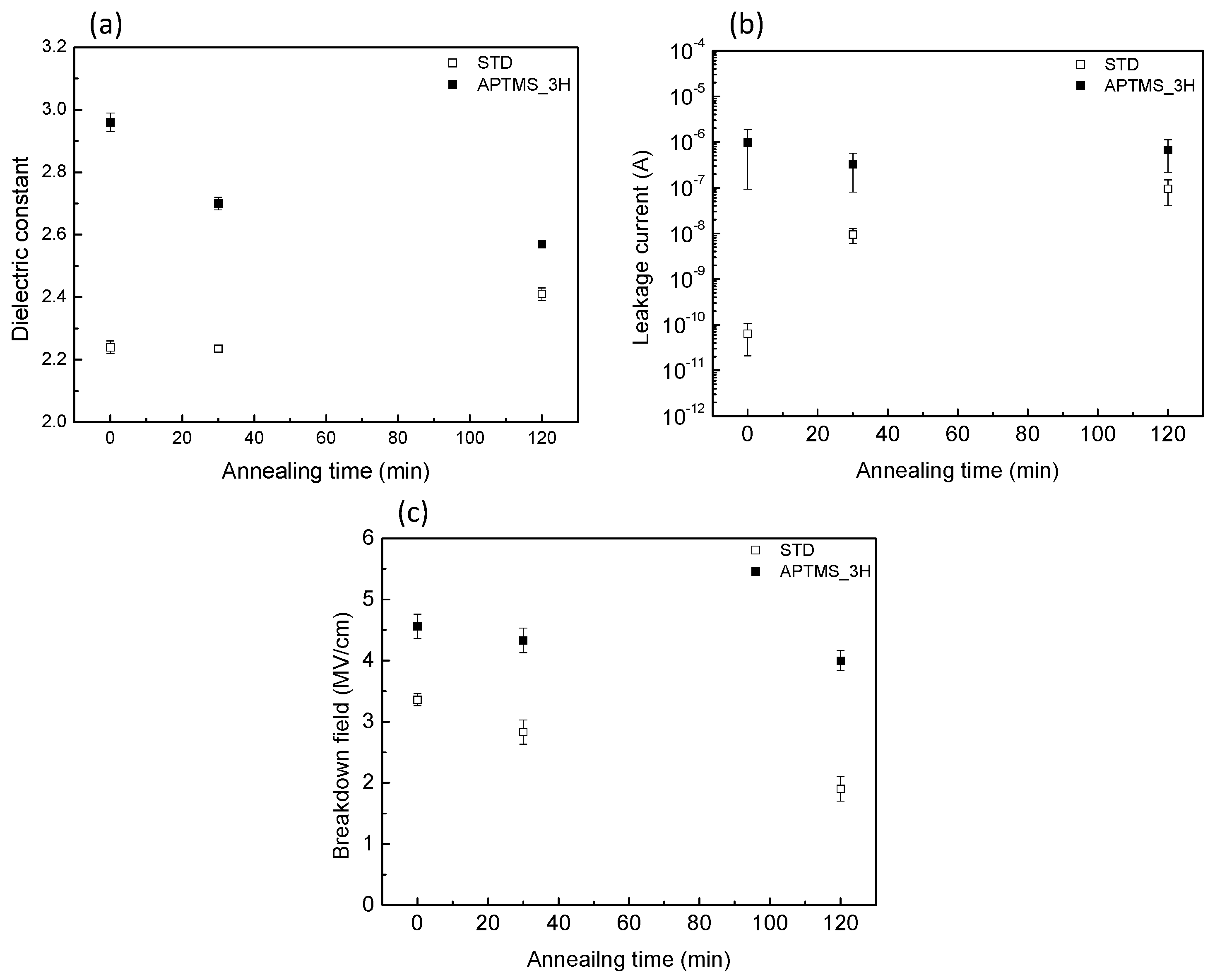
The thermal stability of APTMS-treated highly porous low-
k dielectrics was evaluated by a thermal stress at 450 °C for 30~120 min in an N
2 ambient. After annealing,
C–V and
I–V characteristics were measured.
Figure 7a–c plot the changes in the dielectric constant, leakage current at 2 MV/cm, and dielectric breakdown filed, respectively, with annealing time for highly porous low-
k dielectrics without and with APTMS treatment. For the pristine highly porous low-
k dielectrics without APTMS treatment, the measured electrical characteristics degraded with annealing time under an annealing at 450 °C. For the highly porous low-
k dielectrics with APTMS treatment, a reduced dielectric breakdown field was detected, although, the decreasing magnitude was not as large as that of the pristine sample. Thermal annealing easily drives Cu atoms to diffuse into the porous dielectric, thus degrading the dielectric breakdown field. A lower degradation in the highly porous low-
k dielectrics with APTMS treatment indicates again that the formation SAMs derived from APTMS treatment slowed down the thermal diffusion of Cu atoms. Bizarrely, for the highly porous low-
k dielectrics with APTMS treatment, the dielectric constant decreased and the leakage current at 2 MV/cm slightly decreased with annealing time under an annealing at 450 °C. Therefore, a thermal annealing on the APTMS-treated highly porous low-
k dielectric is required to optimize the electrical characteristics.
This study indicated that the formation SAMs by APTMS treatment improved Cu barrier ability and dielectric reliability for highly porous low-k dielectrics. The formation mechanism of SAMs derived from AMTMS treatment in aqueous solution was characterized by WCA, AFM, and XPS analyses. The water contact angle of the highly porous low-k dielectrics was 71°, then decreased to 17° after hydroxylation process, representing for the formation of hydrophilic Si–OH bonds at the film’s surface. By AMTMS treatment, the contact angle returned back to 69°. Therefore, the surface hydrophilic Si-OH bonds were replaced by hydrophobic groups from AMTMS. Moreover, the surface morphology of the highly porous low-k dielectrics was observed to be changed after APTMS treatment from AFM analysis, indicating that the film’s surface was modified (or SAMs formation). Additionally, the measured RMS values remained unchanged (~0.225 nm), implying that the formation SAMs at the surface of the highly porous low-k dielectrics is uniform.
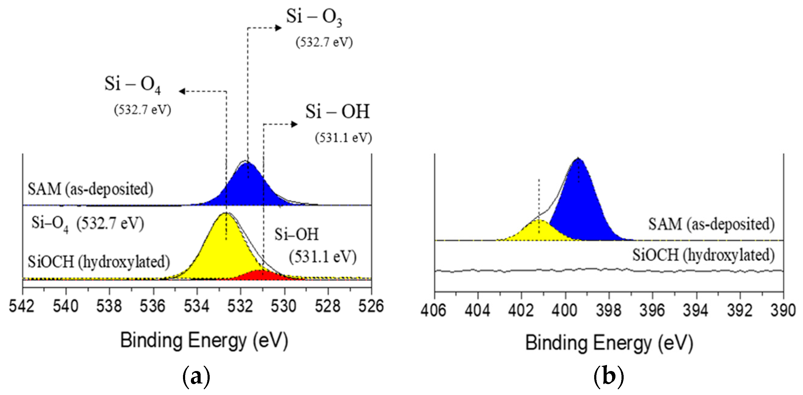
Figure 8a,b display O 1
s and N 1
s XPS spectrum, respectively, of the highly porous low-
k dielectrics after hydroxylation and APTMS treatment. The hydroxylated sample exhibited an O 1
s main peak at a binding energy of 532.7 eV from bulk oxygen atoms (Si–O–Si, i.e., Si–O
4) [
27,
28], along with a minor peak centered at 531.1 eV from surface silanol (Si–OH) groups [
28]. After APTMS treatment, the peak of Si–OH groups obviously decreased, indicating that the transformed Si–OH groups were replaced. Moreover, the binding energy of Si–O–Si group shifted to 531.7 eV, corresponding to Si–O
3 linkages [
29]. For N 1
s signal, no any peak was observed in the highly porous low-
k dielectrics before and after hydroxylation. However, N 1
s spectra appeared in the APTMS-treated highly porous low-
k dielectric, confirming the formation of a highly oriented SAMs from APTMS. Deconvoluting N 1
s peak can result in two peaks at binding energies of 399.3 eV and 401.2 eV, attributed to primary (–NH
2) and protonated (–NH
3+) amino groups, respectively [
30,
31]. Moreover, the higher the percentage of –NH
2 groups (~82%) implies that the formation SAMs are highly oriented [
31]. These N-related groups in the SAMs are benefit for Cu barrier [
32].
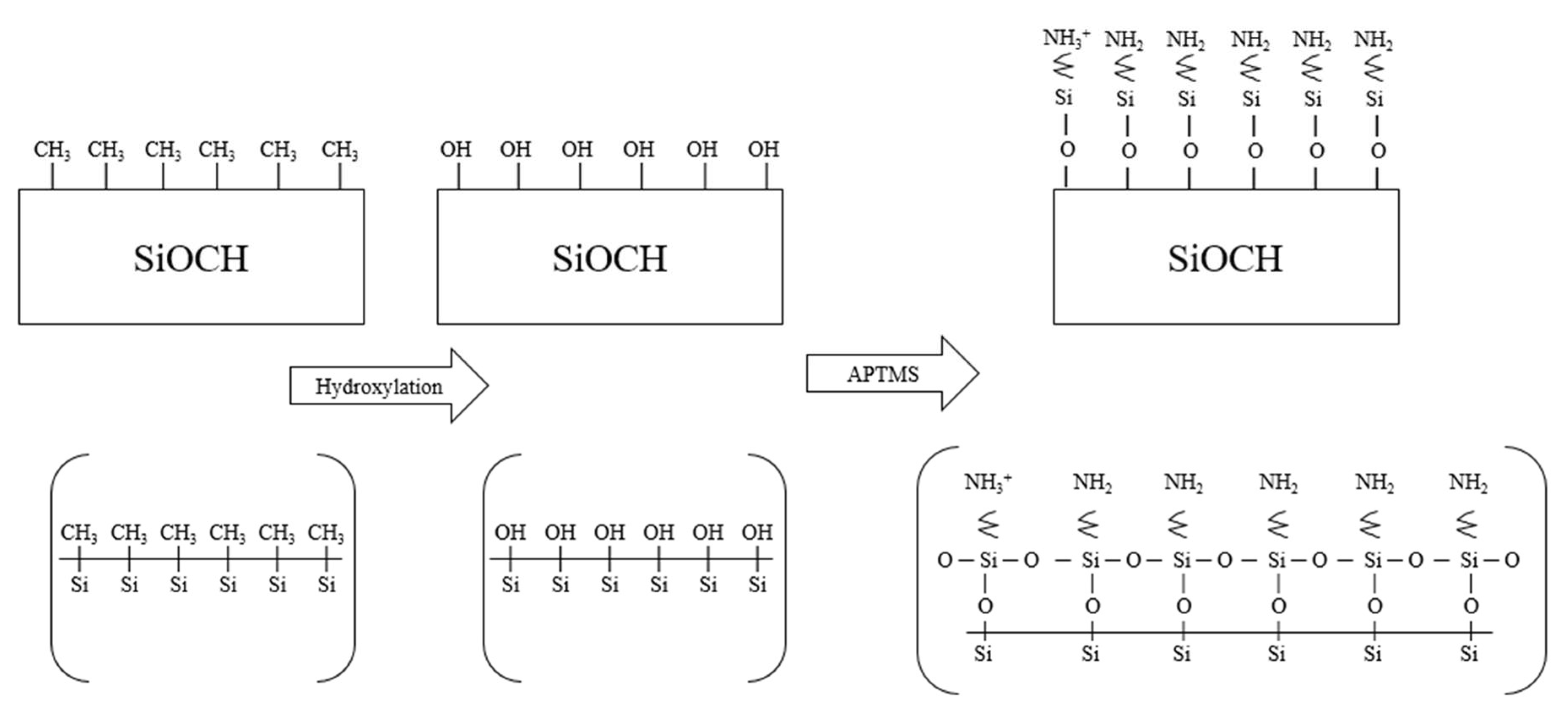
According to the above analyses, the formation mechanism of SAMs derived by APTMS treatment in aqueous phase on the highly porous low-
k dielectric (i.e., SiOCH film) can be expressed in the following schematic, as shown in
Figure 9. First, in the hydration step, Si–CH
3 bondings at the surface of SiOCH film were converted to Si–OH (silanol) groups by salinization reaction. Next, in the APTMS aqueous solution, AMTMS organic agents react with silanol groups on the salinized highly porous low-
k surface, forming –O–Si–(CH
2)
3–NH
2 end groups at the film surface. In the solution, some –NH
2 groups accept H
+ to form –NH
3+ conjugated groups.
