1. Introduction
Tungsten oxide (WO
3), as a wide bandgap semiconductor, has been intensively investigated for various uses in scientific devices [
1,
2]. Among various applications, the photocatalyst application for degrading organic pollutants receives much attention as WO
3 has the advantages of low cost, high chemical stability, and excellent process-dependent reproducibility. In general, pure WO
3 crystal shows five phase transitions at temperatures ranging from −180 to 900 °C [
3]. Among the five crystal forms, a monoclinic I WO
3 phase is the stable phase at room temperature. However, the orthorhombic WO
3 phase exists only in some WO
3 nanostructures at room temperature, not frequently visible for other morphologies such as a thin-film structure. This is attributable to the fact that the transition temperature of the orthorhombic WO
3 phase for WO
3 nanostructures is generally at room temperature, which is quite lower than that of bulk WO
3.
WO
3 in a thin-film structure is highly desirable for various device applications because thin solid film can be integrated into various small devices or combined with other materials to form composites for scientific applications. Several methods of manufacturing WO
3 thin films with various microstructures for applications have been reported. For example, the pulsed-laser deposited WO
3 thin films are integrated with TiO
2 thin films to form multilayer films and used for photodegradation of methylene blue (MB) solution. The WO
3 layer in the multilayer structure enhances the photocatalytic ability of the TiO
2 layer [
4]. The spray pyrolysis synthesized WO
3 thin films have also been used for photodegrading methyl orange (MO) [
5]. The thermal evaporation deposited WO
3 thin films with adequate postannealing procedures in an oxygen-rich environment at 500 °C for 1 h have been used to degrade MB under irradiation [
6]. Radio-frequency (RF) sputtering deposited WO
3/TiO
2 bilayer thin films with various WO
3 content are used to enhance the photocatalytic activity of TiO
2-based materials [
7]. However, most WO
3 thin films synthesized through various methods are in a monoclinic structure; that is, the orthorhombic structure is limited in number.
Among various physical synthesis methods for WO
3 thin films, sputtering has been widely used to prepare oxide thin films with controllable microstructures and tunable physical properties. Moreover, the DC sputtering deposited WO
3 thin films via a metallic tungsten target provide the advantages of low cost and highly recycled usage of the target in comparison with those in WO
3 ceramic targeted by radio-frequency sputtering. Although DC sputtering growth of monoclinic or amorphous WO
3 thin films have been investigated for applications in gas-sensing, photocatalytic, and electrochromic devices, reports on the microstructure-dependent photodegradation properties of DC sputtering deposited orthorhombic WO
3 photocatalysts toward organic dyes are still lacking. Karuppasamy et al. synthesized amorphous WO
3 thin films via DC sputtering under various oxygen pressures. This work revealed that WO
3 films deposited at a lower working pressure exhibit satisfactory electrochromic properties. The variation of bulk density of the films prepared at various oxygen pressures affects the efficiency of insertion and removal of protons and electrons [
8]. Kim et al. used DC sputtering to deposit monoclinic WO
3 films with various degrees of crystallinity by controlling the growth temperature from 200–500 °C. Higher crystal quality of WO
3 films deposited at a higher temperature resulted in better gas-sensing ability [
9]. WO
3 films consisting of nanostructured surface feature are prepared by DC sputtering at various working pressures. The as-synthesized monoclinic WO
3 thin films are further used to photodegrade stearic acid [
10]. Moreover, Stolze et al. prepared amorphous WO
3 films via DC sputtering under various O
2 percentages ranging from 0 to 20 vol.%; the effects of stoichiometry of WO
3 films on electrochromic properties were discussed [
11]. The aforementioned examples demonstrate that most work on DC sputtering WO
3 films mainly focused on the monoclinic or amorphous phase. Reports on in-situ DC sputtering growth of orthorhombic WO
3 thin films are limited in number; this is associated with the fact that the orthorhombic structured WO
3 is unstable when the substrate temperature of the sputtering process is cooled down to room temperature. Therefore, the strategy to resolve this issue is to grow amorphous WO
3 films under a low oxygen content atmosphere, and then conduct various annealing procedures to obtain the stable orthorhombic WO
3 phase. Furthermore, the microstructure-dependent photocatalytic properties of the orthorhombic WO
3 films are presented in this study. The results herein might be useful for designing orthorhombic WO
3 thin-film photocatalysts with a desirable photodegradation ability toward organic dyes.
3. Result and Discussions
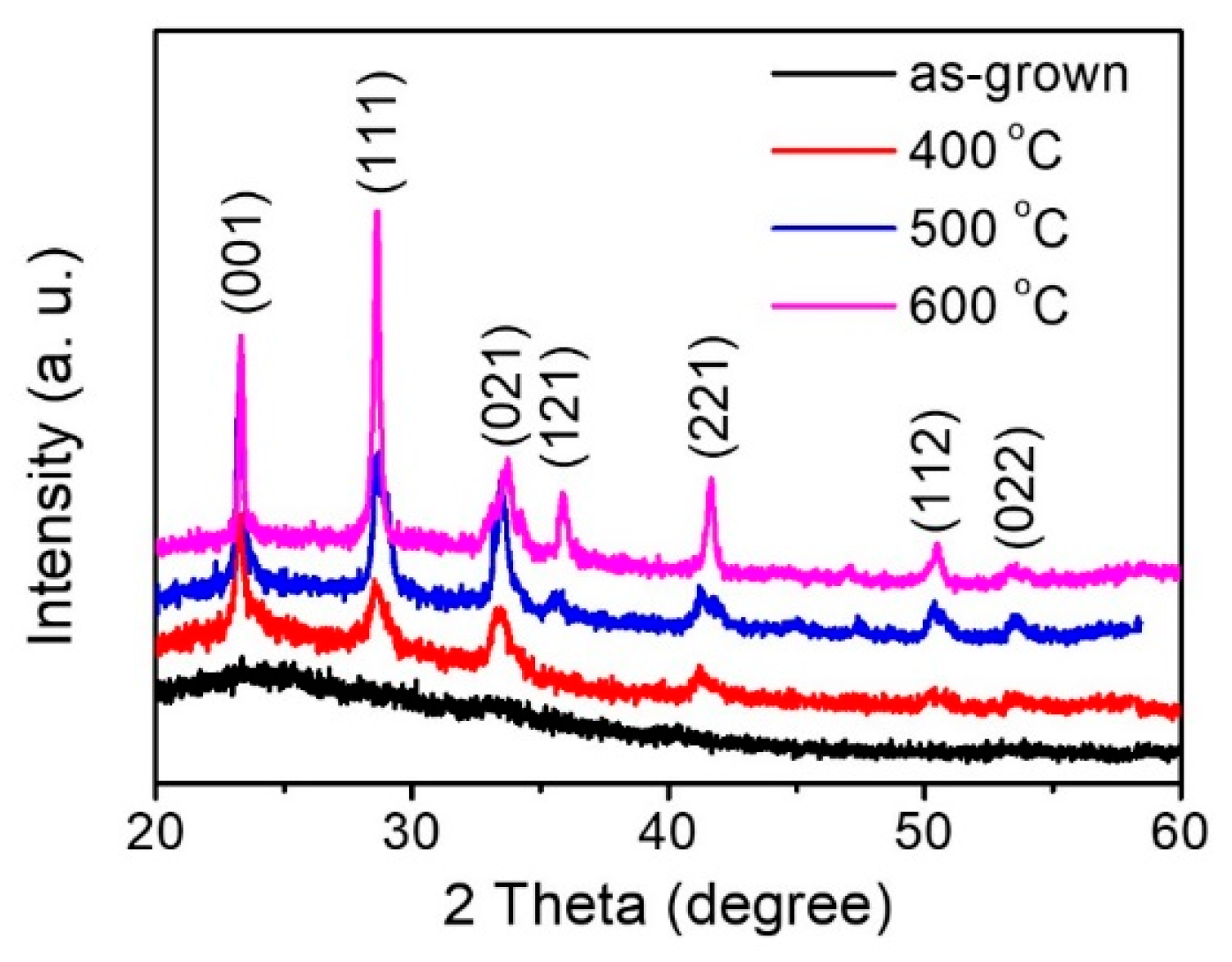
The change in crystal structure features of the WO
3 thin films with various thermal annealing procedures is depicted in
Figure 1. The as-grown WO
3 film shows an amorphous structure, as no visible Bragg reflections are found.
Figure 1 shows the XRD patterns of the WO
3 films with thermal annealing procedures at 400–600 °C. The orthorhombic crystalline WO
3 phase is formed with distinguishable Bragg reflections (JCDPS. 20-1324). The more intense Bragg reflections associated with a narrower full-width at half maximum were observed for the thin films annealed at a higher annealing temperature, revealing a higher degree of crystalline quality of the film. Notably, no other peaks of impurities were observed after thermal annealing procedures. The XRD results reveal that the as-grown WO
3 thin films exhibited a polycrystalline feature after postannealing. The crystallite sizes of the annealed WO
3 films were evaluated using the Scherrer formula [
12]. The crystallite sizes of the WO
3 films annealed at 400, 500, and 600 °C were approximately 24, 32, and 57 nm, respectively. The (001)-oriented crystal dominated the crystal structure feature of the crystalline WO
3 thin films annealed below 500 °C; moreover, the (111)-oriented crystal dominated the crystal structure feature when the film was annealed at 600 °C. Notably, the change of the WO
3 crystal orientation from (001) to (111) at the higher temperature annealing is associated with the surface binding energy among the low index crystallographic planes [
13].
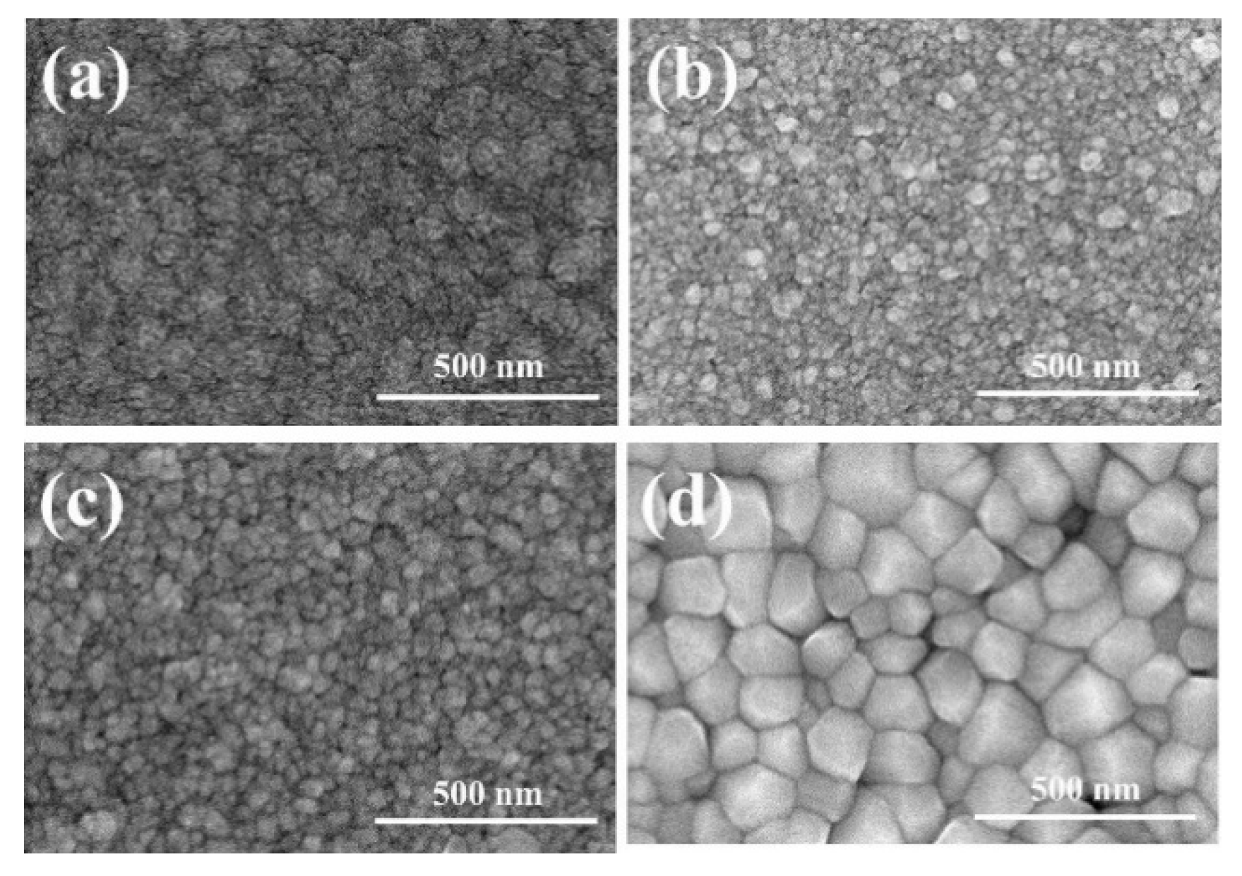
Surface morphologies of the WO
3 thin films with and without thermal annealing are shown in
Figure 2. No distinctly well surface grain features can be seen for the as-grown WO
3 (
Figure 2a). This might be associated with the amorphous nature of the sample as characterized by the XRD measurement. When the film was annealed at 400 °C, a surface grain feature was visible and the surface grains had an average size of approximately 32 nm (
Figure 2b). Further increasing the annealing temperature to 500 °C increased the size of surface grains, and the homogeneity of grain size improved simultaneously. The average surface grain size was approximately 51 nm evaluated from
Figure 2c. Notably, the surface grain size was abnormally increased (average grain size of 102 nm) and an uniformly cylindrical crystal feature was obtained when the film was annealed at 600 °C (
Figure 2d). The high annealing temperature provides sufficient energy, which might facilitate the coalescence of the adjacent tiny crystals, and therefore large surface grains were formed.
Furthermore, the surface roughness of the various WO
3 thin films was further characterized by AFM.
Figure 3a exhibits the surface of the as-grown WO
3 thin film. The root mean square (RMS) roughness of the as-grown amorphous WO
3 thin film was evaluated to be approximately 3.55 nm. Comparatively, the WO
3 thin films annealed at 400–600 °C exhibited coarser surface morphology (
Figure 3b–d). The RMS roughness values of the WO
3 thin films were of approximately 4.02, 4.75, and 9.28 nm corresponding to the annealing temperature of 400, 500, and 600 °C, respectively. This result demonstrated that the surface roughness monotonically increases with increasing annealing temperature because high annealing temperature facilitates the coalescence of the surface grains and therefore rougher surface. The average surface grain sizes of the WO
3 thin films annealed at 400, 500, and 600 °C were approximately 26, 43, and 84 nm, respectively. Larger surface grains of the annealed film engendered a rougher surface feature. Similarly, a substantially increased surface grain size, as reported in the CuO film, annealed at the temperature higher than 700 °C [
14].
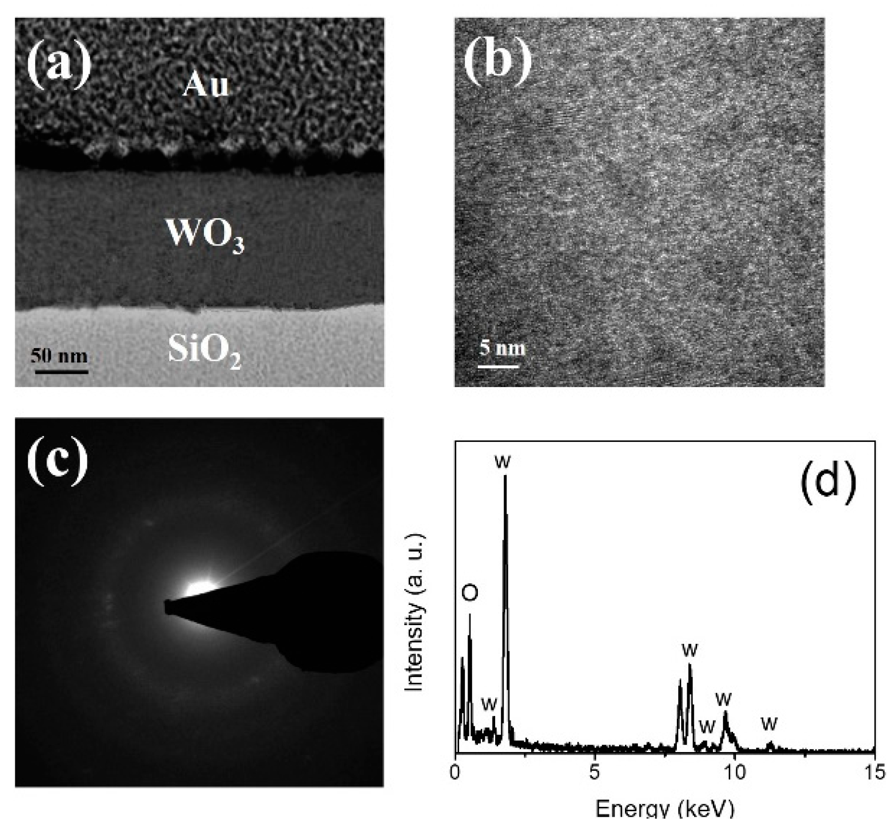
The detailed microstructures of the WO
3 thin films with and without thermal annealing at 600 °C were investigated by TEM. A low-magnification, cross-sectional TEM image of the as-grown WO
3 thin film is shown in
Figure 4a. The thickness of the WO
3 film was ~120 nm. The film surface is dense and smooth, and no voids can be seen. A high-resolution TEM (HRTEM) micrograph of the as-grown WO
3 thin film is depicted in
Figure 4b. The random and chaotic lattice fringes with a short-range order are distributed over the area of interest, revealing that the film is in the amorphous phase. Moreover, the selected area electron diffraction (SAED) pattern in
Figure 4c exhibits a faint ring-like pattern, revealing that the film without heat treatment is uncrystallized. This is in agreement with the XRD result.
Figure 4d depicts the energy-dispersive X-ray spectroscopy (EDS) spectra of the film, confirming that the film’s composition consisted of W and O. Moreover, the O/W composition ratio is approximately 2.48, demonstrating oxygen deficiency in the WO
3 thin film. This is often observed in oxide thin films prepared by sputtering because the thin film growth condition is in an oxygen deficient environment during sputtering [
15].
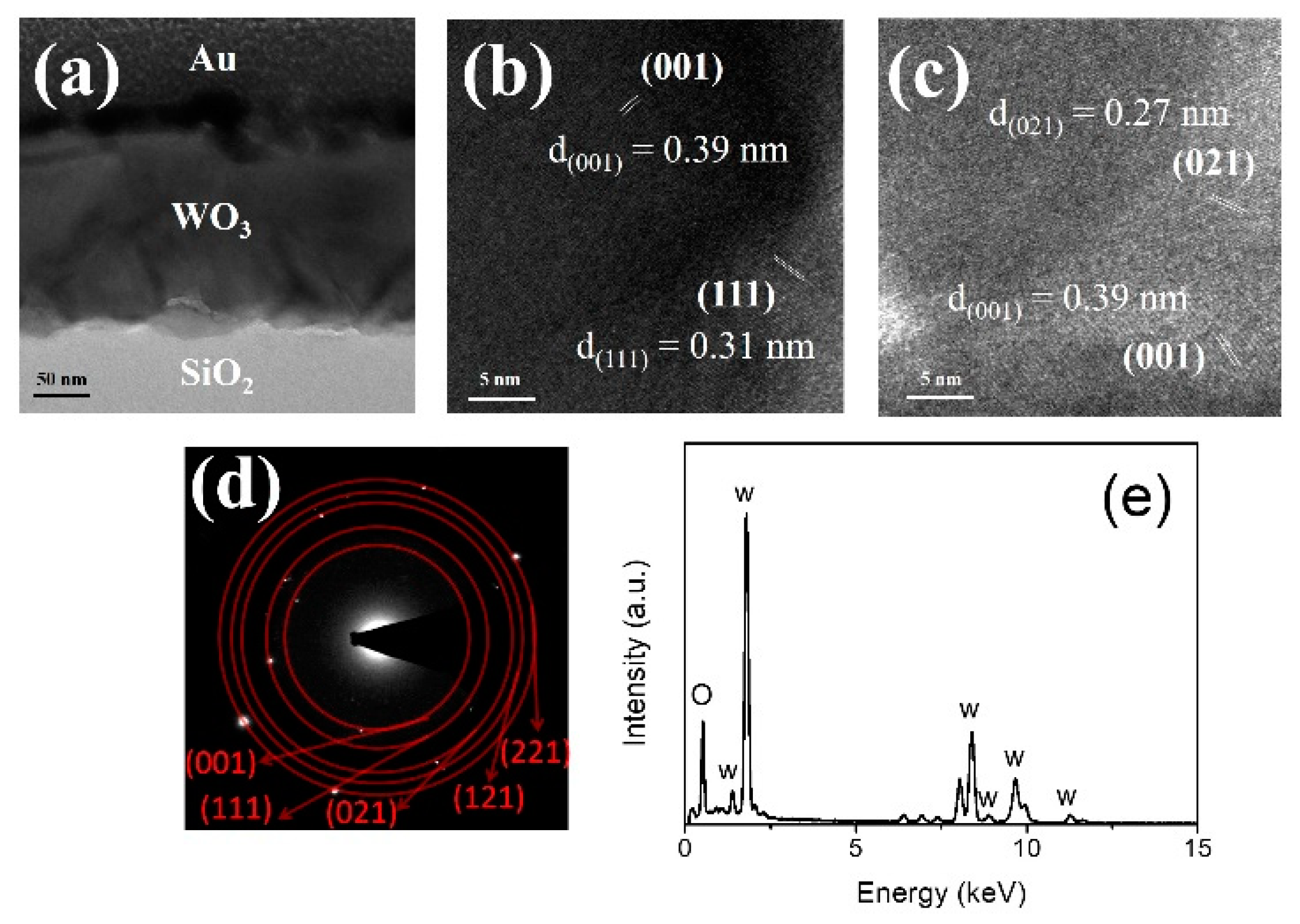
Figure 5a depicts a low-magnification, cross-sectional image of the WO
3 film annealed at 600 °C. The film thickness of the annealed WO
3 film is homogeneous throughout its cross section. Compared to the as-grown film, the surface and root of the high-temperature-annealed film are more undulated.
Figure 5b,c demonstrate HRTEM images of the annealed WO
3 thin film. The appearance of visible and ordered lattice fringes in the HREM images indicate that the WO
3 film after annealing had a high degree of crystallinity. The atomic lattice fringes with intervals of approximately 0.39, 0.31, and 0.27 nm could be identified and were attributed to the interplanar distances of the WO
3 (001), (111), and (021) crystallographic planes, respectively. The boundaries between the adjacent grains were visible. The polycrystalline nature and the orthorhombic structure of the WO
3 film were also confirmed by the SAED measurements in
Figure 5d. Distinct diffraction spots arranged in centric rings revealed the crystalline WO
3 thin film was formed after the 600 °C annealing process.
Figure 5e shows the EDS spectra; the spectra revealed that the film mainly composed of W and O. No other impurity atoms were detected.
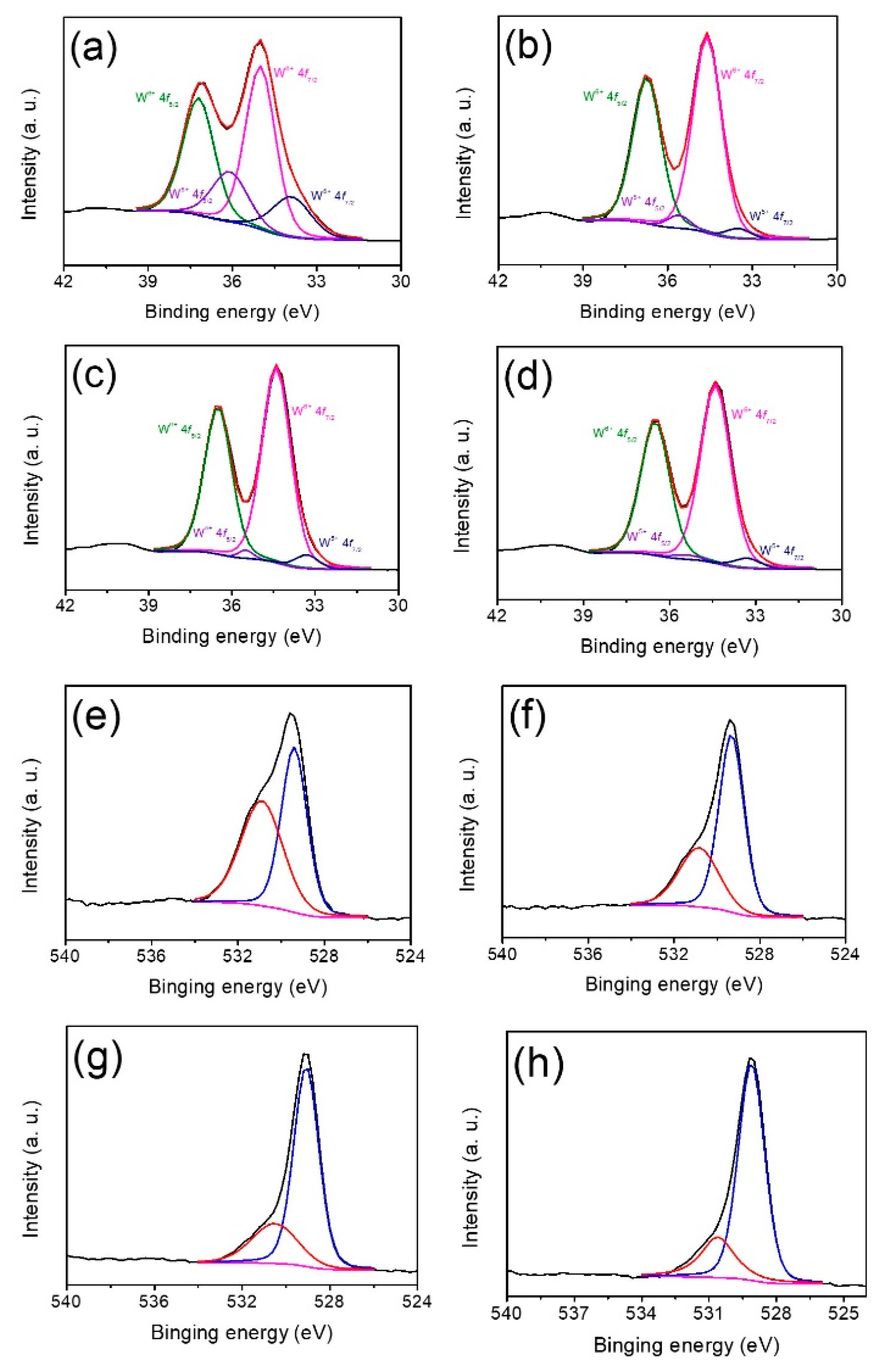
XPS analysis was performed to reveal the elemental binding states of various WO
3 thin films. The annealing temperature-dependent W oxidation state change is shown in
Figure 6a–d. From the figures, the intense doublet with binding energies of approximately 35.0 eV (W4
f7/2) and 37.2 eV (W4
f5/2) are associated with photoelectrons emitted from W
6+ ions of the WO
3 films, while the relatively small peaks at 34.0 and 36.2 eV can be assigned to W4
f7/2 and W4
f5/2 of W
5+ oxidation state in tungsten oxides [
16]. The presence of W
5+ suggests the existence of crystal defects in the WO
3 film. Comparatively, the area and the height of core level W
5+ decreased after annealing, which implied increased oxidation states of W in the WO
3 film. Notably, the WO
3 film annealed at 600 °C had the smallest features of W
5+, which indicates the surface tungsten in this film exhibited a larger degree of oxidation state after annealing. No peaks attributed to metallic W were identified in the spectra of all films. Notably, the W/O atomic ratio of the as-grown WO
3 film was approximately 0.4. Moreover, the W/O atomic ratio of the WO
3 films decreased from 0.37 to 0.34 with the annealing temperature increasing from 400 to 600 °C, respectively, evaluated from the XPS analyses.
Figure 6e–h show that the XPS spectra of O1
s for various WO
3 thin films have an asymmetric curve feature. The O1
s spectra of the surface of various WO
3 thin films were fitted by two distributions, centered at approximately 529.3 and 530.8 eV, respectively. The relatively low binding energy peak is attributed to O
2− ions in the oxide lattice. The higher binding energy peak is attributed to the oxygen vacancies in the WO
3 [
17]. The relative content of the oxygen vacancy for various WO
3 films was evaluated according to the area ratio of these two deconvolution components: (red peak)/(red peak + blue peak). The relative area of the higher energy binding component for the WO
3 films decreased with the annealing temperature. A great amount of vacancy existed in the surface of the as-grown WO
3 film. After annealing, the surface oxygen vacancy content markedly decreased from 34.4% to 25.3% with the annealing temperature increasing from 400 to 600 °C, respectively.
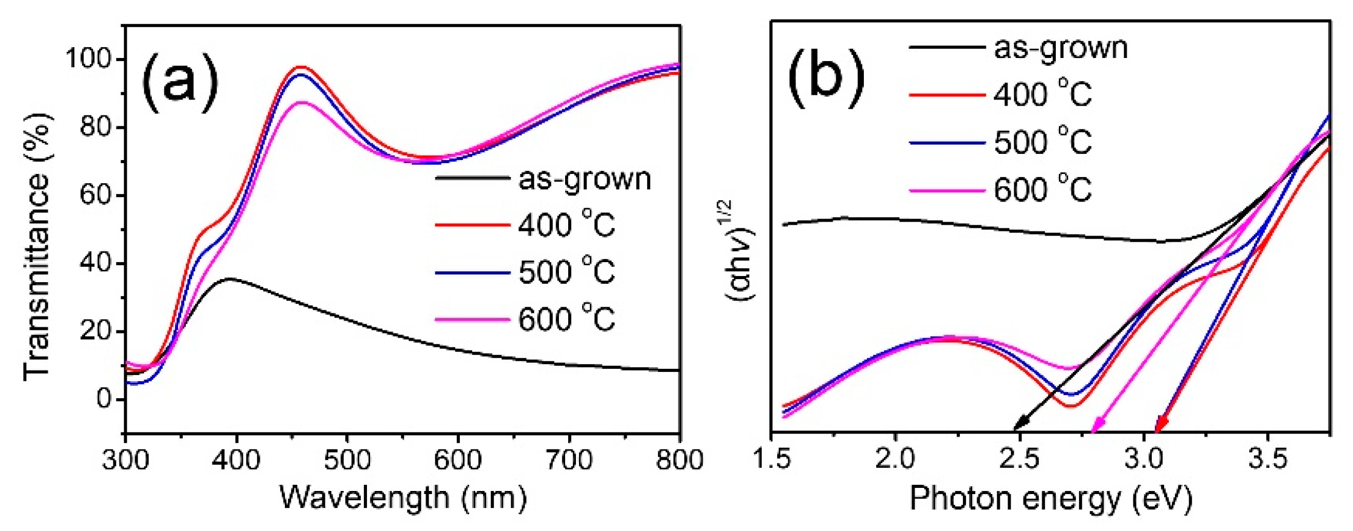
The transmittance spectra of the WO
3 thin films with and without annealing are demonstrated in
Figure 7a. The light was highly absorbed in the visible region with less than 40% transmittance for the as-grown WO
3 film, attributed to the presence of massive oxygen-related defects. Moreover, the as-grown WO
3 film is seen in semi-transparent bluish color, which shows the amorphous and highly non-stoichiometric natures of the film [
18]. The highly transparent feature was observed for the WO
3 films conducted with annealing; moreover, no blue colouration appeared in the samples. The enhancement in the transmittance degree of the annealed WO
3 films is due to the reduction of oxygen-related crystal defects, which might play an important role in scattering the incident light. Notably, a clear shoulder feature appeared at approximately 350 nm for the films annealed below 600 °C. That shoulder feature in the optical transmittance spectra is associated with the residual crystal defects associated with oxygen deficiencies in the samples [
19]. Notably, the shoulder feature completely vanished for the WO
3 film conducted with thermal annealing at 600 °C, indicating that the oxygen-related crystal defects of the film were substantially removed in the annealing process. The bandgap value of various thin-film samples is calculated by plotting (α
hv)
1/2 vs. photon energy using the following formula:
where α is the absorption coefficient, A is a constant,
hv is the energy of an incident photon,
Eg is the bandgap value. On extrapolating the linear portion of the curves (
Figure 7b), the intercept on the energy axis (α
hv)
1/2 = 0 gives the value of the indirect bandgap energy. The bandgap values were calculated as 2.48, 3.04, 3.04, and 2.78 eV for as-grown and annealed WO
3 samples at 400, 500, and 600 °C, respectively. The as-prepared WO
3 thin film exhibited the smallest bandgap value and may be associated with a relatively large content of oxygen deficiencies in the film as compared to the annealed ones. Due to the existence of a high density of oxygen-deficient crystal defects, they might form new discrete energy bands below the conduction band, resulting in the relatively low band gap. After annealing at 400 and 500 °C, the
Eg of two WO
3 thin-film samples originates from the recombination of free carriers from the bottom of the conduction band energy to the valence band energy with the decreased discrete energy bands after thermal annealing. It was noticed that the bandgap value of the WO
3 film further decreased at the highest annealing temperature of 600 °C, assigned to explosive growth in grain size of the WO
3 film [
20].
Figure 8a–d show the absorbance spectra of the MB solution in the presence of various WO
3 thin films at different irradiation times. After the MB solution was illuminated, the absorbance peak intensity at ~663 nm was observed to gradually decrease with duration, implying that MB molecules are photodegraded. The photodegradation degrees (
C/
C0) of the MB solution containing various WO
3 thin films are summarized in
Figure 7e. The
C0 is concentration MB solution without irradiation and
C is the residual concentration of the MB solution after irradiation at a given duration. Notably, the
C/
C0 values of the MB solution containing various WO
3 thin films under various dark conditions are demonstrated in
Figure 7e. A slightly decrease of
C/
C0 value was observed for the dark balance of 120 min; this is attributed to the fact that partial MB molecules were absorbed on the surface of the WO
3 thin films under dark balance condition. By contrast, the photodegradation rates of the MB solution with various WO
3 thin films are different. As demonstrated in
Figure 8e, the WO
3 film conducted with thermal annealing at 600 °C was most catalytically efficient, giving a photodegradation extent of approximately 45% in 30 min, while other annealed thin films photodegraded only 35% of MB in the same time period. After 120 min irradiation, the WO
3 film annealed at 600 °C still displayed the largest degree of photodegradation toward the MB solution. Notably, under irradiation, WO
3 was photoexcited and the e
−/h
+ pairs were formed. The e
− can participate in organic pollutant degradation reactions. The possible formations of the superoxide anion, hydroperoxyl, and hydrogen peroxide (H
2O
2) species in the organic dye solution are advantageous for further degrading the MB dyes [
21]. However, it has been shown that the position of the conduction band of WO
3 (+0.50 V vs. NHE) was below the standard redox potential for the formation of superoxide anion (−0.33 V vs. NHE) and hydroperoxyl (−0.046 V vs. NHE) [
22]. Based on the aforementioned, the following reactions are therefore more likely to occur during the MB photodegradation process using WO
3 thin films as photocatalysts:
Meanwhile, the photogenerated h
+ in the WO
3 might involve the reactions and form •OH radicals through the following equations:
The produced •OH radicals are efficiently degrading species for the MB dyes. Although the band position of the WO3 is advantageous for the photodegradation mechanism, the microstructure and optical properties should be considered for the final photodegradation efficiency. The WO3 film with thermal annealing performed at 600 °C was the most active photocatalyst, and the films annealed at lower temperatures were somewhat less active in this work. In contrast, the as-grown WO3 film had a lower photocatalytic activity. We assume that the deteriorated crystal quality of the WO3 with the lower annealing temperatures or without annealing was the decisive factor in their inferior photodegradation activity. Fewer oxygen-deficient-related defects in the lattice of the WO3 film annealed at 600 °C might result in fewer recombination centers in the film, which would be detrimental for the higher photodegradation efficiency in this study. Moreover, the relative lower optical bandgap value of the WO3 film conducted with thermal annealing at 600 °C among different annealed thin films is another advantageous factor to increase the light harvesting and enhance the degradation ability of crystalline WO3 film toward MB dyes under irradiation.


