Transparent p-Type Semiconductors: Copper-Based Oxides and Oxychalcogenides


Abstract
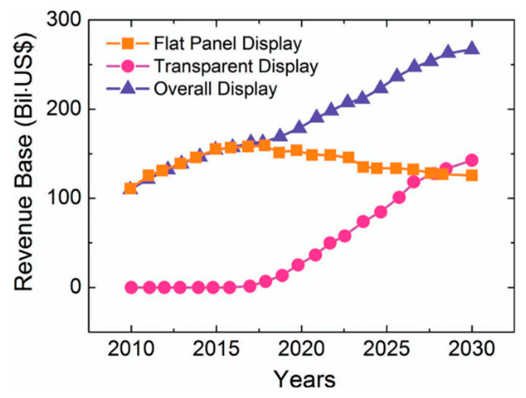
1. Introduction
2. Preparation and Properties of Materials
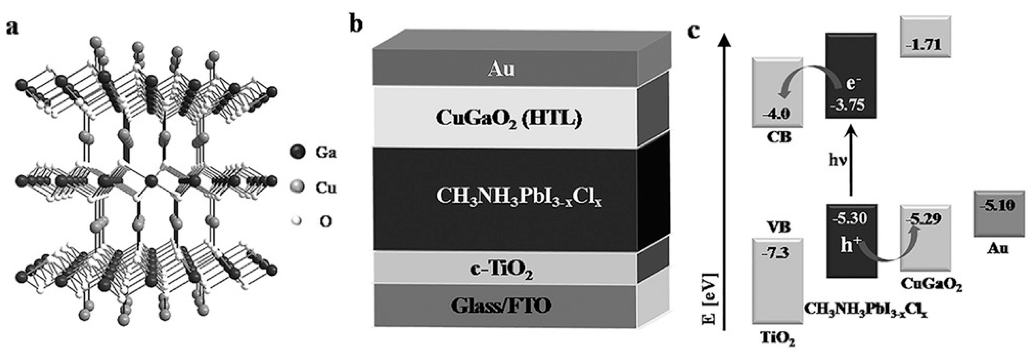
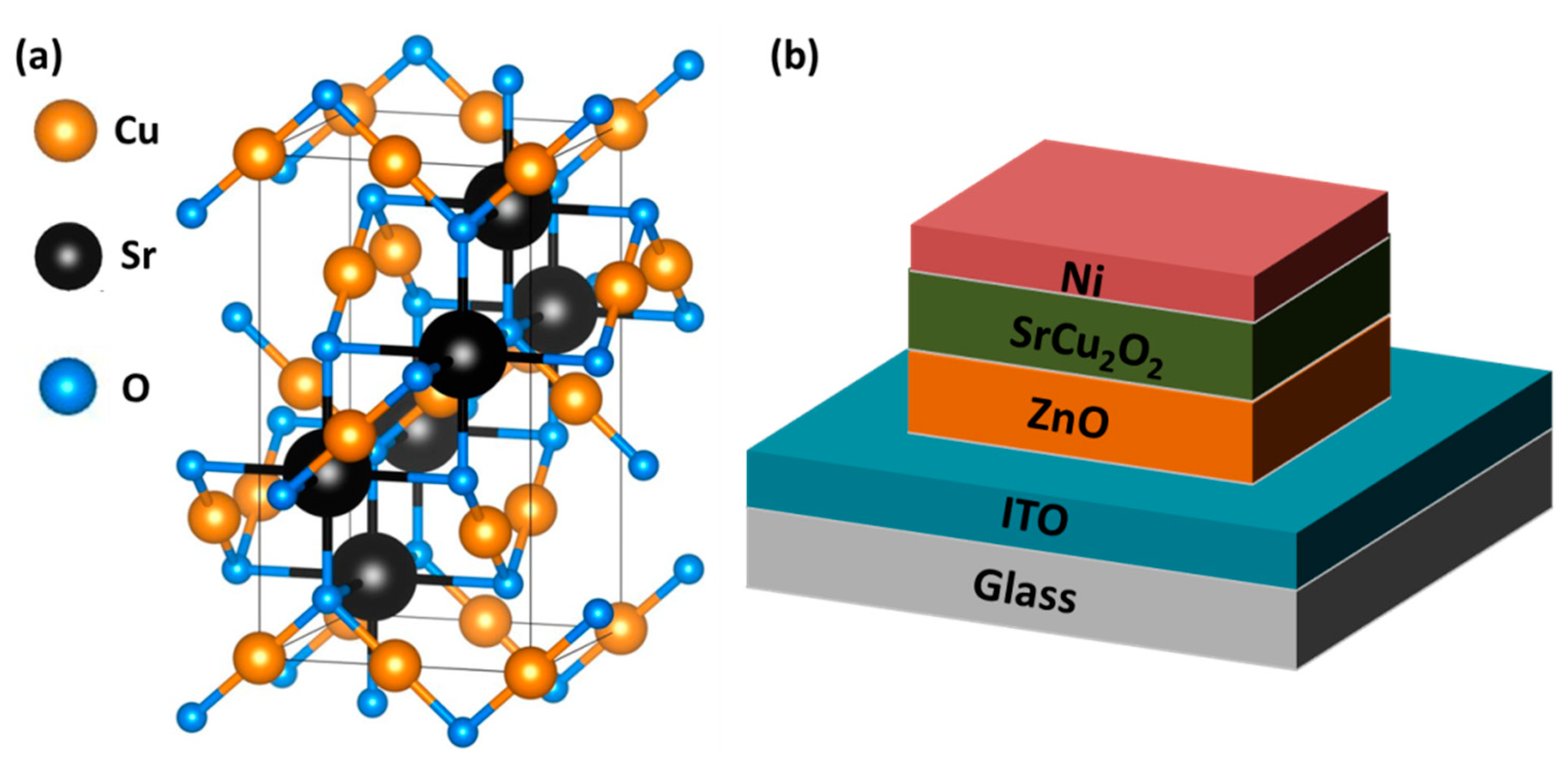
2.1. Delafossite (CuMO2)
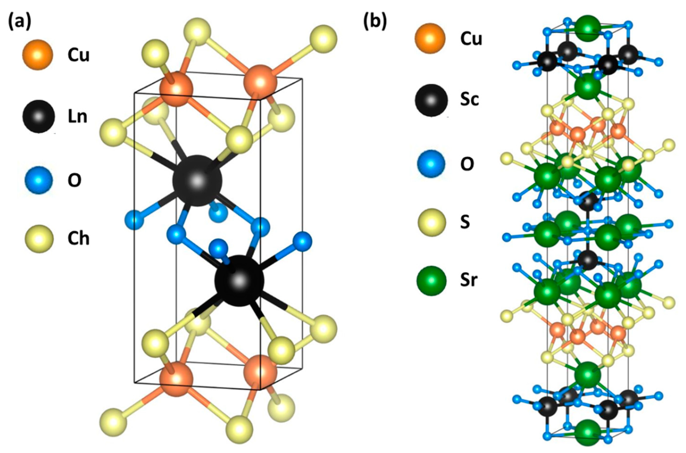
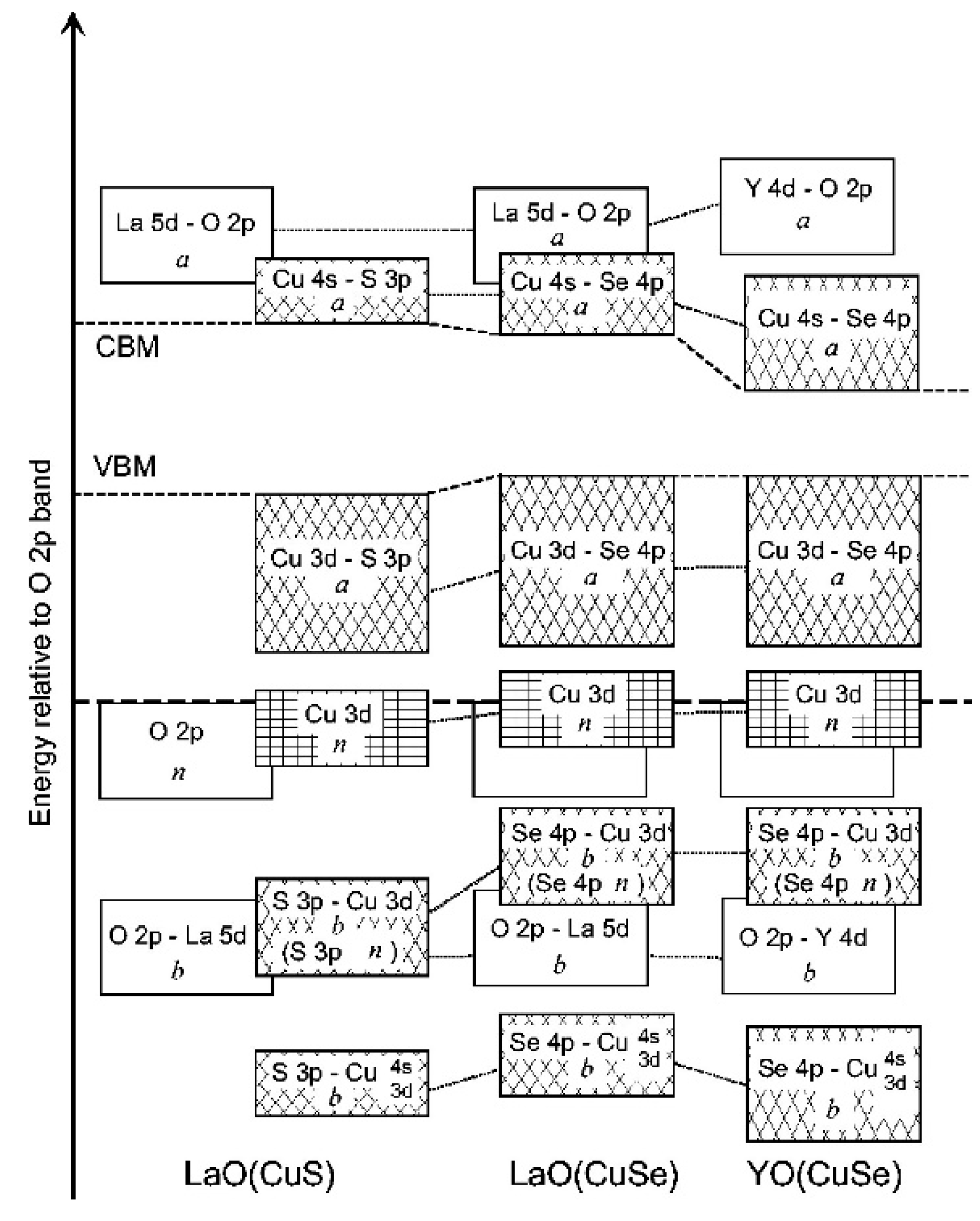
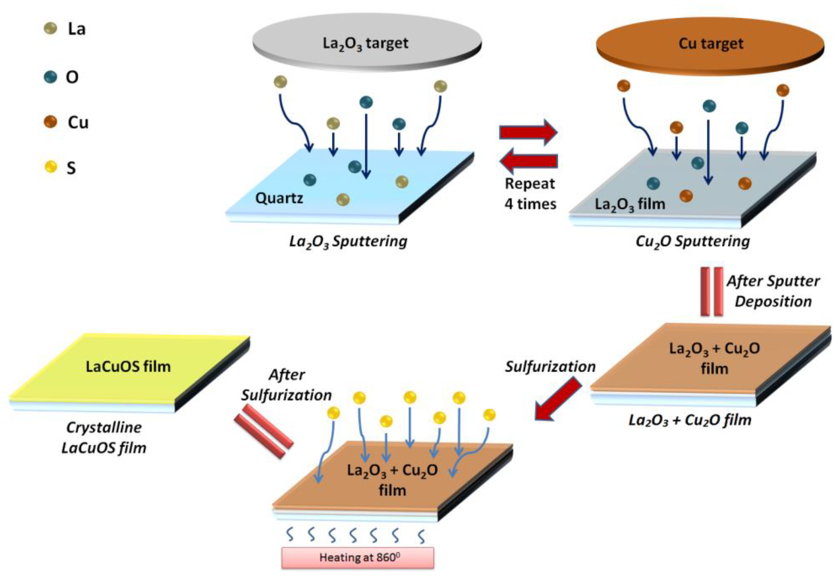
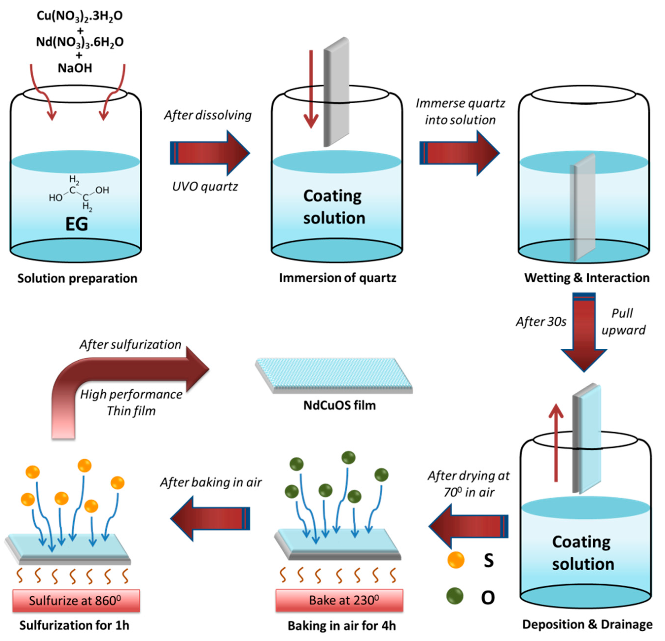
2.2. Oxychalcogenides
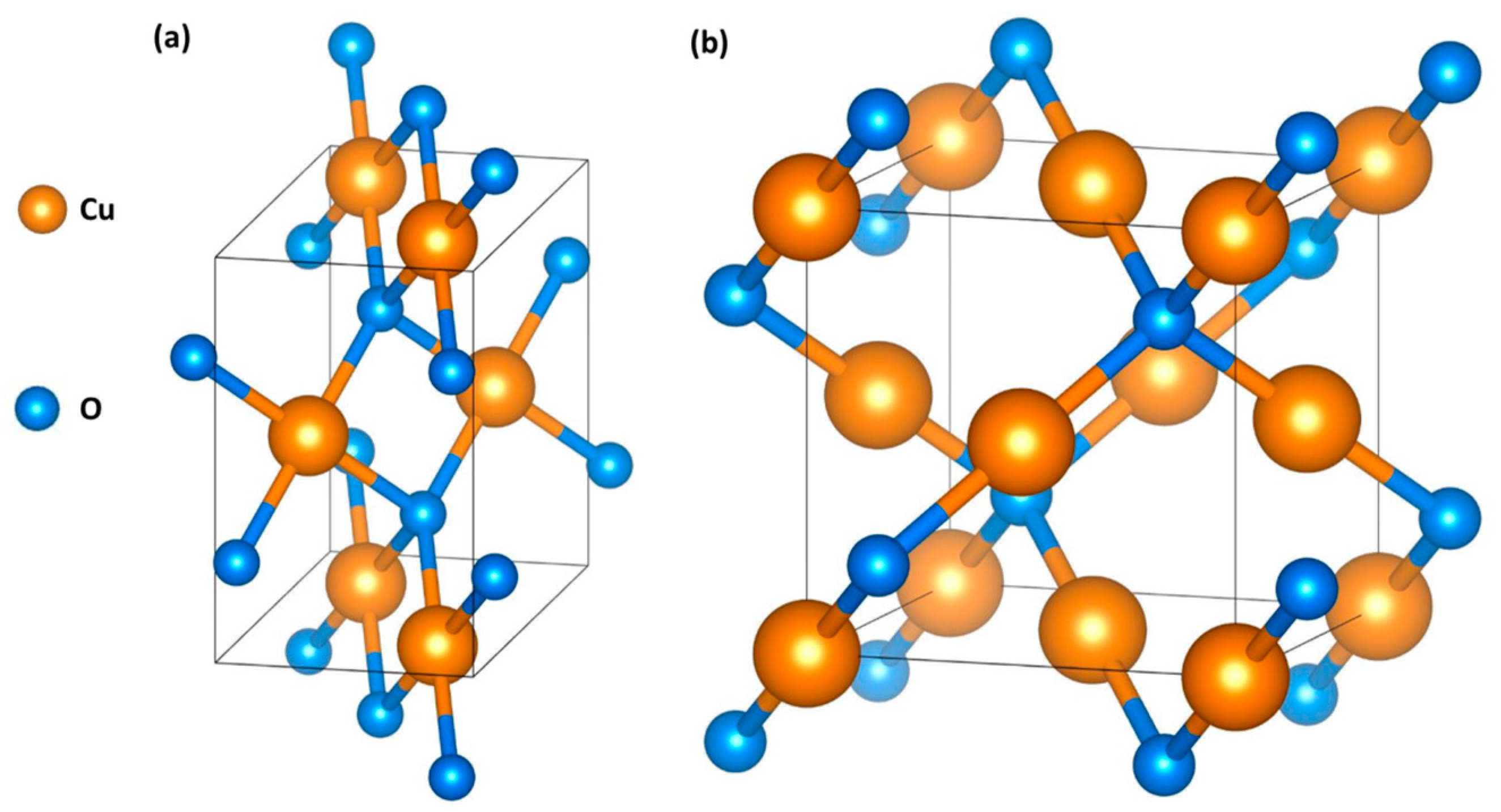
2.3. Copper Oxides
3. Summary and Perspectives
Funding
Conflicts of Interest
References
- Lewis, B.G.; Paine, D.C. Applications and processing of transparent conducting oxides. MRS Bull. 2000, 25, 22–27. [Google Scholar] [CrossRef]
- Fortunato, E.; Barquinha, P.; Martins, R. Oxide semiconductor thin-film transistors: A review of recent advances. Adv. Mater. 2012, 24, 2945–2986. [Google Scholar] [CrossRef] [PubMed]
- Fortunato, E.M.; Barquinha, P.M.; Pimentel, A.; Goncalves, A.M.; Marques, A.J.; Pereira, L.M.; Martins, R.F. Fully transparent zno thin-film transistor produced at room temperature. Adv. Mater. 2005, 17, 590–594. [Google Scholar] [CrossRef]
- Hoel, C.A.; Mason, T.O.; Gaillard, J.-F.; Poeppelmeier, K.R. Transparent conducting oxides in the ZnO-In2O3-SnO2 system. Chem. Mater. 2010, 22, 3569–3579. [Google Scholar] [CrossRef]
- Granqvist, C.G.; Hultåker, A. Transparent and conducting ito films: New developments and applications. Thin Solid Films 2002, 411, 1–5. [Google Scholar] [CrossRef]
- Niu, C. Carbon nanotube transparent conducting films. MRS Bull. 2011, 36, 766–773. [Google Scholar] [CrossRef]
- Chen, Z.; Li, W.; Li, R.; Zhang, Y.; Xu, G.; Cheng, H. Fabrication of highly transparent and conductive indium–tin oxide thin films with a high figure of merit via solution processing. Langmuir 2013, 29, 13836–13842. [Google Scholar] [CrossRef]
- Tripathi, T.S.; Karppinen, M. Atomic layer deposition of p-type semiconducting thin films: A review. Adv. Mater. Interfaces 2017, 4, 1700300. [Google Scholar] [CrossRef]
- Raebiger, H.; Lany, S.; Zunger, A. Origins of the p-type nature and cation deficiency in Cu2O and related materials. Phys. Rev. B 2007, 76, 045209. [Google Scholar] [CrossRef]
- Scanlon, D.O.; Watson, G.W. (Cu2S2)(Sr3Sc2O5)—A layered, direct band gap, p-type transparent conducting oxychalcogenide: A theoretical analysis. Chem. Mater. 2009, 21, 5435–5442. [Google Scholar] [CrossRef]
- Banerjee, A.; Chattopadhyay, K. Recent developments in the emerging field of crystalline p-type transparent conducting oxide thin films. Prog. Cryst. Growth Charact. Mater. 2005, 50, 52–105. [Google Scholar] [CrossRef]
- Hautier, G.; Miglio, A.; Ceder, G.; Rignanese, G.-M.; Gonze, X. Identification and design principles of low hole effective mass p-type transparent conducting oxides. Nat. Commun. 2013, 4, 2292. [Google Scholar] [CrossRef] [PubMed]
- Hiramatsu, H.; Kamiya, T.; Tohei, T.; Ikenaga, E.; Mizoguchi, T.; Ikuhara, Y.; Kobayashi, K.; Hosono, H. Origins of hole doping and relevant optoelectronic properties of wide gap p-type semiconductor, lacuose. J. Am. Chem. Soc. 2010, 132, 15060–15067. [Google Scholar] [CrossRef] [PubMed]
- Zakutayev, A.; McIntyre, D.; Schneider, G.; Kykyneshi, R.; Keszler, D.; Park, C.-H.; Tate, J. Tunable properties of wide-band gap p-type bacu (Ch1−xChx′)F (Ch = S, Se, Te) thin-film solid solutions. Thin Solid Films 2010, 518, 5494–5500. [Google Scholar] [CrossRef]
- Wijeyasinghe, N.; Regoutz, A.; Eisner, F.; Du, T.; Tsetseris, L.; Lin, Y.H.; Faber, H.; Pattanasattayavong, P.; Li, J.; Yan, F. Copper(I) thiocyanate (CuSCN) hole-transport layers processed from aqueous precursor solutions and their application in thin-film transistors and highly efficient organic and organometal halide perovskite solar cells. Adv. Funct. Mater. 2017, 27, 1701818. [Google Scholar] [CrossRef]
- Liu, X.; Zhang, N.; Tang, B.; Li, M.; Zhang, Y.-W.; Yu, Z.G.; Gong, H. Highly stable new organic–inorganic hybrid 3D perovskite CH3NH3PdI3 and 2D perovskite (CH3NH3)3Pd2I7: DFT analysis, synthesis, structure, transition behavior, and physical properties. J. Phys. Chem. Lett. 2018, 9, 5862–5872. [Google Scholar] [CrossRef] [PubMed]
- Liu, X.; Li, B.; Zhang, N.; Yu, Z.; Sun, K.; Tang, B.; Shi, D.; Yao, H.; Ouyang, J.; Gong, H. Multifunctional RbCl dopants for efficient inverted planar perovskite solar cell with ultra-high fill factor, negligible hysteresis and improved stability. Nano Energy 2018, 53, 567–578. [Google Scholar] [CrossRef]
- Liu, X.; Huang, T.J.; Zhang, L.; Tang, B.; Zhang, N.; Shi, D.; Gong, H. Highly stable, new, organic-inorganic perovskite (CH3NH3)2PdBr4: Synthesis, structure, and physical properties. Chem. Eur. J. 2018, 24, 4991–4998. [Google Scholar] [CrossRef] [PubMed]
- Klauk, H.; Zschieschang, U.; Pflaum, J.; Halik, M. Ultralow-power organic complementary circuits. Nature 2007, 445, 745. [Google Scholar] [CrossRef]
- Martins, R.; Nathan, A.; Barros, R.; Pereira, L.; Barquinha, P.; Correia, N.; Costa, R.; Ahnood, A.; Ferreira, I.; Fortunato, E. Complementary metal oxide semiconductor technology with and on paper. Adv. Mater. 2011, 23, 4491–4496. [Google Scholar] [CrossRef]
- Martins, R.F.; Ahnood, A.; Correia, N.; Pereira, L.M.; Barros, R.; Barquinha, P.M.; Costa, R.; Ferreira, I.M.; Nathan, A.; Fortunato, E.E. Recyclable, flexible, low-power oxide electronics. Adv. Funct. Mater. 2013, 23, 2153–2161. [Google Scholar] [CrossRef]
- Wager, J.F.; Hoffman, R. Thin, fast, and flexible. IEEE Spectr. 2011, 48, 42–56. [Google Scholar] [CrossRef]
- Kawazoe, H.; Yanagi, H.; Ueda, K.; Hosono, H. Transparent p-type conducting oxides: Design and fabrication of pn heterojunctions. MRS Bull. 2000, 25, 28–36. [Google Scholar] [CrossRef]
- Kawazoe, H.; Yasukawa, M.; Hyodo, H.; Kurita, M.; Yanagi, H.; Hosono, H. p-type electrical conduction in transparent thin films of CuAlO2. Nature 1997, 389, 939. [Google Scholar] [CrossRef]
- Hu, Z.; Huang, X.; Annapureddy, H.V.; Margulis, C.J. Molecular dynamics study of the temperature-dependent optical kerr effect spectra and intermolecular dynamics of room temperature ionic liquid 1-methoxyethylpyridinium dicyanoamide. J. Phys. Chem. B 2008, 112, 7837–7849. [Google Scholar] [CrossRef] [PubMed]
- Gong, H.; Wang, Y.; Luo, Y. Nanocrystalline p-type transparent Cu–Al–O semiconductor prepared by chemical-vapor deposition with Cu(acac)2 and Al(acac)3 precursors. Appl. Phys. Lett. 2000, 76, 3959–3961. [Google Scholar] [CrossRef]
- Ohashi, M.; Iida, Y.; Morikawa, H. Preparation of CuAlO2 films by wet chemical synthesis. J. Am. Ceram. Soc. 2002, 85, 270–272. [Google Scholar] [CrossRef]
- Banerjee, A.; Kundoo, S.; Chattopadhyay, K. Synthesis and characterization of p-type transparent conducting CuAlO2 thin film by dc sputtering. Thin Solid Films 2003, 440, 5–10. [Google Scholar] [CrossRef]
- Mahapatra, S.; Shivashankar, S.A. Low-pressure metal–organic chemical vapor deposition of transparent and p-type conducting CuCrO2 thin films with high conductivity. Chem. Vap. Depos. 2003, 9, 238–240. [Google Scholar] [CrossRef]
- Nagarajan, R.; Draeseke, A.; Sleight, A.; Tate, J. p-Type conductivity in CuCr1−xMgxO2 films and powders. J. Appl. Phys. 2001, 89, 8022–8025. [Google Scholar] [CrossRef]
- Bywalez, R.; Götzendörfer, S.; Löbmann, P. Structural and physical effects of Mg-doping on p-type CuCrO2 and CuAl0.5Cr0.5O2 thin films. J. Mater. Chem. 2010, 20, 6562–6570. [Google Scholar] [CrossRef]
- Ueda, K.; Hase, T.; Yanagi, H.; Kawazoe, H.; Hosono, H.; Ohta, H.; Orita, M.; Hirano, M. Epitaxial growth of transparent p-type conducting CuGaO2 thin films on sapphire (001) substrates by pulsed laser deposition. J. Appl. Phys. 2001, 89, 1790–1793. [Google Scholar] [CrossRef]
- Yanagi, H.; Kawazoe, H.; Kudo, A.; Yasukawa, M.; Hosono, H. Chemical design and thin film preparation of p-type conductive transparent oxides. J. Electroceram. 2000, 4, 407–414. [Google Scholar] [CrossRef]
- Srinivasan, R.; Chavillon, B.; Doussier-Brochard, C.; Cario, L.; Paris, M.; Gautron, E.; Deniard, P.; Odobel, F.; Jobic, S. Tuning the size and color of the p-type wide band gap delafossite semiconductor CuGaO2 with ethylene glycol assisted hydrothermal synthesis. J. Mater. Chem. 2008, 18, 5647–5653. [Google Scholar] [CrossRef]
- Yanagi, H.; Hase, T.; Ibuki, S.; Ueda, K.; Hosono, H. Bipolarity in electrical conduction of transparent oxide semiconductor CuInO2 with delafossite structure. Appl. Phys. Lett. 2001, 78, 1583–1585. [Google Scholar] [CrossRef]
- Sasaki, M.; Shimode, M. Fabrication of bipolar CuInO2 with delafossite structure. J. Phys. Chem. Solids 2003, 64, 1675–1679. [Google Scholar] [CrossRef]
- Yanagi, H.; Ueda, K.; Ohta, H.; Orita, M.; Hirano, M.; Hosono, H. Fabrication of all oxide transparent p–n homojunction using bipolar CuInO2 semiconducting oxide with delafossite structure. Solid State Commun. 2001, 121, 15–17. [Google Scholar] [CrossRef]
- Duan, N.; Sleight, A.; Jayaraj, M.; Tate, J. Transparent p-type conducting CuScO2+x films. Appl. Phys. Lett. 2000, 77, 1325–1326. [Google Scholar] [CrossRef]
- Kakehi, Y.; Nakao, S.; Satoh, K.; Yotsuya, T. Properties of copper-scandium oxide thin films prepared by pulsed laser deposition. Thin Solid Films 2003, 445, 294–298. [Google Scholar] [CrossRef]
- Kakehi, Y.; Satoh, K.; Yotsuya, T.; Nakao, S.; Yoshimura, T.; Ashida, A.; Fujimura, N. Epitaxial growth of CuScO2 thin films on sapphire a-plane substrates by pulsed laser deposition. J. Appl. Phys. 2005, 97, 083535. [Google Scholar] [CrossRef]
- Manoj, R.; Nisha, M.; Vanaja, K.; Jayaraj, M. Effect of oxygen intercalation on properties of sputtered CuYO2 for potential use as p-type transparent conducting films. Bull. Mater. Sci. 2008, 31, 49–53. [Google Scholar] [CrossRef]
- Nagarajan, R.; Duan, N.; Jayaraj, M.; Li, J.; Vanaja, K.; Yokochi, A.; Draeseke, A.; Tate, J.; Sleight, A. p-type conductivity in the delafossite structure. Int. J. Inorg. Mater. 2001, 3, 265–270. [Google Scholar] [CrossRef]
- Ingram, B.J.; González, G.B.; Mason, T.O.; Shahriari, D.Y.; Barnabe, A.; Ko, D.; Poeppelmeier, K.R. Transport and defect mechanisms in cuprous delafossites. 1. Comparison of hydrothermal and standard solid-state synthesis in CuAlO2. Chem. Mater. 2004, 16, 5616–5622. [Google Scholar] [CrossRef]
- Chen, H.-Y.; Wu, J.-H. Characterization and optoelectronic properties of sol–gel-derived CuFeO2 thin films. Thin Solid Films 2012, 520, 5029–5035. [Google Scholar] [CrossRef]
- Chiu, T.-W.; Huang, P.-S. Preparation of delafossite CuFeO2 coral-like powder using a self-combustion glycine nitrate process. Ceram. Int. 2013, 39, S575–S578. [Google Scholar] [CrossRef]
- Moharam, M.; Rashad, M.; Elsayed, E.; Abou-Shahba, R. A facile novel synthesis of delafossite CuFeO2 powders. J. Mater. Sci. Mater. Electron. 2014, 25, 1798–1803. [Google Scholar] [CrossRef]
- Snure, M.; Tiwari, A. CuBO2: A p-type transparent oxide. Appl. Phys. Lett. 2007, 91, 092123. [Google Scholar] [CrossRef]
- Santra, S.; Das, N.; Chattopadhyay, K. Physical and optical properties of CuBO2 nanopowders synthesized via sol-gel route. In Proceedings of the 16th International Workshop on Physics of Semiconductor Devices, Kanpur, India, 19–22 December 2011; p. 85491W. [Google Scholar]
- Iozzi, M.; Vajeeston, P.; Vidya, R.; Ravindran, P.; Fjellvåg, H. Structural and electronic properties of transparent conducting delafossite: A comparison between the AgBO2 and CuBO2 families (B = Al, Ga, In and Sc, Y). RSC Adv. 2015, 5, 1366–1377. [Google Scholar] [CrossRef]
- Kudo, A.; Yanagi, H.; Hosono, H.; Kawazoe, H. SrCu2O2: A p-type conductive oxide with wide band gap. Appl. Phys. Lett. 1998, 73, 220–222. [Google Scholar] [CrossRef]
- Ohta, H.; Kawamura, K.-I.; Orita, M.; Hirano, M.; Sarukura, N.; Hosono, H. Current injection emission from a transparent p–n junction composed of p-SrCu2O2/n-ZnO. Appl. Phys. Lett. 2000, 77, 475–477. [Google Scholar] [CrossRef]
- Ohta, H.; Orita, M.; Hirano, M.; Hosono, H. Fabrication and characterization of ultraviolet-emitting diodes composed of transparent p–n heterojunction, p-SrCu2O2 and n-ZnO. J. Appl. Phys. 2001, 89, 5720–5725. [Google Scholar] [CrossRef]
- Kim, J.; Yamamoto, K.; Iimura, S.; Ueda, S.; Hosono, H. Electron affinity control of amorphous oxide semiconductors and its applicability to organic electronics. Adv. Mater. Interfaces 2018, 5, 1801307. [Google Scholar] [CrossRef]
- Zhang, H.; Wang, H.; Chen, W.; Jen, A.K.Y. CuGaO2: A promising inorganic hole-transporting material for highly efficient and stable perovskite solar cells. Adv. Mater. 2017, 29, 1604984. [Google Scholar] [CrossRef] [PubMed]
- Mryasov, O.; Freeman, A. Electronic band structure of indium tin oxide and criteria for transparent conducting behavior. Phys. Rev. B 2001, 64, 233111. [Google Scholar] [CrossRef]
- Scanlon, D.O.; Watson, G.W. Understanding the p-type defect chemistry of CuCrO2. J. Mater. Chem. 2011, 21, 3655–3663. [Google Scholar] [CrossRef]
- Ingram, B.; Mason, T.; Asahi, R.; Park, K.; Freeman, A. Electronic structure and small polaron hole transport of copper aluminate. Phys. Rev. B 2001, 64, 155114. [Google Scholar] [CrossRef]
- Shin, D.; Foord, J.; Egdell, R.; Walsh, A. Electronic structure of CuCrO2 thin films grown on Al2O3 (001) by oxygen plasma assisted molecular beam epitaxy. J. Appl. Phys. 2012, 112, 113718. [Google Scholar] [CrossRef]
- Zhang, Y.; Qiao, Z.-P.; Chen, X.-M. Microwave-assisted elemental direct reaction route to nanocrystalline copper chalcogenides cuse and Cu2Te. J. Mater. Chem. 2002, 12, 2747–2748. [Google Scholar] [CrossRef]
- Liu, M.L.; Wu, L.B.; Huang, F.Q.; Chen, L.D.; Ibers, J.A. Syntheses, crystal and electronic structure, and some optical and transport properties of lncuote (Ln = La, Ce, Nd). J. Solid State Chem. 2007, 180, 62–69. [Google Scholar] [CrossRef]
- Ueda, K.; Inoue, S.; Hosono, H.; Sarukura, N.; Hirano, M. Room-temperature excitons in wide-gap layered-oxysulfide semiconductor: Lacuos. Appl. Phys. Lett. 2001, 78, 2333–2335. [Google Scholar] [CrossRef]
- Ueda, K.; Hiramatsu, H.; Ohta, H.; Hirano, M.; Kamiya, T.; Hosono, H. Single-atomic-layered quantum wells built in wide-gap semiconductors LnCuOCh (Ln = lanthanide, Ch = chalcogen). Phys. Rev. B 2004, 69, 155305. [Google Scholar] [CrossRef]
- Hiramatsu, H.; Ueda, K.; Ohta, H.; Hirano, M.; Kikuchi, M.; Yanagi, H.; Kamiya, T.; Hosono, H. Heavy hole doping of epitaxial thin films of a wide gap p-type semiconductor, lacuose, and analysis of the effective mass. Appl. Phys. Lett. 2007, 91, 012104. [Google Scholar] [CrossRef]
- Li, B.; Akimoto, K.; Shen, A. Growth of Cu2O thin films with high hole mobility by introducing a low-temperature buffer layer. J. Cryst. Growth 2009, 311, 1102–1105. [Google Scholar] [CrossRef]
- De Jongh, P.; Vanmaekelbergh, D.; Kelly, J. Cu2O: Electrodeposition and characterization. Chem. Mater. 1999, 11, 3512–3517. [Google Scholar] [CrossRef]
- Wang, Y.; Miska, P.; Pilloud, D.; Horwat, D.; Mücklich, F.; Pierson, J.-F. Transmittance enhancement and optical band gap widening of Cu2O thin films after air annealing. J. Appl. Phys. 2014, 115, 073505. [Google Scholar] [CrossRef]
- Nian, J.-N.; Hu, C.-C.; Teng, H. Electrodeposited p-type Cu2O for H2 evolution from photoelectrolysis of water under visible light illumination. Int. J. Hydrog. Energy 2008, 33, 2897–2903. [Google Scholar] [CrossRef]
- Ruiz, E.; Alvarez, S.; Alemany, P.; Evarestov, R.A. Electronic structure and properties of Cu2O. Phys. Rev. B 1997, 56, 7189. [Google Scholar] [CrossRef]
- Scanlon, D.O.; Morgan, B.J.; Watson, G.W.; Walsh, A. Acceptor levels in p-type Cu2O: Rationalizing theory and experiment. Phys. Rev. Lett. 2009, 103, 096405. [Google Scholar] [CrossRef]
- Ishiguro, T.; Kitazawa, A.; Mizutani, N.; Kato, M. Single-crystal growth and crystal structure refinement of CuAlO2. J. Solid State Chem. 1981, 40, 170–174. [Google Scholar] [CrossRef]
- Marquardt, M.A.; Ashmore, N.A.; Cann, D.P. Crystal chemistry and electrical properties of the delafossite structure. Thin Solid Films 2006, 496, 146–156. [Google Scholar] [CrossRef]
- Wei, R.; Tang, X.; Hu, L.; Yang, J.; Zhu, X.; Song, W.; Dai, J.; Zhu, X.; Sun, Y. Facile chemical solution synthesis of p-type delafossite Ag-based transparent conducting AgCrO2 films in an open condition. J. Mater. Chem. C 2017, 5, 1885–1892. [Google Scholar] [CrossRef]
- Benko, F.; Koffyberg, F. The optical interband transitions of the semiconductor CuGaO2. Physica Status Solidi (a) 1986, 94, 231–234. [Google Scholar] [CrossRef]
- Vanaja, K.; Ajimsha, R.; Asha, A.; Jayaraj, M. p-type electrical conduction in α-AgGaO2 delafossite thin films. Appl. Phys. Lett. 2006, 88, 212103. [Google Scholar] [CrossRef]
- Kandpal, H.C.; Seshadri, R. First-principles electronic structure of the delafossites ABO2 (A= Cu, Ag, Au; B= Al, Ga, Sc, In, Y): Evolution of d10–d10 interactions. Solid State Sci. 2002, 4, 1045–1052. [Google Scholar] [CrossRef]
- Huda, M.N.; Yan, Y.; Walsh, A.; Wei, S.-H.; Al-Jassim, M.M. Group-IIIA versus IIIB delafossites: Electronic structure study. Phys. Rev. B 2009, 80, 035205. [Google Scholar] [CrossRef]
- Pellicer-Porres, J.; Segura, A.; Gilliland, A.; Munoz, A.; Rodríguez-Hernández, P.; Kim, D.; Lee, M.; Kim, T. On the band gap of CuAlO2 delafossite. Appl. Phys. Lett. 2006, 88, 181904. [Google Scholar] [CrossRef]
- Gilliland, S.; Pellicer-Porres, J.; Segura, A.; Muñoz, A.; Rodríguez-Hernández, P.; Kim, D.; Lee, M.; Kim, T. Electronic structure of CuAlO2 and CuScO2 delafossites under pressure. Phys. Status Solidi (b) 2007, 244, 309–314. [Google Scholar] [CrossRef]
- Jayalakshmi, V.; Murugan, R.; Palanivel, B. Electronic and structural properties of CuMO2 (M = Al, Ga, In). J. Alloy. Compd. 2005, 388, 19–22. [Google Scholar] [CrossRef]
- Buljan, A.; Alemany, P.; Ruiz, E. Electronic structure and bonding in CuMO2 (M = Al, Ga, Y) delafossite-type oxides: An ab initio study. J. Phys. Chem. B 1999, 103, 8060–8066. [Google Scholar] [CrossRef]
- Schiavo, E.; Latouche, C.; Barone, V.; Crescenzi, O.; Muñoz-García, A.B.; Pavone, M. An ab initio study of Cu-based delafossites as an alternative to nickel oxide in photocathodes: Effects of Mg-doping and surface electronic features. Phys. Chem. Chem. Phys. 2018, 20, 14082–14089. [Google Scholar] [CrossRef] [PubMed]
- Sakulkalavek, A.; Sakdanuphab, R. Power factor improvement of delafossite CuAlO2 by liquid-phase sintering with Ag2O addition. Mater. Sci. Semicond. Process. 2016, 56, 313–323. [Google Scholar] [CrossRef]
- Li, J.; Sleight, A.; Jones, C.; Toby, B. Trends in negative thermal expansion behavior for AMO2 (A = Cu Or Ag; M = Al, Sc, In, or La) compounds with the delafossite structure. J. Solid State Chem. 2005, 178, 285–294. [Google Scholar] [CrossRef]
- Tsuboi, N.; Hoshino, T.; Ohara, H.; Suzuki, T.; Kobayashi, S.; Kato, K.; Kaneko, F. Control of luminescence and conductivity of delafossite-type CuYO2 by substitution of rare earth cation (Eu, Tb) and/or Ca cation for Y cation. J. Phys. Chem. Solids 2005, 66, 2134–2138. [Google Scholar] [CrossRef]
- Ruttanapun, C. Optical and electronic properties of delafossite CuBO2 p-type transparent conducting oxide. J. Appl. Phys. 2013, 114, 113108. [Google Scholar] [CrossRef]
- Scanlon, D.O.; Walsh, A.; Watson, G.W. Understanding the p-type conduction properties of the transparent conducting oxide CuBO2: A density functional theory analysis. Chem. Mater. 2009, 21, 4568–4576. [Google Scholar] [CrossRef]
- Scanlon, D.O.; Watson, G.W. Conductivity limits in CuAlO2 from screened-hybrid density functional theory. J. Phys. Chem. Lett. 2010, 1, 3195–3199. [Google Scholar] [CrossRef]
- Benko, F.; Koffyberg, F. Opto-electronic properties of CuAlO2. J. Phys. Chem. Solids 1984, 45, 57–59. [Google Scholar] [CrossRef]
- Fang, M.; He, H.; Lu, B.; Zhang, W.; Zhao, B.; Ye, Z.; Huang, J. Optical properties of p-type CuAlO2 thin film grown by rf magnetron sputtering. Appl. Surf. Sci. 2011, 257, 8330–8333. [Google Scholar] [CrossRef]
- Tsuboi, N.; Takahashi, Y.; Kobayashi, S.; Shimizu, H.; Kato, K.; Kaneko, F. Delafossite CuAlO2 films prepared by reactive sputtering using Cu and Al targets. J. Phys. Chem. Solids 2003, 64, 1671–1674. [Google Scholar] [CrossRef]
- Stauber, R.; Perkins, J.D.; Parilla, P.A.; Ginley, D.S. Thin film growth of transparent p-type CuAlO2. Electrochem. Solid-State Lett. 1999, 2, 654–656. [Google Scholar] [CrossRef]
- Tripathi, T.; Niemelä, J.-P.; Karppinen, M. Atomic layer deposition of transparent semiconducting oxide CuCrO2 thin films. J. Mater. Chem. C 2015, 3, 8364–8371. [Google Scholar] [CrossRef]
- Tripathi, T.S.; Karppinen, M. Enhanced p-type transparent semiconducting characteristics for ALD-grown Mg-substituted CuCrO2 thin films. Adv. Electron. Mater. 2017, 3, 1600341. [Google Scholar] [CrossRef]
- Gao, S.; Zhao, Y.; Gou, P.; Chen, N.; Xie, Y. Preparation of CuAlO2 nanocrystalline transparent thin films with high conductivity. Nanotechnology 2003, 14, 538. [Google Scholar] [CrossRef]
- Sheets, W.C.; Mugnier, E.; Barnabe, A.; Marks, T.J.; Poeppelmeier, K.R. Hydrothermal synthesis of delafossite-type oxides. Chem. Mater. 2006, 18, 7–20. [Google Scholar] [CrossRef]
- Götzendörfer, S.; Polenzky, C.; Ulrich, S.; Löbmann, P. Preparation of CuAlO2 and CuCrO2 thin films by sol–gel processing. Thin Solid Films 2009, 518, 1153–1156. [Google Scholar] [CrossRef]
- Prévot, M.S.; Li, Y.; Guijarro, N.; Sivula, K. Improving charge collection with delafossite photocathodes: A host–guest CuAlO2/CuFeO2 approach. J. Mater. Chem. A 2016, 4, 3018–3026. [Google Scholar] [CrossRef]
- Chiu, S.; Huang, J. Characterization of p-type CuAlO2 thin films grown by chemical solution deposition. Surf. Coat. Technol. 2013, 231, 239–242. [Google Scholar] [CrossRef]
- Phani, P.S.; Vishnukanthan, V.; Sundararajan, G. Effect of heat treatment on properties of cold sprayed nanocrystalline copper alumina coatings. Acta Mater. 2007, 55, 4741–4751. [Google Scholar] [CrossRef]
- Bouzidi, C.; Bouzouita, H.; Timoumi, A.; Rezig, B. Fabrication and characterization of CuAlO2 transparent thin films prepared by spray technique. Mater. Sci. Eng. B 2005, 118, 259–263. [Google Scholar] [CrossRef]
- Grilli, M.; Menchini, F.; Dikonimos, T.; Nunziante, P.; Pilloni, L.; Yilmaz, M.; Piegari, A.; Mittiga, A. Effect of growth parameters on the properties of RF-sputtered highly conductive and transparent p-type NiOx films. Semicond. Sci. Technol. 2016, 31, 055016. [Google Scholar] [CrossRef]
- Lu, Y.; He, Y.; Yang, B.; Polity, A.; Volbers, N.; Neumann, C.; Hasselkamp, D.; Meyer, B. RF reactive sputter deposition and characterization of transparent CuAlO2 thin films. Phys. Status Solidi c 2006, 3, 2895–2898. [Google Scholar] [CrossRef]
- Zhang, K.H.; Xi, K.; Blamire, M.G.; Egdell, R.G. P-type transparent conducting oxides. J. Phys. Condens. Matter 2016, 28, 383002. [Google Scholar] [CrossRef] [PubMed]
- Xiao, B.; Ye, Z.; Zhang, Y.; Zeng, Y.; Zhu, L.; Zhao, B. Fabrication of p-type Li-doped ZnO films by pulsed laser deposition. Appl. Surf. Sci. 2006, 253, 895–897. [Google Scholar] [CrossRef]
- Ryu, Y.; Kim, W.; White, H. Fabrication of homostructural ZnO p–n junctions. J. Cryst. Growth 2000, 219, 419–422. [Google Scholar] [CrossRef]
- Leskelä, M.; Ritala, M. Atomic layer deposition chemistry: Recent developments and future challenges. Angew. Chem. Int. Ed. 2003, 42, 5548–5554. [Google Scholar] [CrossRef] [PubMed]
- Miikkulainen, V.; Leskelä, M.; Ritala, M.; Puurunen, R.L. Crystallinity of inorganic films grown by atomic layer deposition: Overview and general trends. J. Appl. Phys. 2013, 113, 2. [Google Scholar] [CrossRef]
- Das, B.; Renaud, A.; Volosin, A.M.; Yu, L.; Newman, N.; Seo, D.-K. Nanoporous delafossite CuAlO2 from inorganic/polymer double gels: A desirable high-surface-area p-type transparent electrode material. Inorg. Chem. 2015, 54, 1100–1108. [Google Scholar] [CrossRef] [PubMed]
- Nie, S.; Liu, A.; Meng, Y.; Shin, B.; Liu, G.; Shan, F. Solution-processed ternary p-type CuCrO2 semiconductor thin films and their application in transistors. J. Mater. Chem. C 2018, 6, 1393–1398. [Google Scholar] [CrossRef]
- Ginley, D.; Roy, B.; Ode, A.; Warmsingh, C.; Yoshida, Y.; Parilla, P.; Teplin, C.; Kaydanova, T.; Miedaner, A.; Curtis, C. Non-vacuum and pld growth of next generation tco materials. Thin Solid Films 2003, 445, 193–198. [Google Scholar] [CrossRef]
- Yanagi, H.; Inoue, S.-I.; Ueda, K.; Kawazoe, H.; Hosono, H.; Hamada, N. Electronic structure and optoelectronic properties of transparent p-type conducting CuAlO2. J. Appl. Phys. 2000, 88, 4159–4163. [Google Scholar] [CrossRef]
- Aston, D.; Payne, D.; Green, A.; Egdell, R.; Law, D.; Guo, J.; Glans, P.; Learmonth, T.; Smith, K. High-resolution X-ray spectroscopic study of the electronic structure of the prototypical p-type transparent conducting oxide CuAlO2. Phys. Rev. B 2005, 72, 195115. [Google Scholar] [CrossRef]
- Katayama-Yoshida, H.; Koyanagi, T.; Funashima, H.; Harima, H.; Yanase, A. Engineering of nested fermi surface and transparent conducting p-type delafossite CuAlO2: Possible lattice instability or transparent superconductivity? Solid State Commun. 2003, 126, 135–139. [Google Scholar] [CrossRef]
- Koyanagi, T.; Harima, H.; Yanase, A.; Katayama-Yoshida, H. Materials design of p-type transparent conducting oxides of delafossite CuAlO2 by super-cell FLAPW method. J. Phys. Chem. Solids 2003, 64, 1443–1446. [Google Scholar] [CrossRef]
- Dong, G.; Zhang, M.; Lan, W.; Dong, P.; Yan, H. Structural and physical properties of Mg-doped CuAlO2 thin films. Vacuum 2008, 82, 1321–1324. [Google Scholar] [CrossRef]
- Durá, O.; Boada, R.; Rivera-Calzada, A.; León, C.; Bauer, E.; de la Torre, M.L.; Chaboy, J. Transport, electronic, and structural properties of nanocrystalline CuAlO2 delafossites. Phys. Rev. B 2011, 83, 045202. [Google Scholar] [CrossRef]
- Lee, M.; Kim, T.; Kim, D. Anisotropic electrical conductivity of delafossite-type CuAlO2 laminar crystal. Appl. Phys. Lett. 2001, 79, 2028–2030. [Google Scholar] [CrossRef]
- Tate, J.; Ju, H.; Moon, J.; Zakutayev, A.; Richard, A.; Russell, J.; McIntyre, D. Origin of p-type conduction in single-crystal CuAlO2. Phys. Rev. B 2009, 80, 165206. [Google Scholar] [CrossRef]
- Luo, J.; Lin, Y.-J.; Hung, H.-C.; Liu, C.-J.; Yang, Y.-W. Tuning the formation of p-type defects by peroxidation of CuAlO2 films. J. Appl. Phys. 2013, 114, 033712. [Google Scholar]
- Yao, Z.; He, B.; Zhang, L.; Zhuang, C.; Ng, T.; Liu, S.; Vogel, M.; Kumar, A.; Zhang, W.; Lee, C. Energy band engineering and controlled p-type conductivity of CuAlO2 thin films by nonisovalent Cu–O alloying. Appl. Phys. Lett. 2012, 100, 062102. [Google Scholar] [CrossRef]
- Rastogi, A.; Lim, S.; Desu, S. Structure and optoelectronic properties of spray deposited Mg doped p-CuCrO2 semiconductor oxide thin films. J. Appl. Phys. 2008, 104, 023712. [Google Scholar] [CrossRef]
- Chen, H.-Y.; Yang, C.-C. Transparent p-type Zn-doped CuCrO2 films by sol–gel processing. Surf. Coat. Technol. 2013, 231, 277–280. [Google Scholar] [CrossRef]
- Dong, G.; Zhang, M.; Zhao, X.; Yan, H.; Tian, C.; Ren, Y. Improving the electrical conductivity of CuCrO2 thin film by n doping. Appl. Surf. Sci. 2010, 256, 4121–4124. [Google Scholar] [CrossRef]
- Ahmadi, M.; Asemi, M.; Ghanaatshoar, M. Mg and N co-doped CuCrO2: A record breaking p-type TCO. Appl. Phys. Lett. 2018, 113, 242101. [Google Scholar] [CrossRef]
- Crêpellière, J.; Popa, P.L.; Bahlawane, N.; Leturcq, R.; Werner, F.; Siebentritt, S.; Lenoble, D. Transparent conductive CuCrO2 thin films deposited by pulsed injection metal organic chemical vapor deposition: Up-scalable process technology for an improved transparency/conductivity trade-off. J. Mater. Chem. C 2016, 4, 4278–4287. [Google Scholar] [CrossRef]
- Popa, P.L.; Crepelliere, J.; Nukala, P.; Leturcq, R.; Lenoble, D. Invisible electronics: Metastable Cu-vacancies chain defects for highly conductive p-type transparent oxide. Appl. Mater. Today 2017, 9, 184–191. [Google Scholar] [CrossRef]
- Farrell, L.; Norton, E.; O’Dowd, B.; Caffrey, D.; Shvets, I.; Fleischer, K. Spray pyrolysis growth of a high figure of merit, nano-crystalline, p-type transparent conducting material at low temperature. Appl. Phys. Lett. 2015, 107, 031901. [Google Scholar] [CrossRef]
- Papadopoulou, E.; Viskadourakis, Z.; Pennos, A.; Huyberechts, G.; Aperathitis, E. The effect of deposition parameters on the properties of SrCu2O2 films fabricated by pulsed laser deposition. Thin Solid Films 2008, 516, 1449–1452. [Google Scholar] [CrossRef]
- Arnold, T.; Payne, D.; Bourlange, A.; Hu, J.; Egdell, R.; Piper, L.; Colakerol, L.; De Masi, A.; Glans, P.-A.; Learmonth, T. X-ray spectroscopic study of the electronic structure of CuCrO2. Phys. Rev. B 2009, 79, 075102. [Google Scholar] [CrossRef]
- Scanlon, D.O.; Walsh, A.; Morgan, B.J.; Watson, G.W.; Payne, D.J.; Egdell, R.G. Effect of cr substitution on the electronic structure of CuAl1−xCrxO2. Phys. Rev. B 2009, 79, 035101. [Google Scholar] [CrossRef]
- Scanlon, D.O.; Godinho, K.G.; Morgan, B.J.; Watson, G.W. Understanding conductivity anomalies in CuI-based delafossite transparent conducting oxides: Theoretical insights. J. Chem. Phys. 2010, 132, 024707. [Google Scholar] [CrossRef]
- Zheng, S.; Jiang, G.; Su, J.; Zhu, C. The structural and electrical property of CuCr1−xNixO2 delafossite compounds. Mater. Lett. 2006, 60, 3871–3873. [Google Scholar] [CrossRef]
- Kaya, I.C.; Sevindik, M.A.; Akyıldız, H. Characteristics of Fe-and Mg-doped CuCrO2 nanocrystals prepared by hydrothermal synthesis. J. Mater. Sci. Mater. Electron. 2016, 27, 2404–2411. [Google Scholar] [CrossRef]
- Okuda, T.; Jufuku, N.; Hidaka, S.; Terada, N. Magnetic, transport, and thermoelectric properties of the delafossite oxides CuCr1−xMgxO2 (0 ≤ x ≤ 0.04). Phys. Rev. B 2005, 72, 144403. [Google Scholar] [CrossRef]
- Madre, M.; Torres, M.; Gomez, J.; Diez, J.; Sotelo, A. Effect of alkaline earth dopant on density, mechanical, and electrical properties of Cu0.97AE0.03CrO2 (AE = Mg, Ca, Sr, and Ba) delafossite oxide. J. Aust. Ceram. Soc. 2019, 55, 257–263. [Google Scholar] [CrossRef]
- Xu, Y.; Nie, G.-Z.; Zou, D.; Tang, J.-W.; Ao, Z. N–Mg dual-acceptor co-doping in CuCrO2 studied by first-principles calculations. Phys. Lett. A 2016, 380, 3861–3865. [Google Scholar] [CrossRef]
- Mandal, P.; Mazumder, N.; Saha, S.; Ghorai, U.K.; Roy, R.; Das, G.C.; Chattopadhyay, K.K. A scheme of simultaneous cationic–anionic substitution in CuCrO2 for transparent and superior p-type transport. J. Phys. D Appl. Phys. 2016, 49, 275109. [Google Scholar] [CrossRef]
- Monteiro, J.F.H.L.; Monteiro, F.C.; Jurelo, A.R.; Mosca, D.H. Conductivity in (Ag,Mg)-doped delafossite oxide CuCrO2. Ceram. Int. 2018, 44, 14101–14107. [Google Scholar] [CrossRef]
- Wang, J.; Daunis, T.B.; Cheng, L.; Zhang, B.; Kim, J.; Hsu, J.W. Combustion synthesis of p-type transparent conducting CuCro2+x and Cu: Crox thin films at 180 °C. ACS Appl. Mater. Interfaces 2018, 10, 3732–3738. [Google Scholar] [CrossRef]
- Jun, T.; Kim, J.; Sasase, M.; Hosono, H. Material design of p-type transparent amorphous semiconductor, Cu–Sn–I. Adv. Mater. 2018, 30, 1706573. [Google Scholar] [CrossRef] [PubMed]
- Li, X.R.; Han, M.J.; Wu, J.D.; Shan, C.; Hu, Z.G.; Zhu, Z.Q.; Chu, J.H. Low voltage tunneling magnetoresistance in CuCrO2-based semiconductor heterojunctions at room temperature. J. Appl. Phys. 2014, 116, 223701. [Google Scholar] [CrossRef]
- Wang, J.; Lee, Y.-J.; Hsu, J.W. Sub-10 nm copper chromium oxide nanocrystals as a solution processed p-type hole transport layer for organic photovoltaics. J. Mater. Chem. C 2016, 4, 3607–3613. [Google Scholar] [CrossRef]
- Ngo, T.; Palstra, T.; Blake, G. Crystallite size dependence of thermoelectric performance of CuCrO2. RSC Adv. 2016, 6, 91171–91178. [Google Scholar] [CrossRef]
- Ono, Y.; Satoh, K.-I.; Nozaki, T.; Kajitani, T. Structural, magnetic and thermoelectric properties of delafossite-type oxide, CuCr1−xMgxO2 (0 ≤ x ≤ 0.05). Jpn. J. Appl. Phys. 2007, 46, 1071. [Google Scholar] [CrossRef]
- Li, X.; Han, M.; Zhang, X.; Shan, C.; Hu, Z.; Zhu, Z.; Chu, J. Temperature-dependent band gap, interband transitions, and exciton formation in transparent p-type delafossite CuCr1−xMgxO2 films. Phys. Rev. B 2014, 90, 035308. [Google Scholar] [CrossRef]
- Yokobori, T.; Okawa, M.; Konishi, K.; Takei, R.; Katayama, K.; Oozono, S.; Shinmura, T.; Okuda, T.; Wadati, H.; Sakai, E. Electronic structure of the hole-doped delafossite oxides CuCr1−xMgxO2. Phys. Rev. B 2013, 87, 195124. [Google Scholar] [CrossRef]
- Li, D.; Fang, X.; Deng, Z.; Zhou, S.; Tao, R.; Dong, W.; Wang, T.; Zhao, Y.; Meng, G.; Zhu, X. Electrical, optical and structural properties of CuCrO2 films prepared by pulsed laser deposition. J. Phys. D Appl. Phys. 2007, 40, 4910. [Google Scholar] [CrossRef]
- Benko, F.; Koffyberg, F. Preparation and opto-electronic properties of semiconducting CuCrO2. Mater. Res. Bull. 1986, 21, 753–757. [Google Scholar] [CrossRef]
- Nie, X.; Wei, S.-H.; Zhang, S. Bipolar doping and band-gap anomalies in delafossite transparent conductive oxides. Phys. Rev. Lett. 2002, 88, 066405. [Google Scholar] [CrossRef]
- Santra, S.; Das, N.; Chattopadhyay, K. Sol–gel synthesis and characterization of wide band gap p-type nanocrystalline CuBO2. Mater. Lett. 2013, 92, 198–201. [Google Scholar] [CrossRef]
- Santra, S.; Das, N.; Chattopadhyay, K. Wide band gap p-type nanocrystalline CuBO2 as a novel UV photocatalyst. Mater. Res. Bull. 2013, 48, 2669–2677. [Google Scholar] [CrossRef]
- Santra, S.; Das, N.S.; Chattopadhyay, K.K. CuBO2: A new photoconducting material. AIP Conf. Proc. 2013, 1536, 723–724. [Google Scholar] [CrossRef]
- Renaud, A.; Chavillon, B.; Le Pleux, L.; Pellegrin, Y.; Blart, E.; Boujtita, M.; Pauporte, T.; Cario, L.; Jobic, S.; Odobel, F. CuGaO2: A promising alternative for NiO in p-type dye solar cells. J. Mater. Chem. 2012, 22, 14353–14356. [Google Scholar] [CrossRef]
- Xu, Z.; Xiong, D.; Wang, H.; Zhang, W.; Zeng, X.; Ming, L.; Chen, W.; Xu, X.; Cui, J.; Wang, M. Remarkable photocurrent of p-type dye-sensitized solar cell achieved by size controlled CuGaO2 nanoplates. J. Mater. Chem. A 2014, 2, 2968–2976. [Google Scholar] [CrossRef]
- Yu, M.; Natu, G.; Ji, Z.; Wu, Y. p-type dye-sensitized solar cells based on delafossite CuGaO2 nanoplates with saturation photovoltages exceeding 460 mV. J. Phys. Chem. Lett. 2012, 3, 1074–1078. [Google Scholar] [CrossRef] [PubMed]
- Renaud, A.l.; Cario, L.; Deniard, P.; Gautron, E.; Rocquefelte, X.; Pellegrin, Y.; Blart, E.; Odobel, F.; Jobic, S. Impact of Mg doping on performances of CuGaO2 based p-type dye-sensitized solar cells. J. Phys. Chem. C 2013, 118, 54–59. [Google Scholar] [CrossRef]
- Zhang, S.; Wei, S.-H.; Zunger, A. A phenomenological model for systematization and prediction of doping limits in II–VI and I–III–VI2 compounds. J. Appl. Phys. 1998, 83, 3192–3196. [Google Scholar] [CrossRef]
- Zhang, S.; Wei, S.-H.; Zunger, A. Microscopic origin of the phenomenological equilibrium “doping limit rule” in n-type III-V semiconductors. Phys. Rev. Lett. 2000, 84, 1232. [Google Scholar] [CrossRef]
- Zhang, S.; Wei, S.-H.; Zunger, A. Intrinsic n-type versus p-type doping asymmetry and the defect physics of ZnO. Phys. Rev. B 2001, 63, 075205. [Google Scholar] [CrossRef]
- Arai, T.; Iimura, S.; Kim, J.; Toda, Y.; Ueda, S.; Hosono, H. Chemical design and example of transparent bipolar semiconductors. J. Am. Chem. Soc. 2017, 139, 17175–17180. [Google Scholar] [CrossRef]
- Cava, R.; Zandbergen, H.; Ramirez, A.; Takagi, H.; Chen, C.; Krajewski, J.; Peck, W., Jr.; Waszczak, J.; Meigs, G.; Roth, R. LaCuO25+x and YCuO2.5+x delafossites: Materials with triangular Cu2+δ planes. J. Solid State Chem. 1993, 104, 437–452. [Google Scholar] [CrossRef]
- Ingram, B.J.; Harder, B.J.; Hrabe, N.W.; Mason, T.O.; Poeppelmeier, K.R. Transport and defect mechanisms in cuprous delafossites. 2. CuScO2 and CuYO2. Chem. Mater. 2004, 16, 5623–5629. [Google Scholar] [CrossRef]
- Ohta, H.; Orita, M.; Hirano, M.; Yagi, I.; Ueda, K.; Hosono, H. Electronic structure and optical properties of SrCu2O2. J. Appl. Phys. 2002, 91, 3074–3078. [Google Scholar] [CrossRef]
- Kudo, A.; Yanagi, H.; Ueda, K.; Hosono, H.; Kawazoe, H.; Yano, Y. Fabrication of transparent p–n heterojunction thin film diodes based entirely on oxide semiconductors. Appl. Phys. Lett. 1999, 75, 2851–2853. [Google Scholar] [CrossRef]
- Ohta, H.; Kawamura, K.; Orita, M.; Sarukura, N.; Hirano, M.; Hosono, H. UV-emitting diode composed of transparent oxide semiconductors: p-SrCu2O2/n-ZnO. Electron. Lett 2000, 36, 984–985. [Google Scholar] [CrossRef]
- Hosono, H.; Ohta, H.; Hayashi, K.; Orita, M.; Hirano, M. Near-UV emitting diodes based on a transparent p–n junction composed of heteroepitaxially grown p-SrCu2O2 and n-ZnO. J. Cryst. Growth 2002, 237, 496–502. [Google Scholar] [CrossRef]
- Inoue, S.-I.; Ueda, K.; Hosono, H.; Hamada, N. Electronic structure of the transparent p-type semiconductor (LaO)CuS. Phys. Rev. B 2001, 64, 245211. [Google Scholar] [CrossRef]
- Ueda, K.; Inoue, S.; Hirose, S.; Kawazoe, H.; Hosono, H. Transparent p-type semiconductor: Lacuos layered oxysulfide. Appl. Phys. Lett. 2000, 77, 2701–2703. [Google Scholar] [CrossRef]
- Hiramatsu, H.; Ueda, K.; Ohta, H.; Orita, M.; Hirano, M.; Hosono, H. Preparation of transparent p-type (La1−xSrxO) cus thin films by RF sputtering technique. Thin Solid Films 2002, 411, 125–128. [Google Scholar] [CrossRef]
- Hiramatsu, H.; Ueda, K.; Takafuji, K.; Ohta, H.; Hirano, M.; Kamiyama, T.; Hosono, H. Intrinsic excitonic photoluminescence and band-gap engineering of wide-gap p-type oxychalcogenide epitaxial films of LnCuOCh (Ln = La, Pr, and Nd; Ch = S or Se) semiconductor alloys. J. Appl. Phys. 2003, 94, 5805–5808. [Google Scholar] [CrossRef]
- Ueda, K.; Hosono, H.; Hamada, N. Energy band structure of LnCuOCh (Ch = S, Se and Te) calculated by the full-potential linearized augmented plane-wave method. J. Phys. Condens. Matter 2004, 16, 5179. [Google Scholar] [CrossRef]
- Liu, M.-L.; Wu, L.-B.; Huang, F.-Q.; Chen, L.-D.; Chen, I.-W. A promising p-type transparent conducting material: Layered oxysulfide [Cu2S2][Sr3Sc2O5]. AIP J. Appl. Phys. 2007, 102, 116108. [Google Scholar] [CrossRef]
- Scanlon, D.O.; Buckeridge, J.; Catlow, C.R.A.; Watson, G.W. Understanding doping anomalies in degenerate p-type semiconductor lacuose. J. Mater. Chem. C 2014, 2, 3429–3438. [Google Scholar] [CrossRef]
- Ueda, K.; Takafuji, K.; Hiramatsu, H.; Ohta, H.; Kamiya, T.; Hirano, M.; Hosono, H. Electrical and optical properties and electronic structures of LnCuOS (Ln = La∼Nd). Chem. Mater. 2003, 15, 3692–3695. [Google Scholar] [CrossRef]
- Hiramatsu, H.; Ueda, K.; Ohta, H.; Hirano, M.; Kamiya, T.; Hosono, H. Degenerate p-type conductivity in wide-gap LaCuOS1−xSex (x = 0–1) epitaxial films. Appl. Phys. Lett. 2003, 82, 1048–1050. [Google Scholar] [CrossRef]
- Hiramatsu, H.; Yanagi, H.; Kamiya, T.; Ueda, K.; Hirano, M.; Hosono, H. Crystal structures, optoelectronic properties, and electronic structures of layered oxychalcogenides MCuOCh (M = Bi, La; Ch = S, Se, Te): Effects of electronic configurations of M3+ ions. Chem. Mater. 2007, 20, 326–334. [Google Scholar] [CrossRef]
- Ueda, K.; Hosono, H.; Hamada, N. Valence-band structures of layered oxychalcogenides, LaCuOCh (Ch = S, Se, and Te), studied by ultraviolet photoemission spectroscopy and energy-band calculations. J. Appl. Phys. 2005, 98, 043506. [Google Scholar] [CrossRef]
- Ueda, K.; Takafuji, K.; Yanagi, H.; Kamiya, T.; Hosono, H.; Hiramatsu, H.; Hirano, M.; Hamada, N. Optoelectronic properties and electronic structure of YCuOSe. J. Appl. Phys. 2007, 102, 113714. [Google Scholar] [CrossRef]
- Hiramatsu, H.; Orita, M.; Hirano, M.; Ueda, K.; Hosono, H. Electrical conductivity control in transparent p-type (LaO)CuS thin films prepared by rf sputtering. J. Appl. Phys. 2002, 91, 9177–9181. [Google Scholar] [CrossRef]
- Ueda, K.; Hosono, H. Band gap engineering, band edge emission, and p-type conductivity in wide-gap LaCuOS1−xSex oxychalcogenides. J. Appl. Phys. 2002, 91, 4768–4770. [Google Scholar] [CrossRef]
- Hiramatsu, H.; Ueda, K.; Ohta, H.; Orita, M.; Hirano, M.; Hosono, H. Heteroepitaxial growth of a wide-gap p-type semiconductor, LaCuOS. Appl. Phys. Lett. 2002, 81, 598–600. [Google Scholar] [CrossRef]
- Hamberg, I.; Granqvist, C.G. Evaporated Sn-doped In2O3 films: Basic optical properties and applications to energy-efficient windows. J. Appl. Phys. 1986, 60, R123–R160. [Google Scholar] [CrossRef]
- Slaoui, A.; Siffert, P. Determination of the electron effective mass and relaxation time in heavily doped silicon. Phys. Status Solidi (a) 1985, 89, 617–622. [Google Scholar] [CrossRef]
- Hosono, H. Built-in nanostructures in transparent oxides for novel photonic and electronic functions materials. Int. J. Appl. Ceram. Technol. 2004, 1, 106–118. [Google Scholar] [CrossRef]
- Moss, T. The interpretation of the properties of indium antimonide. Proc. Phys. Soc. Sect. B 1954, 67, 775. [Google Scholar] [CrossRef]
- Goto, Y.; Tanaki, M.; Okusa, Y.; Shibuya, T.; Yasuoka, K.; Matoba, M.; Kamihara, Y. Effects of the Cu off-stoichiometry on transport properties of wide gap p-type semiconductor, layered oxysulfide lacuso. Appl. Phys. Lett. 2014, 105, 022104. [Google Scholar] [CrossRef]
- Hiramatsu, H.; Ueda, K.; Ohta, H.; Kamiya, T.; Hirano, M.; Hosono, H. Excitonic blue luminescence from p-LaCuOSe/n-InGaZn5O8 light-emitting diode at room temperature. Appl. Phys. Lett. 2005, 87, 211107. [Google Scholar] [CrossRef]
- Yanagi, H.; Kikuchi, M.; Kim, K.-B.; Hiramatsu, H.; Kamiya, T.; Hirano, M.; Hosono, H. Low and small resistance hole-injection barrier for NPB realized by wide-gap p-type degenerate semiconductor, LaCuOSe:Mg. Org. Electron. 2008, 9, 890–894. [Google Scholar] [CrossRef]
- Zhang, N.; Liu, X.; Shi, D.; Tang, B.; Annadi, A.; Gong, H. Achievement of highly conductive p-type transparent ndcuos film with cu deficiency and effective doping. Mater. Today Chem. 2018, 10, 79–89. [Google Scholar] [CrossRef]
- Kremers, H.; Stevens, R. Observations on the rare earths. XIV. The preparation and properties of metallic lanthanum. J. Am. Chem. Soc. 1923, 45, 614–617. [Google Scholar] [CrossRef]
- Nakachi, Y.; Ueda, K. Single crystal growth of lacuos by the flux method. J. Cryst. Growth 2008, 311, 114–117. [Google Scholar] [CrossRef]
- Doussier-Brochard, C.; Chavillon, B.; Cario, L.; Jobic, S. Synthesis of p-type transparent LaOCuS nanoparticles via soft chemistry. Inorg. Chem. 2010, 49, 3074–3076. [Google Scholar] [CrossRef] [PubMed]
- Lian, J.; Li, N.; Wang, H.; Su, Y.; Zhang, G.; Liu, F. Synthesis of lacuos nanopowder by a novel precipitation combined with reduction route. Ceram. Int. 2016, 42, 11473–11477. [Google Scholar] [CrossRef]
- Zhang, N.; Gong, H. p-type transparent lacuos semiconductor synthesized via a novel two-step solid state reaction and sulfurization process. Ceram. Int. 2017, 43, 6295–6302. [Google Scholar] [CrossRef]
- Hiramatsu, H.; Ueda, K.; Ohta, H.; Hirano, M.; Kamiya, T.; Hosono, H. Wide gap p-type degenerate semiconductor: Mg-doped LaCuOSe. Thin Solid Films 2003, 445, 304–308. [Google Scholar] [CrossRef]
- Zhang, N.; Shi, D.; Liu, X.; Annadi, A.; Tang, B.; Huang, T.J.; Gong, H. High performance p-type transparent LaCuOS thin film fabricated through a hydrogen-free method. Appl. Mater. Today 2018, 13, 15–23. [Google Scholar] [CrossRef]
- Wang, Z.; Nayak, P.K.; Caraveo-Frescas, J.A.; Alshareef, H.N. Recent developments in p-type oxide semiconductor materials and devices. Adv. Mater. 2016, 28, 3831–3892. [Google Scholar] [CrossRef] [PubMed]
- Xu, W.; Li, H.; Xu, J.-B.; Wang, L. Recent advances of solution-processed metal oxide thin-film transistors. ACS Appl. Mater. Interfaces 2018, 10, 25878–25901. [Google Scholar] [CrossRef]
- Nolan, M.; Elliott, S.D. The p-type conduction mechanism in Cu2O: A first principles study. Phys. Chem. Chem. Phys. 2006, 8, 5350–5358. [Google Scholar] [CrossRef]
- Fortunato, E.; Figueiredo, V.; Barquinha, P.; Elamurugu, E.; Barros, R.; Gonçalves, G.; Park, S.-H.K.; Hwang, C.-S.; Martins, R. Thin-film transistors based on p-type Cu2O thin films produced at room temperature. Appl. Phys. Lett. 2010, 96, 192102. [Google Scholar] [CrossRef]
- Saji, K.J.; Populoh, S.; Tiwari, A.N.; Romanyuk, Y.E. Design of p-CuO/n-ZnO heterojunctions by rf magnetron sputtering. Phys. Status Solidi (a) 2013, 210, 1386–1391. [Google Scholar] [CrossRef]
- Chen, W.-C.; Hsu, P.-C.; Chien, C.-W.; Chang, K.-M.; Hsu, C.-J.; Chang, C.-H.; Lee, W.-K.; Chou, W.-F.; Hsieh, H.-H.; Wu, C.-C. Room-temperature-processed flexible n-InGaZnO/p-Cu2O heterojunction diodes and high-frequency diode rectifiers. J. Phys. D Appl. Phys. 2014, 47, 365101. [Google Scholar] [CrossRef]
- Dhakal, D.; Waechtler, T.; Schulz, S.E.; Gessner, T.; Lang, H.; Mothes, R.; Tuchscherer, A. Surface chemistry of a Cu(I) beta-diketonate precursor and the atomic layer deposition of Cu2O on SiO2 studied by X-ray photoelectron spectroscopy. J. Vac. Sci. Technol. A 2014, 32, 041505. [Google Scholar] [CrossRef]
- Kwon, J.-D.; Kwon, S.-H.; Jung, T.-H.; Nam, K.-S.; Chung, K.-B.; Kim, D.-H.; Park, J.-S. Controlled growth and properties of p-type cuprous oxide films by plasma-enhanced atomic layer deposition at low temperature. Appl. Surf. Sci. 2013, 285, 373–379. [Google Scholar] [CrossRef]
- Lee, S.W.; Lee, Y.S.; Heo, J.; Siah, S.C.; Chua, D.; Brandt, R.E.; Kim, S.B.; Mailoa, J.P.; Buonassisi, T.; Gordon, R.G. Improved Cu2O-based solar cells using atomic layer deposition to control the Cu oxidation state at the p-n junction. Adv. Energy Mater. 2014, 4, 1301916. [Google Scholar] [CrossRef]
- Chen, A.; Long, H.; Li, X.; Li, Y.; Yang, G.; Lu, P. Controlled growth and characteristics of single-phase Cu2O and Cuo films by pulsed laser deposition. Vacuum 2009, 83, 927–930. [Google Scholar] [CrossRef]
- Tanaka, H.; Shimakawa, T.; Miyata, T.; Sato, H.; Minami, T. Electrical and optical properties of TCO–Cu2O heterojunction devices. Thin Solid Films 2004, 469, 80–85. [Google Scholar] [CrossRef]
- Kikuchi, N.; Tonooka, K. Electrical and structural properties of Ni-doped Cu2O films prepared by pulsed laser deposition. Thin Solid Films 2005, 486, 33–37. [Google Scholar] [CrossRef]
- Zou, X.; Fang, G.; Yuan, L.; Li, M.; Guan, W.; Zhao, X. Top-gate low-threshold voltage p-Cu2O thin-film transistor grown on SiO2/Si substrate using a high-κ HfON gate dielectric. IEEE Electron Device Lett. 2010, 31, 827–829. [Google Scholar] [CrossRef]
- Jeong, S.; Aydil, E.S. Structural and electrical properties of Cu2O thin films deposited on ZnO by metal organic chemical vapor deposition. J. Vac. Sci. Technol. A 2010, 28, 1338–1343. [Google Scholar] [CrossRef]
- Park, I.-J.; Jeong, C.-Y.; Myeonghun, U.; Song, S.-H.; Cho, I.-T.; Lee, J.-H.; Cho, E.-S.; Kwon, H.-I. Bias-stress-induced instabilities in p-type Cu2O thin-film transistors. IEEE Electron Device Lett. 2013, 34, 647–649. [Google Scholar] [CrossRef]
- Nie, S.; Sun, J.; Gong, H.; Chen, Z.; Huang, Y.; Xu, J.; Zhao, L.; Zhou, W.; Wang, Q. Glucose-assisted reduction achieved transparent p-type cuprous oxide thin film by a solution method. EPL (Eur. Lett.) 2016, 115, 37005. [Google Scholar] [CrossRef]
- Kim, S.Y.; Ahn, C.H.; Lee, J.H.; Kwon, Y.H.; Hwang, S.; Lee, J.Y.; Cho, H.K. p-Channel oxide thin film transistors using solution-processed copper oxide. ACS Appl. Mater. Interfaces 2013, 5, 2417–2421. [Google Scholar] [CrossRef] [PubMed]
- Yu, W.; Han, M.; Jiang, K.; Duan, Z.; Li, Y.; Hu, Z.; Chu, J. Enhanced fröhlich interaction of semiconductor cuprous oxide films determined by temperature-dependent raman scattering and spectral transmittance. J. Raman Spectrosc. 2013, 44, 142–146. [Google Scholar] [CrossRef]
- Matsuzaki, K.; Nomura, K.; Yanagi, H.; Kamiya, T.; Hirano, M.; Hosono, H. Epitaxial growth of high mobility Cu2O thin films and application to p-channel thin film transistor. Appl. Phys. Lett. 2008, 93, 202107. [Google Scholar] [CrossRef]
- Yao, Z.; Liu, S.; Zhang, L.; He, B.; Kumar, A.; Jiang, X.; Zhang, W.; Shao, G. Room temperature fabrication of p-channel Cu2O thin-film transistors on flexible polyethylene terephthalate substrates. Appl. Phys. Lett. 2012, 101, 042114. [Google Scholar] [CrossRef]
- Pattanasattayavong, P.; Thomas, S.; Adamopoulos, G.; McLachlan, M.A.; Anthopoulos, T.D. p-Channel thin-film transistors based on spray-coated Cu2O films. Appl. Phys. Lett. 2013, 102, 163505. [Google Scholar] [CrossRef]
- Liu, A.; Liu, G.; Zhu, H.; Song, H.; Shin, B.; Fortunato, E.; Martins, R.; Shan, F. Water-induced scandium oxide dielectric for low-operating voltage n-and p-type metal-oxide thin-film transistors. Adv. Funct. Mater. 2015, 25, 7180–7188. [Google Scholar] [CrossRef]
- Liu, A.; Nie, S.; Liu, G.; Zhu, H.; Zhu, C.; Shin, B.; Fortunato, E.; Martins, R.; Shan, F. In situ one-step synthesis of p-type copper oxide for low-temperature, solution-processed thin-film transistors. J. Mater. Chem. C 2017, 5, 2524–2530. [Google Scholar] [CrossRef]


| Delafossites | Fabrication | d (nm) | σ (S·cm−1) | T (%) | Eg (eV) | Ref. |
|---|---|---|---|---|---|---|
| CuAlO2 | PLD | 230 | 0.3 | 70 | 3.50 | [111] |
| CuAlO2 | Hydrothermal | 420 | 2.4 | 55 | 3.75 | [94] |
| CuAlO2 | RFMS | – | 2.7 × 10⁻² | – | 3.79 | [120] |
| CuScO2 | RFMS | 110 | 30 | 40 | 3.30 | [38] |
| CuCrO2:Mg | RFMS | 250 | 220 | 30 | 3.10 | [30] |
| CuCrO2:Mg | ALD | 120 | 217 | 70 | 3.00 | [93] |
| CuCrO2:Mg | Spray coating | 155 | 1 | 80 | 3.08 | [121] |
| CuCrO2:Zn | Sol-gel | 205 | 0.47 | 55 | 3.05 | [122] |
| CuCrO2:N | RFMS | 290 | 17 | 55 | 3.19 | [123] |
| CuCrO2:Mg/N | RFMS | 150 | 278 | 69 | 3.52 | [124] |
| CuCrO2 | CVD | 140 | 17 | 50 | 3.20 | [125] |
| Cu0.66Cr1.33O2 | CVD | 200 | 102 | 35 | 3.22 | [126] |
| CuCrO2 | Spray coating | 90 | 12 | 55 | – | [127] |
| CuBO2 | PLD | 200 | 1.65 | 85 | 4.50 | [47] |
| CuGaO2 | PLD | 500 | 6.3 × 10⁻² | 80 | 3.60 | [32] |
| CuInO2:Ca | PLD | 170 | 2.8 × 10⁻³ | 70 | 3.90 | [35] |
| SrCu2O2:K | PLD | 120 | 4.8 × 10⁻² | 70 | 3.30 | [50] |
| SrCu2O2 | PLD | 220 | 4.5 × 10⁻² | 80 | 3.30 | [128] |
| Oxychalcogenides | Fabrication | d (nm) | σ (S·cm−1) | T (%) | Eg (eV) | Ref. |
|---|---|---|---|---|---|---|
| LaCuOS | RFMS | 200 | 1.2 × 10⁻² | 70 | 3.1 | [168] |
| LaCuOS:Sr | RFMS | 150 | 20 | 60 | 3.1 | [179] |
| PrCuOS:Sr | RFMS | 150 | 1.8 | – | 3.03 | [174] |
| NdCuOS:Sr | RFMS | 150 | 0.32 | – | 2.98 | [174] |
| LaCuOSe:Mg | PLD | 40 | 910 | 30 | 2.8 | [63] |
| LaCuOSe | PLD | 150 | 24 | – | 2.8 | [175] |
| YCuOSe (Bulk) | – | – | 0.14 | – | 2.58 | [178] |
| [Cu2S2][Sr3Sc2O5] (Bulk) | – | – | 2.8 | – | 3.1 | [172] |
| NdCuOS:Mg | Dip coating | 200 | 52.1 | 54.3 | 2.91 | [189] |
© 2019 by the authors. Licensee MDPI, Basel, Switzerland. This article is an open access article distributed under the terms and conditions of the Creative Commons Attribution (CC BY) license (http://creativecommons.org/licenses/by/4.0/).
Share and Cite
Zhang, N.; Sun, J.; Gong, H. Transparent p-Type Semiconductors: Copper-Based Oxides and Oxychalcogenides. Coatings 2019, 9, 137. https://doi.org/10.3390/coatings9020137
Zhang N, Sun J, Gong H. Transparent p-Type Semiconductors: Copper-Based Oxides and Oxychalcogenides. Coatings. 2019; 9(2):137. https://doi.org/10.3390/coatings9020137
Chicago/Turabian StyleZhang, Nengduo, Jian Sun, and Hao Gong. 2019. "Transparent p-Type Semiconductors: Copper-Based Oxides and Oxychalcogenides" Coatings 9, no. 2: 137. https://doi.org/10.3390/coatings9020137
APA StyleZhang, N., Sun, J., & Gong, H. (2019). Transparent p-Type Semiconductors: Copper-Based Oxides and Oxychalcogenides. Coatings, 9(2), 137. https://doi.org/10.3390/coatings9020137