1. Introduction
The gradual depletion of non-renewable sources of energy with the simultaneous growing demand for electricity is becoming a huge problem of the modern word. It is necessary to look for new methods of direct conversion of energy from renewable sources to useful electricity [
1,
2,
3]. One of the alternative ideas for sourcing electric energy is the use of waste heat, which is lost, among other things, in high-energy industrial and production processes. It is estimated, that about 66% of the generated heat is not used in any way, and the ability to convert even a fraction of this heat into electricity could be one of the solutions for the global energy crisis, or at least powering the microelectronic components, Micro-Electro-Mechanical System (MEMS) or Nano-Electro-Mechanical System (NEMS) in Internet of Things (IoT) networks [
4,
5,
6].
Thermoelectricity is one of the simplest methods for thermal energy conversion—thermoelectric generators (TEGs) can be easily integrated into existing industrial equipment and processes; they have no movable parts, exhibit a direct thermal-to-electric energy conversion mechanism, and are easily scalable from milliwatts to kilowatts [
7,
8,
9]. Also, thermoelectric generators can work in harsh environments (e.g., high temperature, mechanical shock, radiation or big pressure) while maintaining good degradation characteristics [
10,
11]. Moreover, TEGs can be considered as one of the methods for producing electricity from waste heat. Microgenerators are built from a series connection of several (or several dozen) thermocouples; single thermocouples consist of materials which should exhibit very good thermoelectric properties [
12,
13].
Therefore, the search for alternative thermoelectric materials is crucial for the production of microgenerators and development of microelectronics and small-sized energy sources. The search for new materials is also supported by the development of material sciences and techniques for producing materials with desirable properties [
14,
15].
Good thermoelectric material should be characterized by three parameters: high electrical conductivity which leads to minimizing the Joule effect and limiting the heat evolved in the material, a high Seebeck coefficient which guarantees the generation of significant values of thermoelectric voltage, and low thermal conductivity that provides a large and stable temperature gradient in the material [
16,
17]. However, it has been proven that in most cases, increasing one of these quantities results in a reduction in the others. Besides, all of the electric and thermoelectric parameters of materials depend on the carrier concentration in the material [
18].
Two parameters were defined for describing the efficiency of thermoelectric materials: the so-called power factor
PF (Equation (1)) and the dimensionless figure of merit
ZT (Equation (2)) [
19].
where
PF depends on the Seebeck coefficient and electrical conductivity, and the
ZT in addition on absolute temperature and thermal conductivity. Optimization of thermoelectric materials should lead to the achievement of maximum
ZT values. The peak values of
ZT are usually observed for a carrier concentration in the range between 10
19 and 10
21 cm
−3. Such a carrier concentration is typical for heavily doped and degenerated semiconductors (between metals and common semiconductors) [
20].
Modern research on thermoelectricity is devoted, among other things, to the miniaturization of energy conversion systems, hence many studies are focused on thin film (or thick film) thermoelectric materials [
21]. Recent research should lead to fabrication of thin and thick TE films with thermoelectric parameters (power factor and
ZT) similar to conventional bulk materials (
ZT ≈ 1 ÷ 2). Then thin and thick films can undoubtedly be the main form of materials used for the production of microgenerators and autonomous power supplies mainly because they can be made very short and thin, which results in a great saving of material [
19].
This paper presents research on the electric and thermoelectric properties of one of the most promising thermoelectric materials—semiconductive thin films of germanium–gold alloy (Au content: 5 wt.% obtained by magnetron sputtering. Germanium-based thermoelectric materials were previously investigated in several research papers [
22,
23]. Firstly, Hasegawa and Kitagawa [
24] and Kobayashi [
25] studied the influence of post-deposition annealing on localized states in Ge films and on their electric and thermoelectric properties. Also, Kang et al. [
26] studied the influence of annealing on the structure of germanium films (authors proposed that the highest temperature that will not led to degradation of the germanium layer is 823 K). Taking into account the fact that the proper selection of material composition and doping of basis materials leads to achieving better thermoelectric properties of materials, further research is focused on the influence of dopant materials on properties of germanium thin films. For example, the influence of antimony [
27,
28], vanadium [
29] and gold [
30,
31] was investigated.
The presented results of studies on thin films of germanium–gold alloy (Ge–Au) are discussed in terms of choosing the optimal deposition process and post-processing conditions to obtain layers with the best thermoelectric properties.
2. Materials and Methods
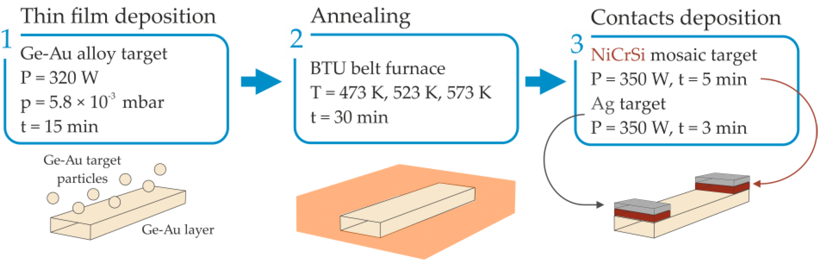
Thin films of germanium–gold alloy were fabricated by magnetron sputtering from circular alloy targets onto glass substrates (Corning 7059, Corning, NY, USA) using the Pfeiffer Classic 570 vacuum system (Wetzlar, Germany) with a WMK-100 magnetron. The gold content in the target was 5 wt.%. Investigated layers were fabricated in two processes: One with the addition of external bias voltage (
Ub = −150 V) to the glass substrate and the other one without external bias voltage. The tested thin films were fabricated under an Ar pressure of 5.8 × 10
−3 mbar and an applied constant power of 320 W. After the sputtering process, selected films were annealed at several temperatures: 473, 523 and 573 K using the six-zone BTU belt furnace (BTU International, North Billerica, MA, USA). To investigate the thermoelectric properties of germanium doped with gold layers, it was necessary to form the thermocouples containing thin films, so on the top of germanium-gold thin films, the two-layer NiCrSi/Ag contact pads were fabricated (also, using the magnetron sputtering under the constant power 350 W).
Figure 1 shows a diagram of the fabrication process of the Ge–Au/NiCrSi/Ag thermocouple.
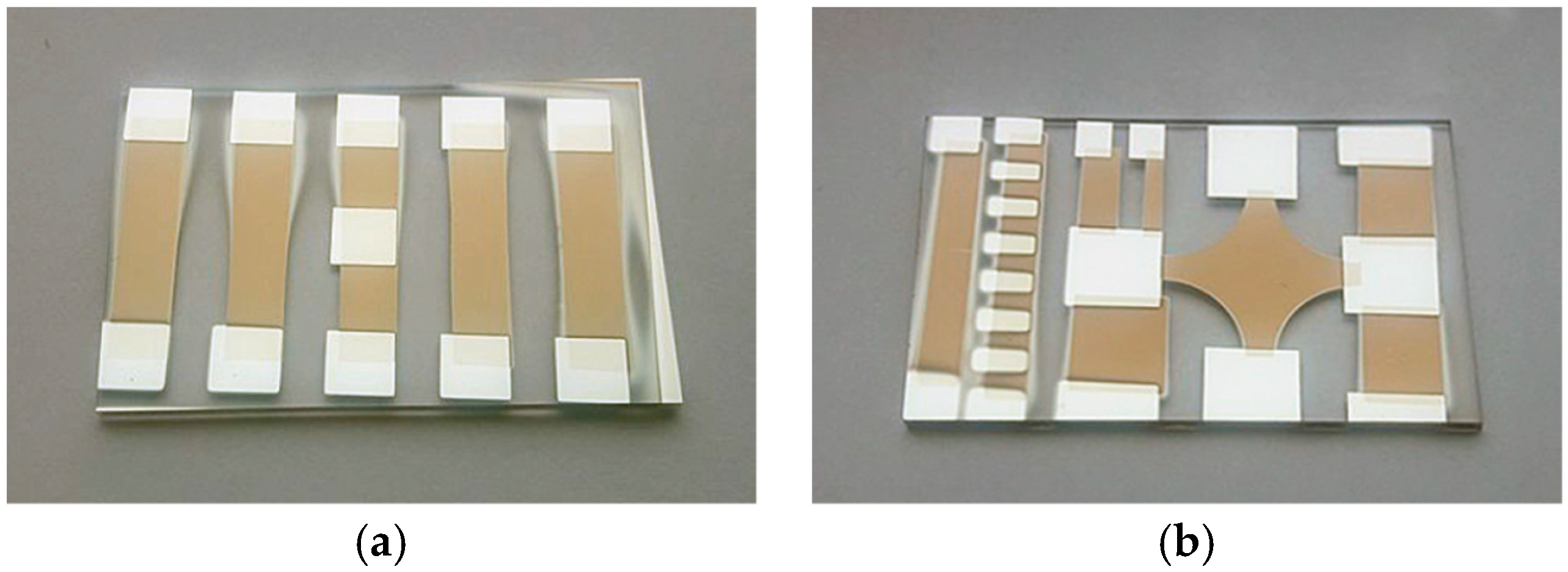
Figure 2 shows exemplary Ge–Au/NiCrSi/Ag test structures prepared for thermoelectric (
Figure 2a) and electric (
Figure 2b) measurements. As shown in
Figure 2a, in the case of structures for thermoelectric measurements, five separated structures were deposited onto one glass substrate, which was then divided into single test structures.
The Talysurf CCI optical profilometer was used to measure the thickness of deposited thin films and NiCrSi/Ag contacts. The average thickness of the Ge–Au films was 1.4 μm and the NiCrSi/Ag bilayer was 0.45 μm. The results obtained were used to calculate the resistivity and electrical conductivity of the layers as well as to determine the deposition rate as a ratio of film thickness to sputtering time. The average germanium thin films deposition rate was 1.5 nm/s.
3. Results
After the deposition and annealing process, four types of structures of germanium–gold thin films were obtained. In each group, there were three series of annealed thin films and one series of as-made layers. For all of the fabricated structures, the electric and thermoelectric properties were investigated. Additionally, in order to investigate the influence of deposition and post-process parameters on structural properties of films, the layers’ microstructure was studied.
3.1. Microstructure of Ge–Au Thin Films
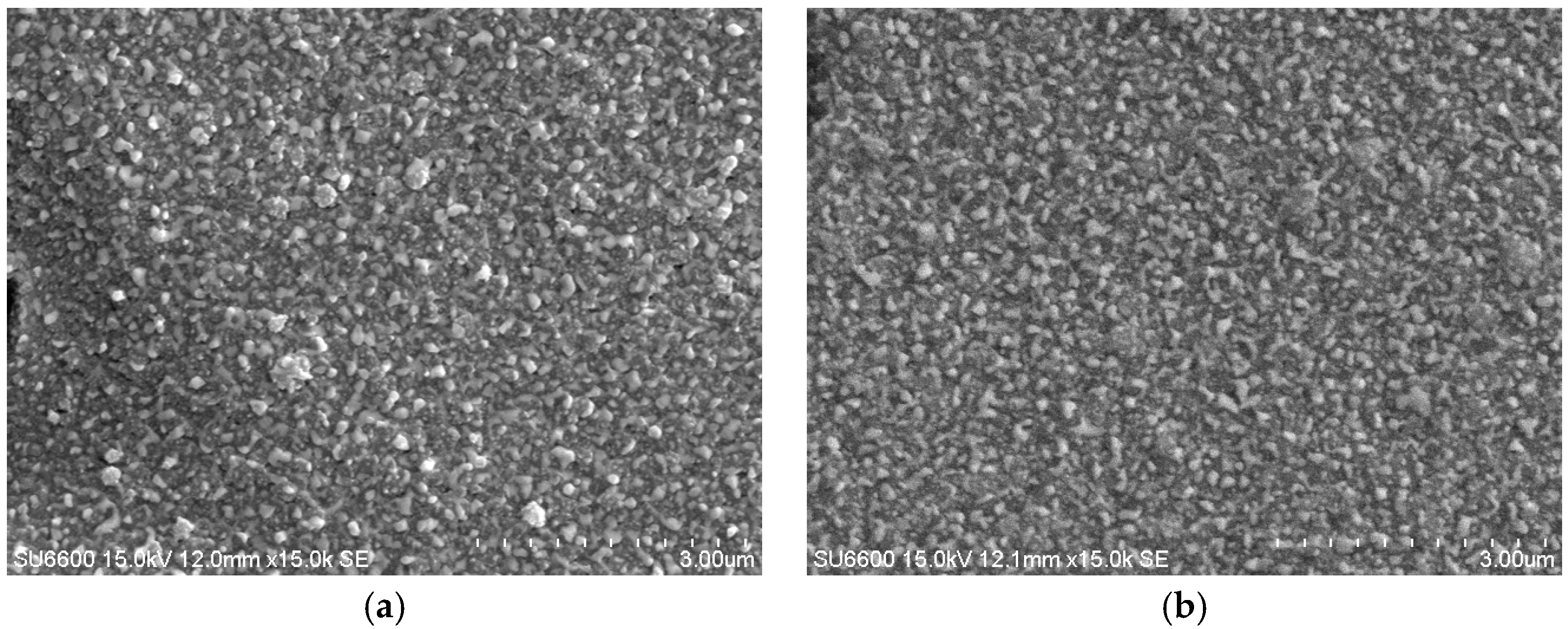
The structure of germanium–gold alloy thin films was investigated by scanning electron microscopy (Schottky Emission VP FE-SEM, SU6600, Hitachi, Tokyo, Japan).
Figure 3 shows SEM images of films fabricated under two conditions: as-made film sputtered without additional bias voltage (
Figure 3a) and film deposited with external bias voltage and then annealed at 573 K (
Figure 3b).
SEM images of the surface of both as-made and annealed Ge–Au thin films show that they are composed of visible, nanometer grains. In the case of as-made films deposited without external bias voltage (
Figure 3a), the size of grains was in the range from 60 to 300 nm with few grains bigger than 400 nm. For annealed films obtained in the sputtering process with additional bias voltage (
Figure 3b), grains were visibly smaller, and their size was in the range from 60 to 160 nm with few grains bigger than 200 nm. No cracks and defects on the surface were observed, which indicates the good quality of films.
Furthermore, the element composition of films was analyzed using the EDS detector (Thermo Scientific NORAN System 7, Madison, WI, USA). The microanalysis showed an average gold content in germanium films of 4.1% by weight and negligible amounts of carbon and oxygen atoms. Also, obtaining clear emission lines associated with the signal from germanium and gold indicates the high purity of thin films.
3.2. Electric Properties of Ge–Au/NiCrSi/Ag Test Structures
In terms of the electric parameters of thermoelectric materials, the most important one is electrical conductivity. In the presented work, the electrical conductivity was calculated using the van der Pauw method, based on measurements of films’ sheet resistance and resistivity. The described research were carried out at room temperature (approx. 300 K). In
Table 1, the resistivity and electrical conductivity are presented. For thin films fabricated in the process without any external bias voltage, the electrical conductivity at first increases slowly for annealing temperatures of 473 and 523 K, and then decreases for temperature of 573 K. On the other hand, for layers sputtered in the process with additional bias voltage, the following electrical conductivity values behavior was observed: at first, a drop of conductivity was observed (compared to unannealed films), and then the increase for annealing at 573 K.
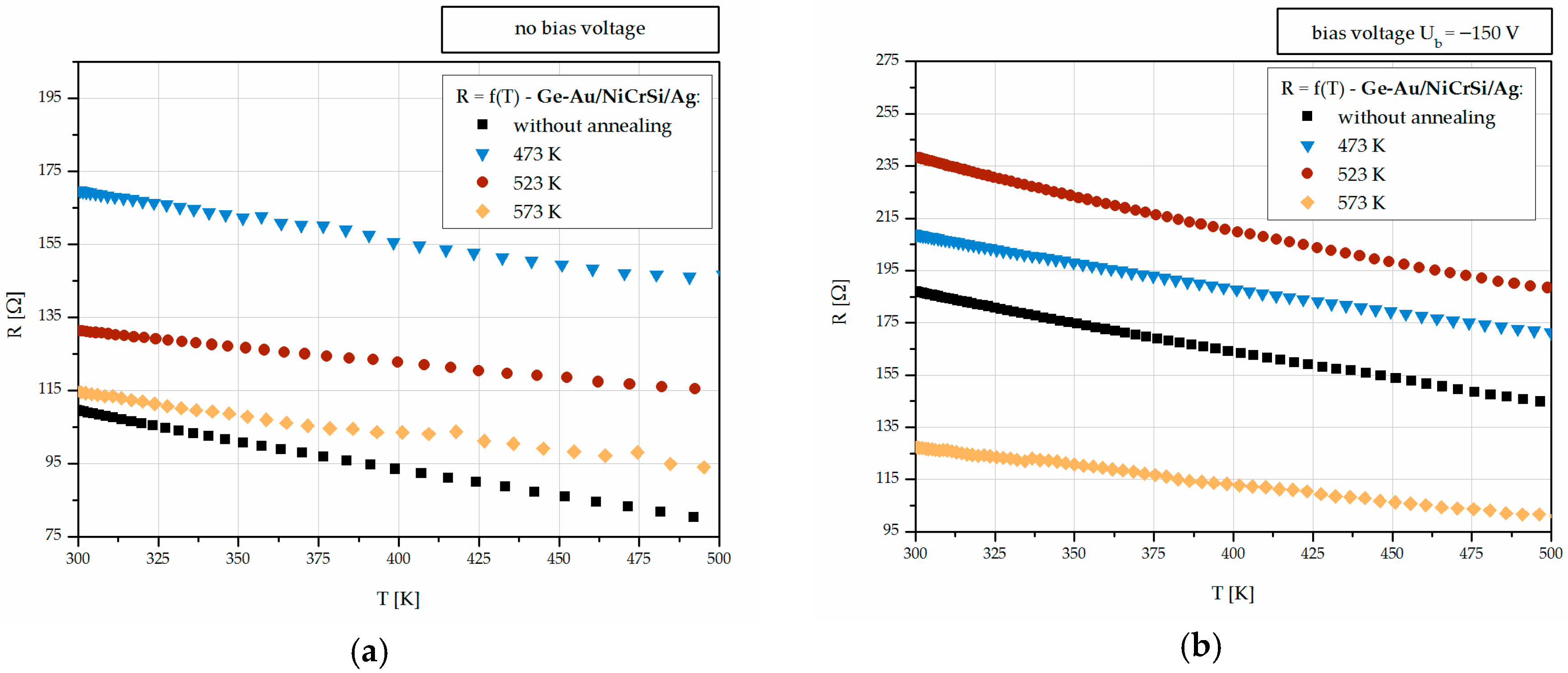
For further characterization of films, the temperature dependence of films’ resistance was measured (
Figure 4). For structures fabricated in the basic sputtering process (without additional bias voltage), it was observed that the resistance decreased within the annealing temperature; however, it was larger than for as-made structures. Additional bias voltage during the deposition of thin films resulted in an increase in the layers resistance and change in resistance behavior. In this case, the lowest resistance was obtained for film annealed at 523 K.
Based on the
R = f(
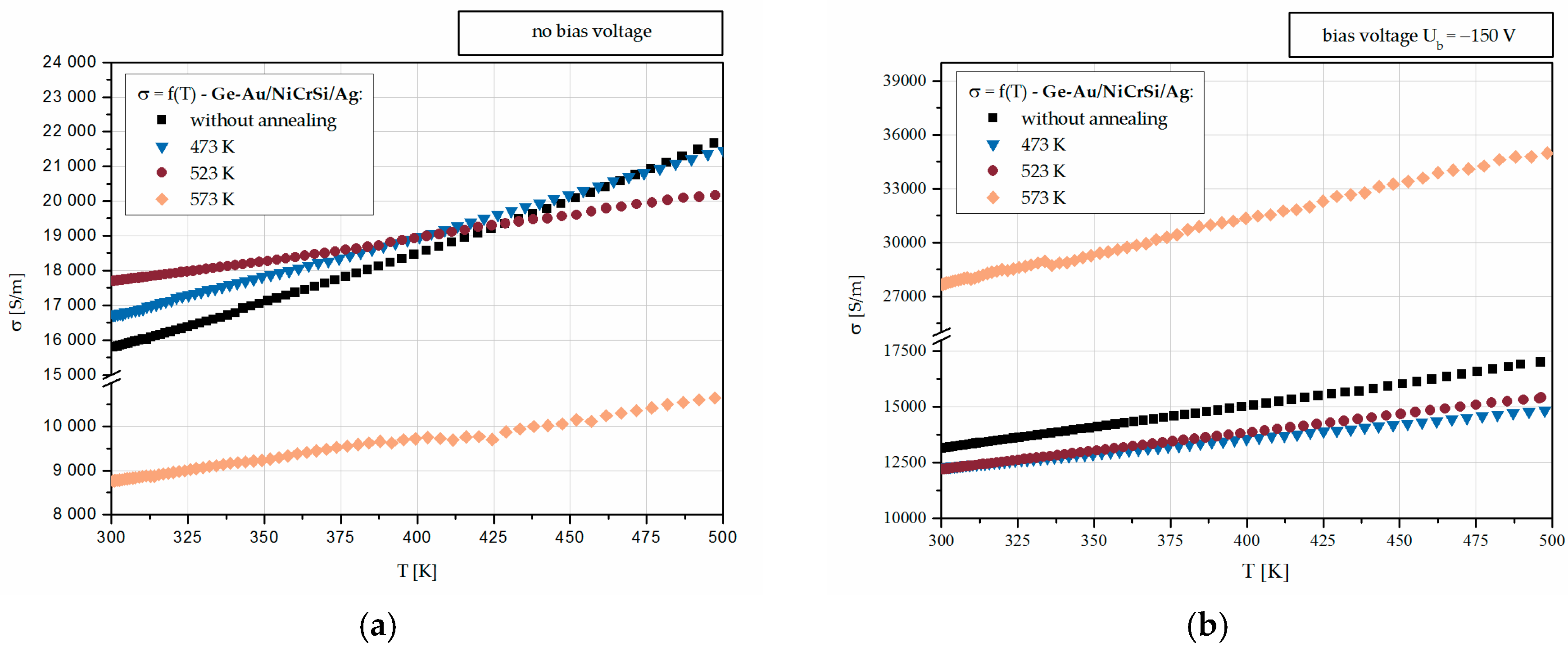
T) characteristics, the temperature-dependence of electrical conductivity was determined (
Figure 5). The electrical conductivity changed in a way typical for semiconductor materials—it increased within the temperature of the structure. The highest electrical conductivity was obtained for thin films sputtered in the process with additional bias voltage and then annealed at 573 K.
3.3. Thermoelectric Properties of Ge–Au/NiCrSi/Ag Test Structures
To characterize thermoelectric properties of germanium thin films doped with gold, the following parameters were determined: the thermoelectric voltage generated in the investigated thermocouples Ge–Au/NiCrSi/Ag, Seebeck coefficient of the material, power factor PF, and dimensionless figure of merit ZT.
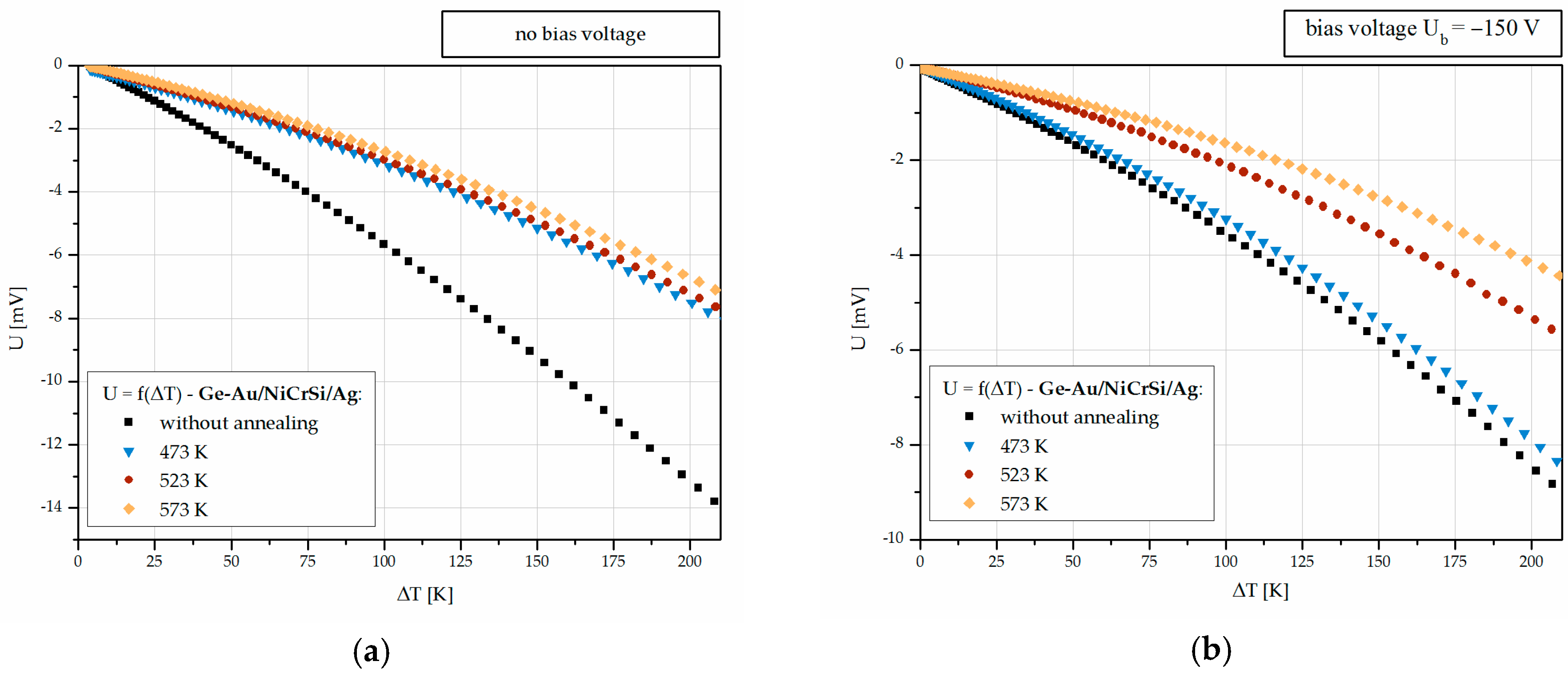
The thermoelectric voltage as a function of temperature difference between the hot and cold junctions of thermocouples was determined. The characterization of the thermoelectric voltage was carried out using the measurement setup in which the investigated test structure was placed on two separated plates, so that the thermocouple junctions (so-called hot and cold junctions) were positioned at two temperatures. In the presented measurements, the cold junction temperature was approximately constant (
T = 296 K) and the hot junction temperature increased from room temperature up to 490 K. Furthermore, two independent temperature sensors were used to directly measure the junctions’ temperatures. The thermoelectric voltage measurement results are shown in
Figure 6. As shown in
Figure 6a, for the thin films fabricated in the sputtering process without additional bias voltage, a significant drop in the values of the thermoelectric voltage generated in annealed thin films was observed. In the case of thermocouples with germanium layers sputtered with additional bias voltage, such a decrease was not as significant, but still, the highest thermoelectric voltage was generated in the as-made structures (
Figure 6b). All of the
U = f(Δ
T) curves had slightly increasing slopes, which indicates an increase in Seebeck coefficient within the temperature of the hot junction.
Based on the
U = f(Δ
T) curves, the Seebeck coefficient for each layer was determined using the integral method and Equation (3). The results are shown in
Figure 7.
where Δ
U is as thermoelectric voltage difference within temperature difference Δ
T.
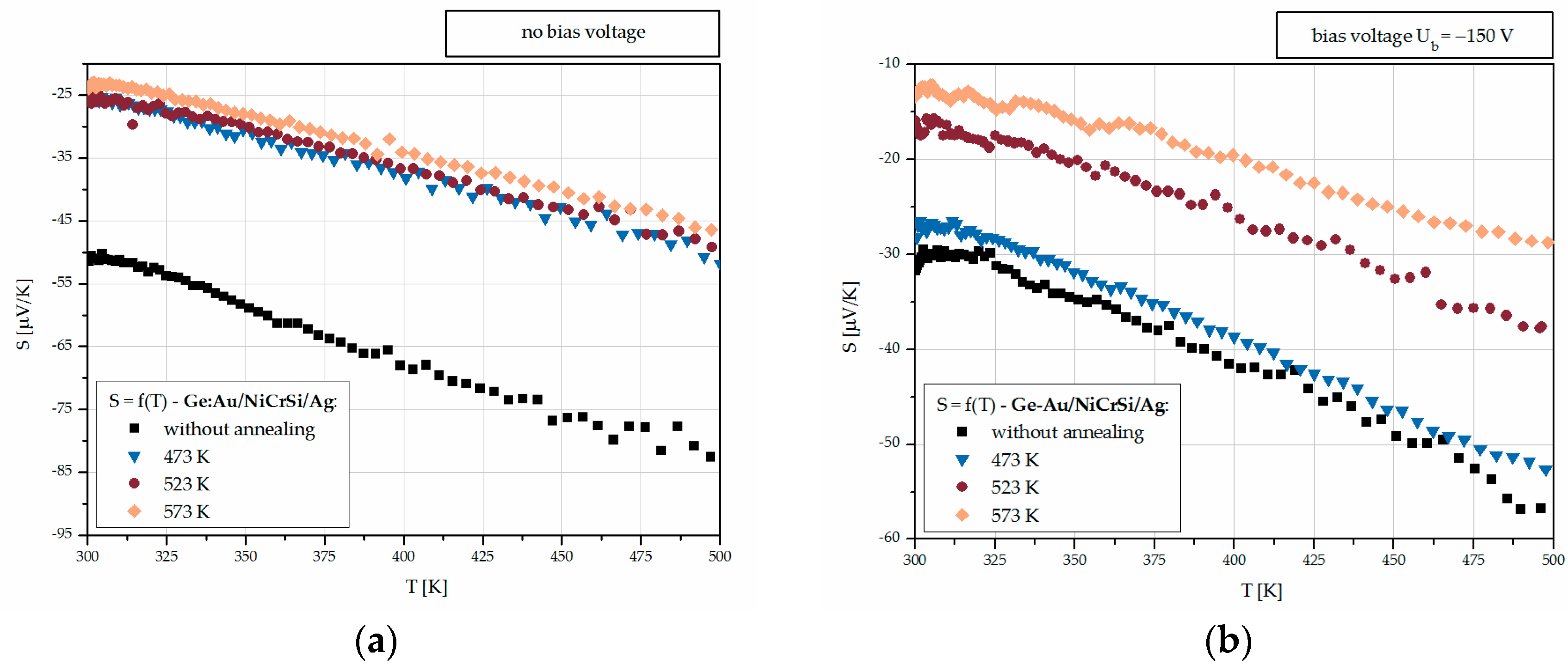
For all Ge–Au/NiCrSi/Ag structures, the Seebeck coefficient as a function of temperature exhibits a nonlinear, growing within temperature, character. For structures fabricated in the basic process (
Figure 7a), the significant drop in the Seebeck coefficient values of annealed thin films was observed (resulting from the thermoelectric voltage decrease). Also, the lowest values of the Seebeck coefficient of annealed films were calculated for structures sputtered with additional voltage (
Figure 7b).
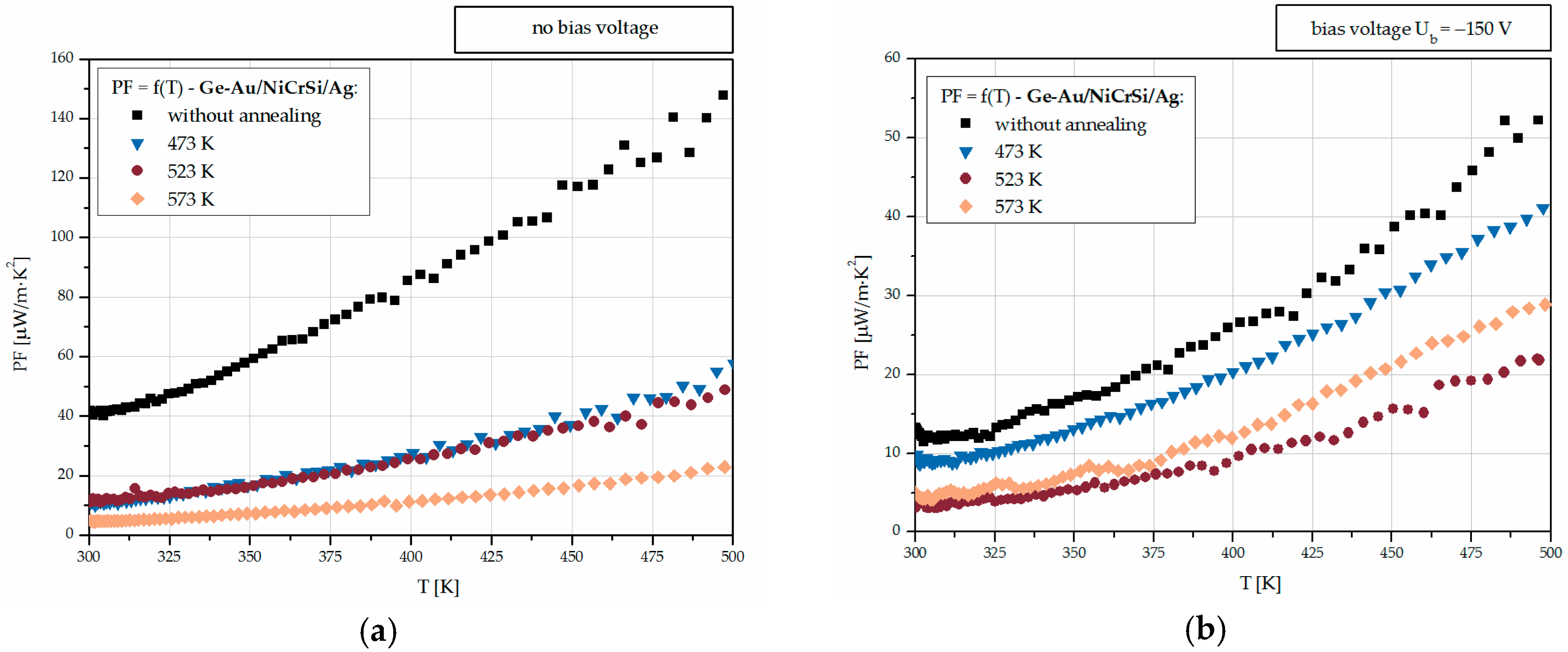
Based on the results of the Seebeck coefficient and electrical conductivity measurements, the power factor
PF was determined (using the Equation (1)).
Figure 8 shows the temperature dependence of
PF for the layers sputtered in a basis process (
Figure 8a) and in the process with additional bias voltage supplied to the substrate (
Figure 8b). In addition, the value of the dimensionless figure of merit was estimated.
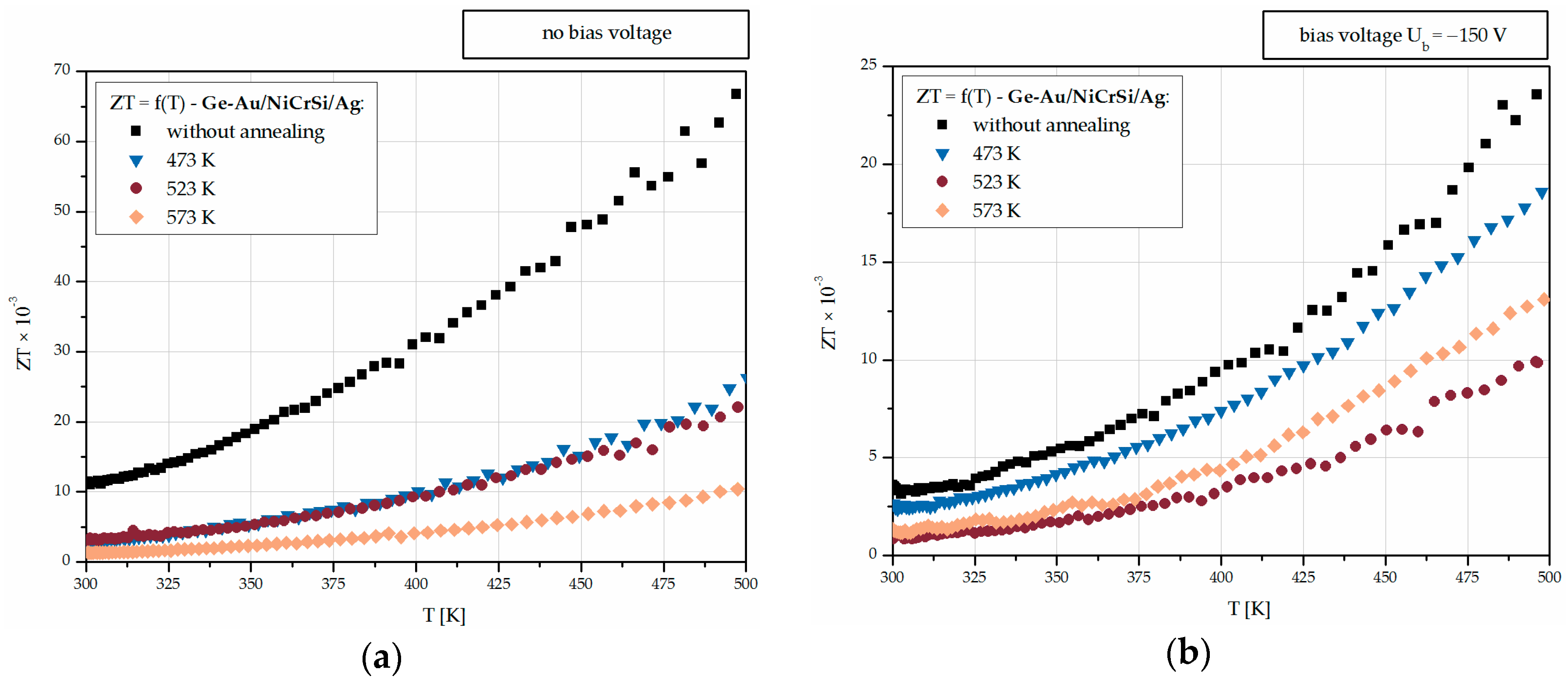
The dimensionless figure of merit
ZT and its temperature dependence was determined by the indirect method using the results of power factor measurements. In the described studies, the thermal conductivity value was assumed to be equal to 1.1 W/m·K. Such an assumption was made on the basis of the previous results presented in the literature describing thin film thermoelectric materials, as well as the studies in which the thermal conductivity of the substrate was assumed for the thermal conductivity of the layer [
32,
33,
34,
35]. In the presented studies, germanium-based thin films were sputtered onto glass substrates with a thermal conductivity of 1.1 W/m·K at 300 K. The results of
ZT measurements are shown in
Figure 9.
In
Table 2, the electric and thermoelectric properties of investigated thin films of germanium–gold alloy are presented (determined at 300 K).
4. Discussion
From the presented research, it is apparent that the deposition and post-processing processes parameters have a considerable influence on the electric and thermoelectric properties of thin film thermoelectric materials.
Undoubtedly, the electric and thermoelectric parameters of thin films result directly from their microstructure. The films’ microstructure in turn is related to the sputtering process and mobility of the adatoms during growth. The total energy supplied to the atoms and therefore the morphology and microstructure of thin film, depends on: the substrate temperature, final working pressure in the vacuum chamber, bias voltage applied to the substrate, and thermal characteristics of the target. In the presented research, the additional bias voltage applied to the substrate was used to improve the deposition process by enhancing the structural ordering of the film.
Fabricated thin films of germanium–gold alloy exhibited high electrical conductivity, which further increased after thermal post-processing (with the exception of thin films sputtered without additional bias voltage annealed at 573 K). It can be concluded that the thermal post-processing led to the activation of gold dopant. For structures fabricated in the process with additional bias voltage, the gradual dopant activation process was observed, which resulted in a progressive increase in electrical conductivity. For thin films sputtered without additional bias voltage, similar behavior of electrical conductivity was observed for annealing temperatures of 473 and 523 K.
Additional bias voltage led to supplying growing layers with more energy and therefore to influencing microstructures as well as their physical properties. Accordingly, such films can be annealed at higher temperatures, which will not cause degradation of the layers and deterioration of their parameters. However, higher annealing temperatures resulted in a decrease of the Seebeck coefficient which influenced the PF and ZT.
Taking into account the results presented in
Table 2, the optimal thermoelectric parameters at room temperature were obtained for the thin films fabricated in the process without additional bias voltage and post-annealed at 473 and 523 K. For this layer, the Seebeck coefficient reached −25 µV/K, and the power factor reached 11.0 µW/m∙K
2. At the same time, this layer showed high electrical conductivity (1.7 × 10
4 S/m and 1.8 × 10
4 S/m).
An interesting phenomenon was observed in the investigated Ge–Au/NiCrSi/Ag test structures. In the considered temperature range, the electrical conductivity of the germanium–gold alloy increased within the increasing temperature of the structure, which is typical for semiconductor materials. At the same time, the Seebeck coefficient also increased with the increase in temperature. Typically, in thermoelectric materials, the Seebeck coefficient increases in an inverse proportion to the electrical conductivity. The interrelation between the electrical conductivity and Seebeck coefficient can be seen from a relatively simple model of electron transport in metals and degenerated semiconductors. In such a model, the Seebeck coefficient is inversely proportional to the carrier concentration, which in turn affects in a proportional way the electrical conductivity. So, the higher the concentration of carriers, the higher the electrical conductivity, but the lower the Seebeck coefficient. However, in films with a thickness of the order of 1 micrometer and micro- and nanocrystalline microstructures, the variable range hopping (VRH) may be a dominant mechanism for d.c. charge transport [
36]. This conductivity mechanism, in turn, can lead to a simultaneous increase in electrical conductivity and the Seebeck coefficient.
Due to the simultaneous increase in electrical conductivity and the Seebeck coefficient, the power factor and dimensionless figure of merit increase within increasing temperature. For as-made structures fabricated in a process without additional bias voltage, the maximum PF reached 151.2 µW/m∙K2.
5. Conclusions
This paper presents research on thin films of germanium–gold alloy (Au content: 5 wt.%) obtained by magnetron sputtering using an alloy Ge–Au target. The electrical (resistivity, conductivity) and thermoelectric (thermoelectric voltage, the Seebeck coefficient, the PF, and ZT) properties of films were described.
The results showed that the right selection of deposition process parameters is crucial to the fabrication of thin films with the desired thermoelectric properties. It is necessary to select and control the sputtering gas pressure, target, substrate type, additional bias voltage applied to the substrate, and current-voltage parameters of the plasma discharge. Also, the results clearly exhibit that for the optimization of thermoelectric properties of alternative materials, there must be a compromise between the high values of the generated thermoelectric voltage and the sufficiently large values of electrical conductivity and the Seebeck coefficient.
In order to evaluate the examined Ge–Au/NiCrSi/Ag test structures in terms of practical applications, it is necessary to specify that some of the materials may be used in sensors, while others can be used to fabricate microgenerators. Thin films characterized by a high Seebeck coefficient can be used in sensors (for example in IoT networks), while those characterized by a high power factor can be successfully applied in microgenerators.
For this reason, investigated layers may be considered in further research on thin film thermoelectric materials from the point of view of applications in both sensor and generator systems. In addition, it is possible to study complex material compositions based on germanium and gold alloys and optimize them in order to obtain the best thermoelectric parameters.
Moreover, the subject of further studies of germanium–gold material composition can be the exact characterization of the conductivity mechanisms in Ge–Au films. The preliminary analyses carried out using impedance spectroscopy have initially confirmed the hopping conductivity in the investigated thin films.


