1. Introduction
Thermoelectric generator (TEG) devices are of interest in waste heat recovery and as primary heat-to-electricity sources. One promising material concept of interest to achieve high-energy conversion efficiency is a superlattice, where each leg in a module is composed of hundreds of nanometer-scaled thick crystalline bi-layers. In the current research, the term superlattice is not appropriate because we do not have full crystallinity in our thin films, and thus, we refer to them as multilayers. Even though the films are not fully crystalline, the defect doped behavior should be close to that of the crystalline material since the bands and electronic structure are similar to a crystalline material, and even purely amorphous material is capable of semiconductor behavior and quantum well effects [
1,
2,
3,
4,
5].
Theoretical work of Hicks and Dresselhaus showed that nano-scaled superlattices (SLs) would display a quantum well effect that increases the carrier effective mass, which increases the Seebeck coefficient while leaving the mobility unchanged and increases the electrical conductivity. This theory suggested that
zT values could be ~13-times higher than the bulk material values [
6]. In later work, Chen et al. [
7] and Ezzahri et al. [
8] both showed that the electrical conductivity increased, and the thermal conductivity decreased in a superlattice structure. Consequently, these studies show that all three properties of the figure of merit are affected such that the
zT is increased with a superlattice structure. In related and more recent work, Lee et al. [
9] showed the enhanced Seebeck coefficient for SrTiO
3/SrTi
0.8Nb
0.2O
3 superlattices, and Liu et al. [
10] showed the promising in-plane thermoelectric (TE) properties on Si/Ge SLs. These more recent studies show increases of the figure of merit by an order of magnitude over bulk material. In addition, recent data from superlattices of GaN/AlN/AlGaN grown by chemical vapor deposition at high temperature showed that enhanced
zT values could be obtained over bulk properties at room temperature [
11].
In further theoretical work, testing done by Ghamaty and Elsner [
12] and Balusu and Walker [
13] showed the decoupling of the Seebeck coefficient and the electrical conductivity due to the quantum well effect, which increases
zT [
14]. Early n-type Si/Si
0.8Ge
0.2 and p-type B
4C/B
9C superlattices were deposited using molecular beam epitaxy [
15] and magnetron sputtering [
16], but a potentially faster and less expensive method is ion beam sputtering since the ion energies and sputter yields are higher [
17]. Furthermore, excellent thermoelectric properties have been reported for Si/SiC, Si/Si
0.8Ge
0.2 and B
4C/B
9C superlattices using magnetron sputtering. A module
zT near 4 at 523 K was reported for these materials [
18,
19,
20], and more recent data for Si/SiC superlattices on silicon substrates made by magnetron sputtering [
21] and ion beam sputtering [
22] indicate even higher
zT in high temperature applications. For the above studies, there is a significant doubt about the performance data due to the poor reproducibility with the resistivity measurements done with Si/SiC on silicon substrates as originally demonstrated [
21].
In the current research, insulating substrates are used to get a true measure of the electrical properties, and the lattice thermal conductivity of the ML film was measured using the MEMS technique performed at the University of Denver where our ML was deposited on Si, and the Si thermal conductivity was subsequently measured to subtract from the total thermal conductivity yielding a measure of only the ML [
22]. Several studies have shown that superlattices with a layer thickness of 5 to 10 nm have thermal conductivity of less than 5 W/mK. Some of them are the studies done by Aubain et al. [
23] on the lattice thermal conductivity and the study done by Mazumder et al. [
24] on the total thermal conductivity at different temperatures, specifically for Si/SiC films. These thermal conductivity measurements include the 3-ω transient method and the thermal reflectivity method, which are both well-accepted techniques.
2. Materials and Methods
Before installing the silicon and the quartz substrates in the vacuum system, they were cleaned and rinsed with acetone, isopropyl alcohol and deionized water and dried. For the mullite (3Al
2O
3·2SiO
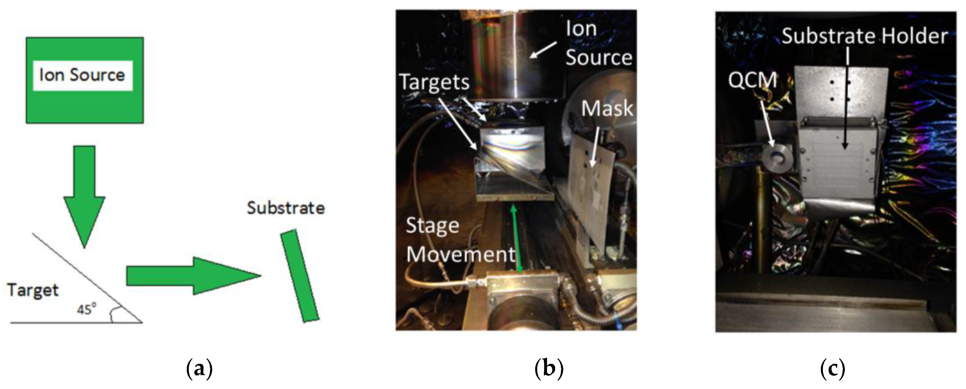
2) substrates, no pre-cleaning preparation was performed. The configuration of the sputter deposition process is shown in
Figure 1. Sintered Si and SiC sputter targets were used. Inside the chamber evacuated to 3 × 10
−6 Torr, a stage moved targets under a stationary ion beam to sputter different materials onto the substrates. The targets were mounted at forty-five degrees relative to the ion beam and the substrate holder as shown in
Figure 1. A second stage was used to position a mask over the substrate to control layer thickness. During deposition, the temperature of the substrates was held constant at about 773 K, and the partial pressure from Ar from the ion beam source is 5 × 10
−3 Torr. The deposition rate is slowed to 3 nm/min by lowering the ion beam energy to 300 eV during the first 1.0 nanometers of growth of each layer to ensure sharp interfaces and less mixing at the interfaces. The remainder of each ML layer is grown more quickly at 10 nm/min using 1000 eV ions. A total of 31 bi-layers of silicon and silicon carbide were deposited to form multilayers structures. Each layer consists of 10 nm of Si followed by 10 nm of SiC.
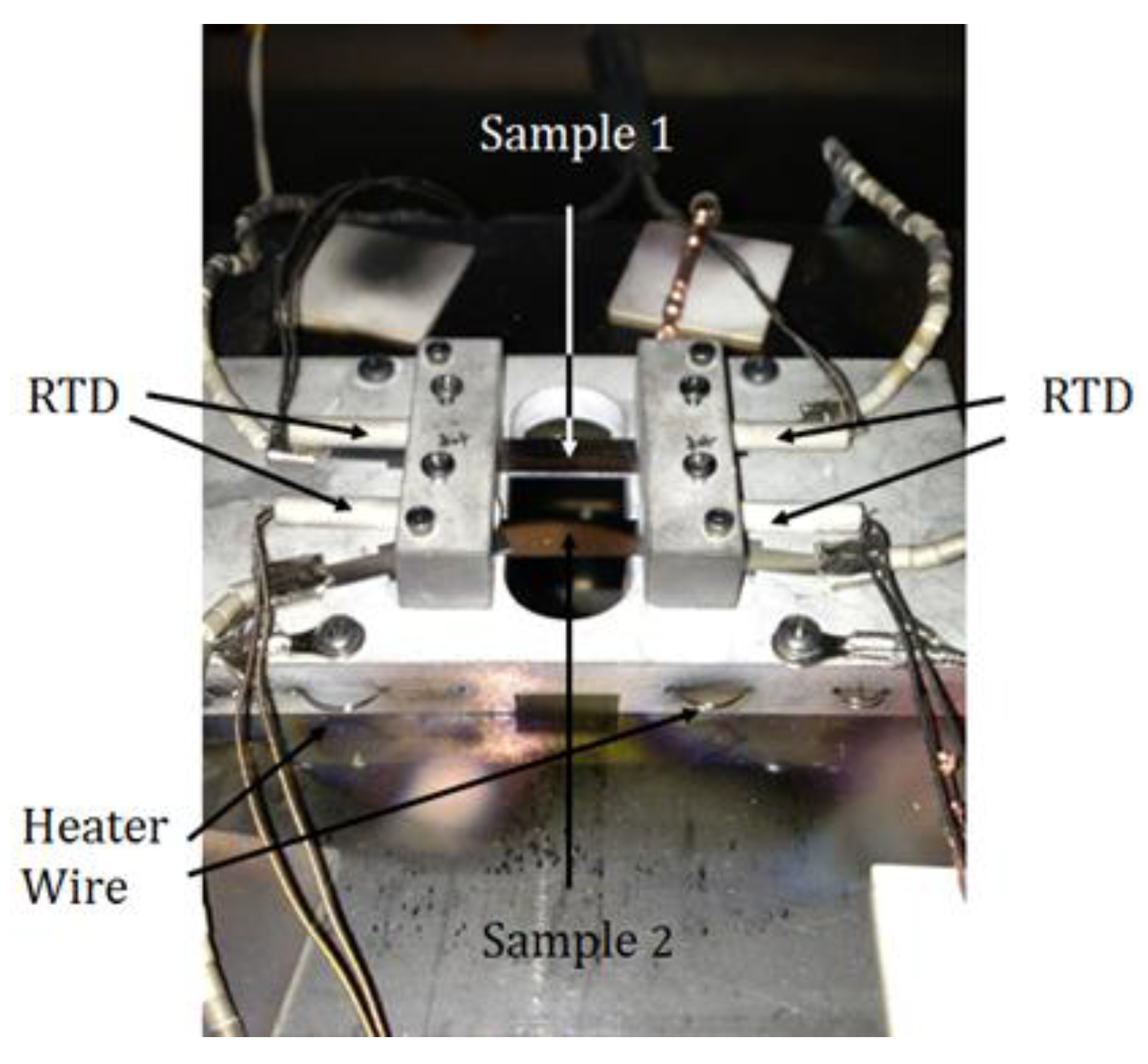
After the ML films are deposited onto the substrates, they are installed into a separate vacuum test facility where the Seebeck coefficient and the electrical resistivity were measured over a temperature range from 300 K to 900 K. The Seebeck coefficient is measured in plane by heating up one side and keeping the other side within 20 degrees of the hot side while measuring the voltage across the samples and the temperature across the sample. The resistivity is measured in plane as well by measuring the electrical resistance and knowing the geometry. A photograph of the test setup is shown in
Figure 2. Two substrates can be mounted onto the sample holder and tested at the same time. The substrate holder is made of boron nitride. The tungsten wire-based heater was used to control the temperature of each side such that a small temperature difference is established across the substrate. The maximum possible achievable mean temperature was 870 K. Resistance temperature detectors (RTDs) (Omega Engineering Inc., Norwalk, CA, USA) were used rather than thermocouples for measuring temperatures. SEM of the MLs was done with a JEOL-JSM 6500F (JEOL Ltd., Tokyo, Japan) in secondary electron mode. TEM of the MLs was done with a JEOL JEM-2100F (JEOL Ltd., Tokyo, Japan) with the ultra-high resolution (UHR) objective pole piece and EDS from Oxford Instruments Max 80 SDD (Oxfordshire, UK). The crystal structure of the deposited MLs on the silicon substrate was analyzed using XRD with a Bruker D8 Discover (Billerica, MA, US) with a Cu (Kα) source scanning at 1 s per step with a step size of 0.02°. The energy of the beam was 40 keV at 40 mA. The mobility of the ML films was measured using the four-point Ecopia HMS-3000 Hall measurement system (Bridge Technology, Chandler Heights, AZ, USA).
3. Results
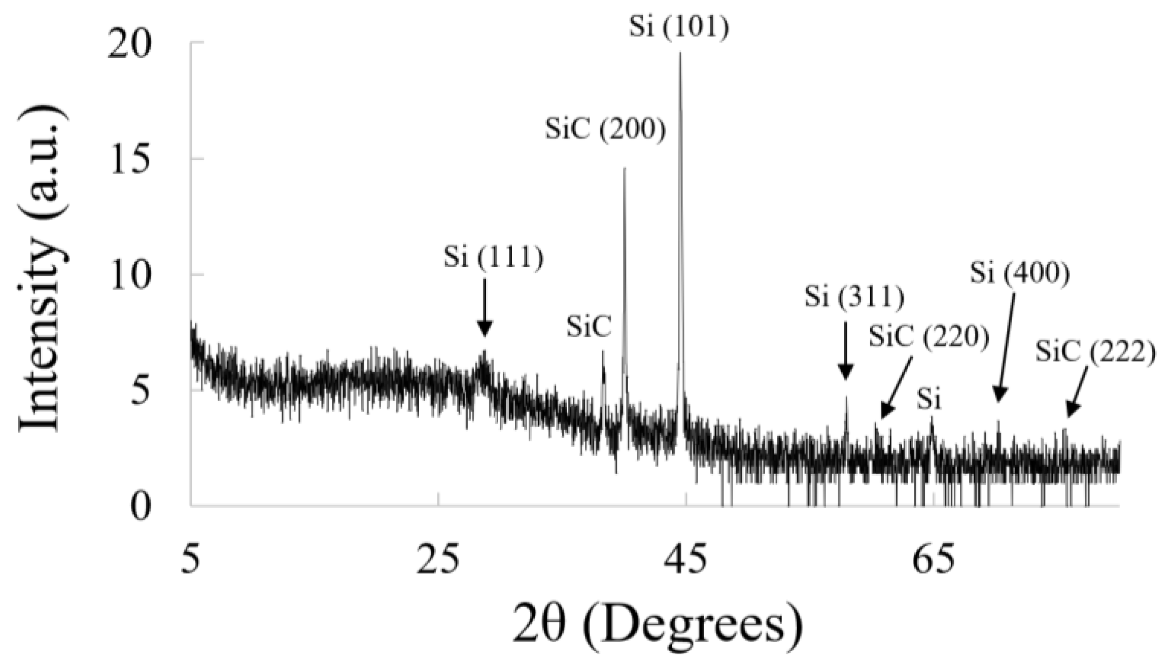
The crystal structure of the thin films on silicon was investigated with XRD where all peaks are identified with respective planes except for two.
Figure 3 shows some small crystalline peaks at 37, 40, 60 and 76 degrees from SiC. The peaks around 27, 45, 57, 65 and 70 degrees are from Si. The recorded silicon peak at 27 degrees is similar to the one found by Surana et al. [
25]. The recorded silicon peak at 65 degrees was identified from Yang et al. [
26]. In general, the films show some crystallinity with the Si (101) peak coming from the substrate, and later, TEM further shows the distributions revealing that the films have some pockets of grains among otherwise amorphous material. The small peaks are likely from small amount of Si and SiC that are crystalline, as will be shown in TEM later. The broader peaks at 27, 57 and 65 degrees are amorphous peaks, which is the reason to believe that the films are not entirely polycrystalline, but have some areas of grains and some areas of amorphous material for both materials in the ML.
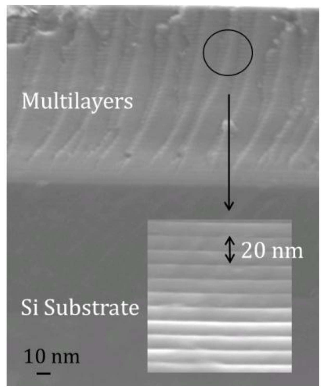
Figure 4 shows a cross-section of the ML thin film that was investigated using scanning electron microscopy (SEM). The cross-section of the ML thin film on the silicon and the quartz was used for the SEM and the TEM analysis. In both cases, the films were deposited at 773 K and tested in the thermoelectric property measurement system from 323 K to 903 K. The SEM image of the multilayer thin film structure on the silicon substrate shown in
Figure 4 is used to measure and verify the ML structure, layer thickness and uniformity of the thin film; however, it is difficult to tell how much intermixing is occurring at the interfaces between the layers and difficult to get good data for the Si/C ratio for the SiC layer.
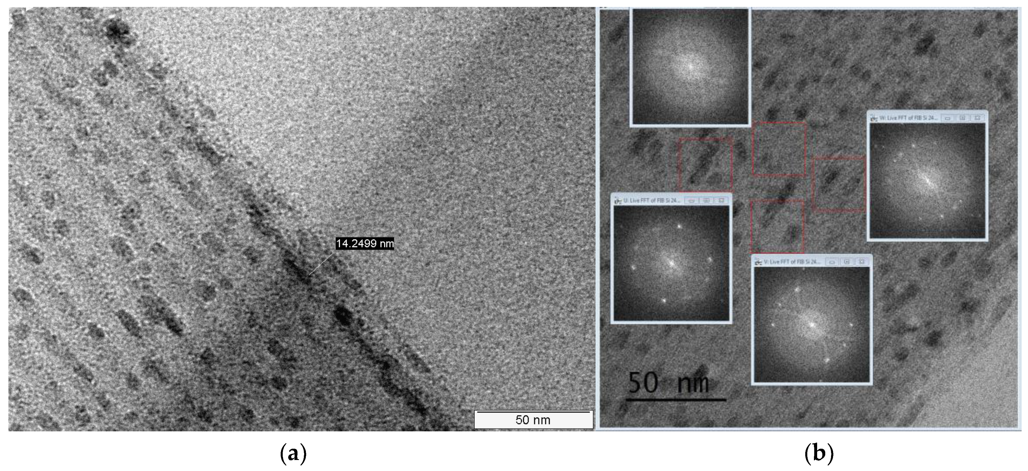
Figure 5 shows a transmission electron microscopy (TEM) image of the substrate and ML that was milled out with a focused ion beam (FIB). The substrate used for this ML thin film was quartz. The substrate and film can be distinguished, and the ML film layer size is shown.
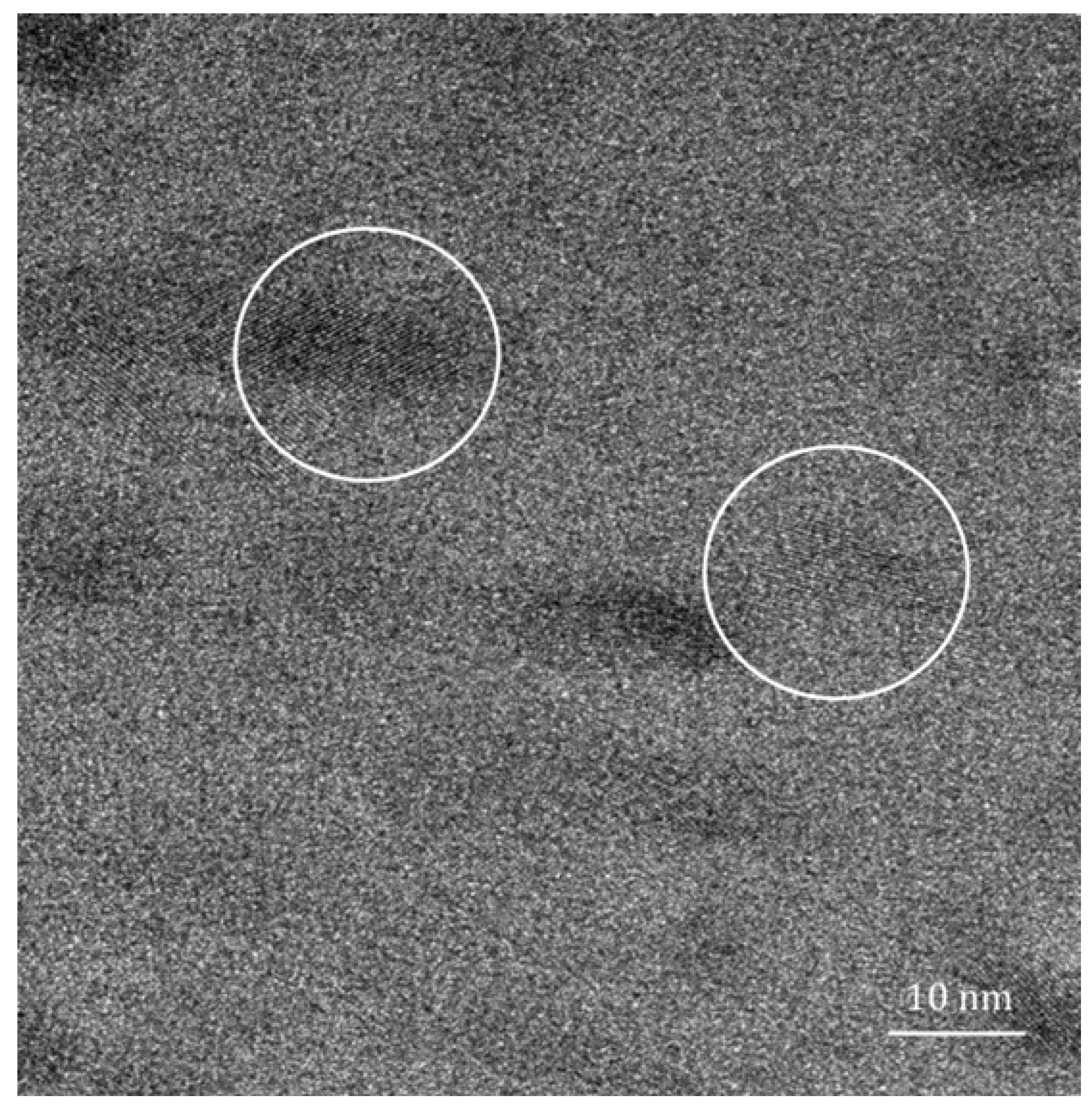
Figure 6 shows that the film has pockets of different material behavior. The fast Fourier transforms (FFTs) show that the pockets in the ML films mostly crystalline and are likely grains. The materials mapping data from EDX with the TEM measurements were inconclusive likely due to the FIB mixing of the materials. The crystallinity is most likely more from the Si than from the SiC because deposition is done closer to the recrystallization temperature of Si and not SiC. There is still some crystallinity in the SiC layer as the (200) plane shows up very well.
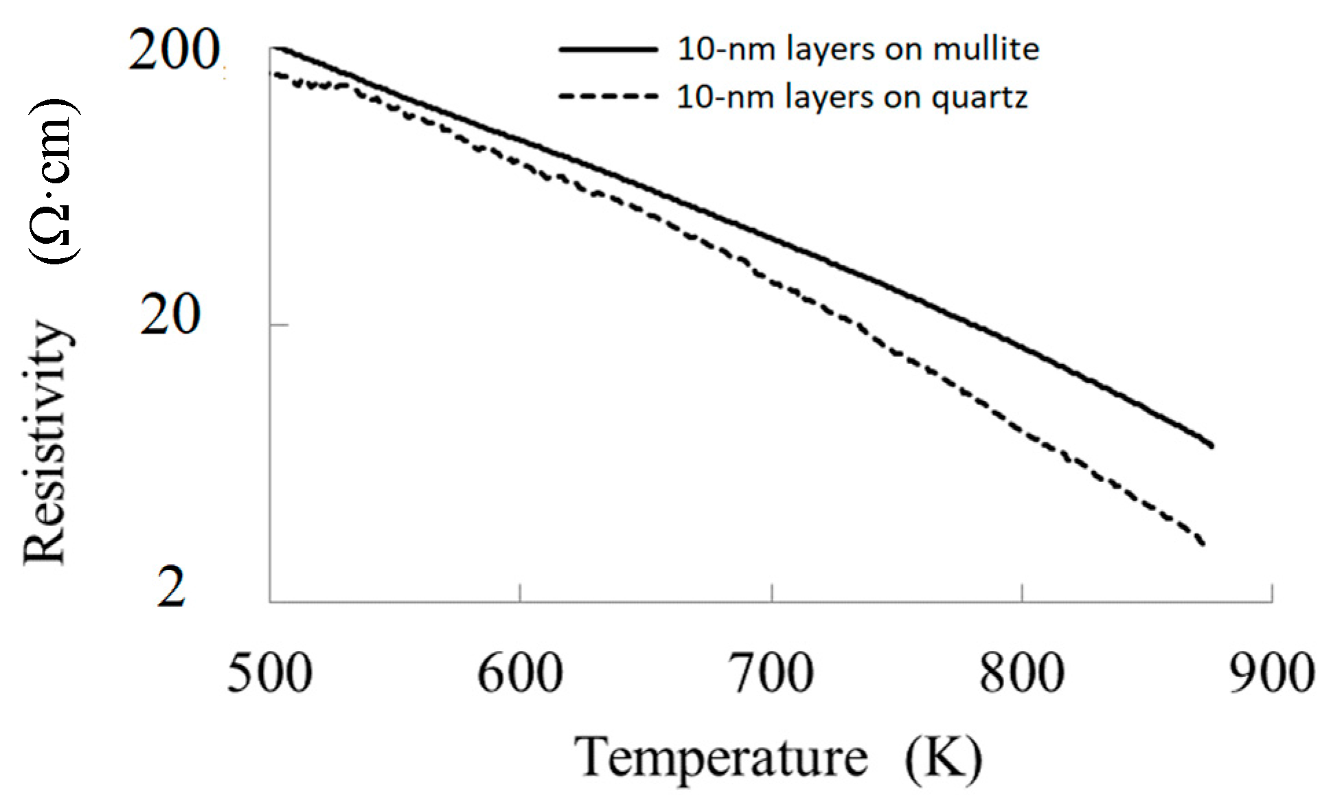
Figure 7 shows the plot of resistivity versus temperature for MLs on quartz and mullite. In the current research, quartz and mullite substrates are used for the ML thermoelectric measurements since the Si substrate interferes with the measurements. The MLs on the quartz and mullite substrates show similar resistivities; however, the resistivity of the thin film on the quartz is lower compared to the mullite substrate. Since quartz and mullite are both insulators, the decrease in resistivity on the quartz substrate may be from the quality of film and interfaces made. The resistivity data gathered in this study are significantly higher than data previously shown in the literature on the silicon substrate, likely due to the conductivity of the silicon substrate, but follow the same semiconductor trend for the temperature range tested [
19,
21,
22].
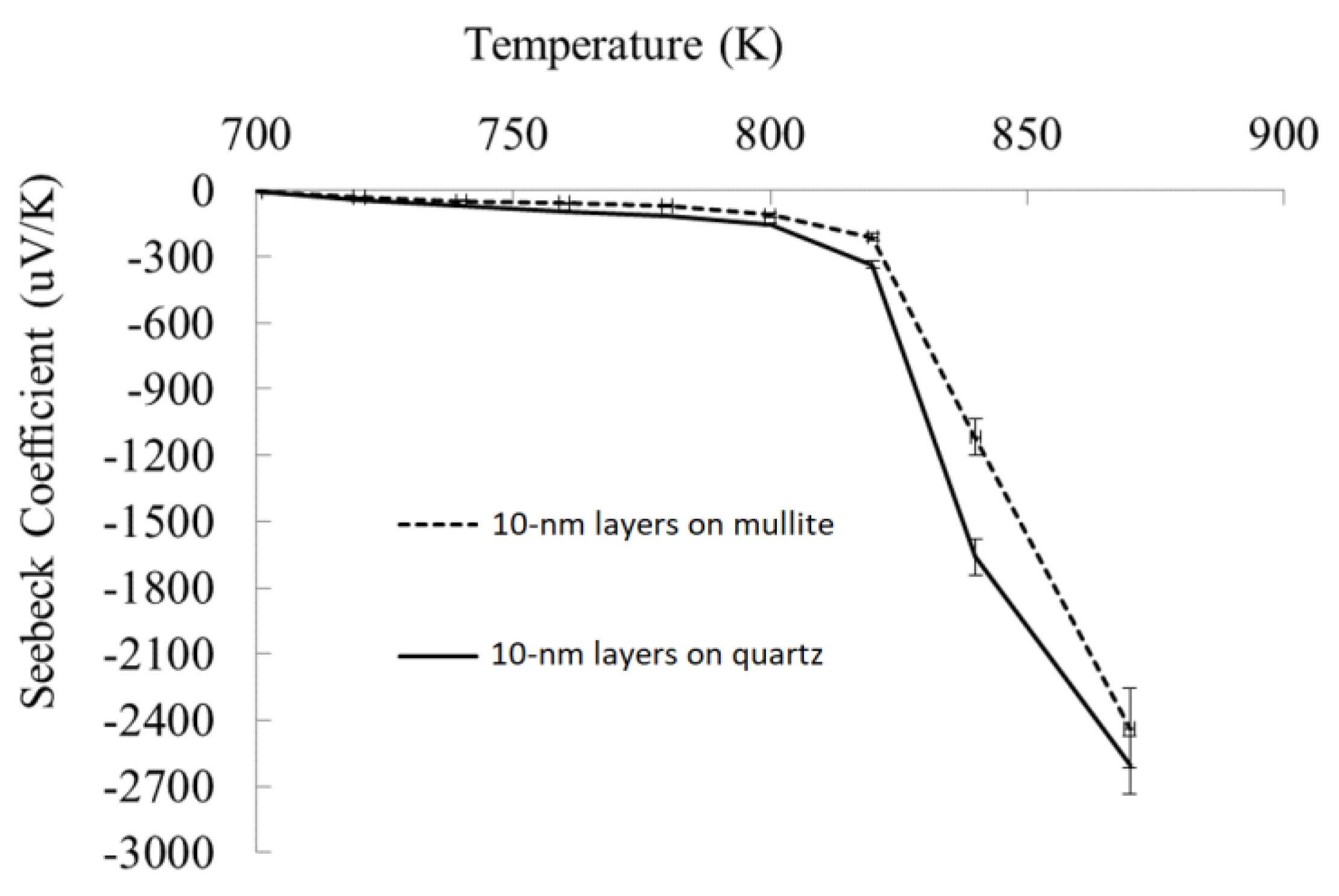
Figure 8 shows the Seebeck coefficient measurements of the ML thin films on quartz and mullite. The multilayer thin films on the quartz and the mullite samples have very low Seebeck coefficient values until the temperature reaches the value of 800 K. The multilayer thin films reach a stunningly high Seebeck coefficient, producing over 100 mV. The films are n-type as the two multilayer materials are intrinsically n-type. The giant Seebeck coefficient values of the ML thin films on the quartz and the mullite were repeatable and were observed at the multiple temperature ramps on the multiple thin film samples.
Table 1 shows that the Seebeck coefficient decreases by 5.8% and 6.5% on the MLs on the quartz and the mullite substrates, respectively, after 3 cycles. The metal contacts started to delaminate slightly from the ML thin films on the quartz substrate after just one cycle. The best thermoelectric properties were obtained from the ML thin film on the quartz substrate, but the ML thin film had some cracks near the metal contact after one thermal cycle due to the mismatch in thermal expansion coefficient between the quartz substrate, metal contact and ML thin film. However, data are still collected for this sample for two more cycles, so the mechanical cracking is not enough to compromise the whole film for studies. Ideal contacts for this system could not be obtained [
27]. This is an issue if these MLs are to be used in a module.
Finally, the mobility of the ML thin films was measured at room temperature using a the 4-point probe Hall mobility system to separate the carrier density component of the electrical conductivity. The mobility is low and looks very different for the multilayer thin films on the two substrates. It is also noted that the room temperature carrier concentration is low for the multilayer thin films on the two substrates. Lower values of the mobility and the carrier density are indicative of amorphous materials.
Table 2 shows the mobility and carrier concentration of the films on quartz and mullite substrates. The expected mobility of amorphous silicon and the silicon carbide is in the range of 0.1 to 10 cm
2/Vs [
28,
29]. The mobility values of the multilayer thin films in this study are in this range. This verifies that the multilayer thin films in this study have some amorphous nature.
4. Discussion
A limited number of TE property measurement tests were repeated three times to determine the reproducibility of the thermoelectric measurements. The experiments show good repeatability for the Seebeck coefficient from ML thin films deposited on the mullite substrates where the ML thin films, and the metal contacts did not crack.
One interesting phenomenon in our ML thin films is the appearance of the high Seebeck coefficient effect at higher temperature on the quartz and the mullite substrates. The turning on of the giant Seebeck coefficient is not well understood, but it is hypothesized that it is a strain-induced effect due to the mismatch of the interfaces since the electrical resistivity behaves as a regular semiconductor would. The strain-induced Seebeck coefficient seen at higher temperatures has been suggested and modeled in several studies with the band convergence and the enhanced effective mass [
30,
31,
32,
33]. The layers with some limited crystallinity likely line up better and allow the emergence of phenomena at the interfaces when the thin film samples are given enough thermal energy to reduce the strain in the films. This is a possible mechanism because the thermal expansions of the two multilayer materials is different enough to cause interface shifting at higher temperatures, and the carriers in one material could activate and transport in the other at higher temperatures.
Our testing apparatus could not be used to drive the temperature above ~900 K, and thus, there are no data available above 900 K. In addition, as discussed before, our metal contacts began to degrade when they were tested to 900 K, but unlike the Seebeck coefficient, the resistivity had significantly increased after each test likely due to cracking of the metal contacts and annealing. That is why we need both the better electrical contacts and the higher temperature measuring system to further study the emergent phenomena that have been observed. The existence of Giant Seebeck in this system is very significant because the Seebeck is almost 4 times higher than a normal Si system, which means the zT would be a factor of 16 better if the resistivity was lower.
Table 3 shows the figure of merit,
zT, values for 10-nm layers of Si/SiC ML structure. There is an observed tradeoff in the thermoelectric properties that yielded a relatively low figure of merit,
zT, where
zT =α
2T/ρ; α is the Seebeck coefficient, which is a measure of the amount of voltage per degree temperature difference;
is the temperature; ρ is the electrical resistivity, and 𝑘 is the thermal conductivity. If the MLs possessed better resistivity with a simultaneous increase in Seebeck coefficient, then the MLs figure of merit would be increased significantly and surpass many known materials.
The higher Seebeck coefficients at high temperature suggest that the giant Seebeck coefficient effect has been observed in the Si/SiC ML thin film system. This is a very high Seebeck coefficient for films made with ion beam deposition. The giant Seebeck coefficient is a term reserved for systems enhancing the Seebeck coefficient beyond the bulk values with the quantum confinement. Most of the studies reporting giant Seebeck coefficient were observed in the systems utilizing oxides and precise doping. Ohta et al. [
34] and Lee et al. [
9] have both observed the giant Seebeck coefficient in SrTiO
3 systems with values near −1000 μV/K, and Song et al. [
35] have observed the giant Seebeck coefficient for MnO
2. More recently, the giant Seebeck coefficient seen in the silicon nanoparticles is in the range of our ML thin films [
36]. The most recent giant Seebeck system is the SnSe system with ~1000 μV/K [
37]. These studies provide additional evidence that Hicks and Dresselhaus’s [
6] theoretical work is of current significance.
Full decoupling of the carrier concentration and Seebeck coefficient may never be achieved, but the recent evidence shows that the giant Seebeck coefficient could be produced in a high temperature material that has some amorphous nature. Systems designed for a high Seebeck coefficient like superlattices and multilayers have the potential for performing carrier concentration tuning, thus shifting the maximum of the
zT versus carrier density plot to the left and upward for a higher, more efficient material with relatively lower carrier concentration, which is the reverse of the approach followed recently by the materials science community in skutterudites, clathrates and chalcogenides [
38]. The turning on of the giant Seebeck coefficient does not happen until high temperature, where carriers are activated. Once carriers are activated in the ML, then they can transport. The giant Seebeck is then observed because of the layered structure and enhanced density of states. This gives more energy per electron, which increases the Seebeck coefficient. The resistivity is not affected significantly from our data because the resistivity is not enhanced and acts like a regular semiconductor, and the level of crystallinity in our films allows for the quantum confinement to enhance the Seebeck coefficient.
5. Conclusions
The ion-beam-based deposition system was configured to grow Si/SiC multilayer thin films on mullite and quartz substrates. Typical ML thin films consisted of 31 bi-layers of a 10-nm layer thickness. The ML thin films were found to be have some amorphous nature with some regions of crystallinity. An impressive Seebeck coefficient of ~2600 μV/K was measured at this temperature along with a higher, less than desired, electrical resistivity of 3.4 Ω·cm. zT of 0.08 was calculated when these values were combined with a previously measured thermal conductivity of 2 W/mK. We have measured the highest Seebeck coefficient to date with Si/SiC multilayers on insulating substrates with values greater than −2000 μV/K. We showed evidence that there are enhancements in the Seebeck coefficient to the quantum confinement. Quantum confinement can enhance the Seebeck coefficient because of an enhanced density of states and effective mass, which increases the energy per electron, but this does not happen until electrons have promoted the conduction band, so that is why the giant Seebeck coefficient is not seen until high temperatures. With superlattices or multilayers made of semiconductor materials, the electrical conductivity is poor compared to traditional bulk TE materials that are in the semi-metal materials class. It is believed that the density of states of the effective mass was increased in our ML thin films on the mullite and the quartz substrates, which resulted in an increase of the Seebeck coefficient at higher temperatures. The turning on of the giant Seebeck coefficient at high temperature is not completely understood, but it is thought to be due to a strain-related effect.

 ,
, 


