1. Introduction
In grid-connected photovoltaic (PV) systems, modules are typically connected in series to build up a sufficiently high voltage output. To minimize ohmic losses, PV power plants are increasingly operated at high system voltages. At the end of a string, modules can have nominal system voltages of ±1500 V relative to the ground. Although glass and other encapsulants, which are usually polymeric dielectrics, are electrical insulators, a small leakage current can be measured if a voltage is applied between cells and the frame. There are several possible current paths that can lead to many forms of potential induced degradation (PID) [
1]. Cu(In,Ga)Se
2 (CIGS) modules are reported to suffer in special configurations from negative polarization [
2,
3].
A defensive approach relies on grounding the negative pole at the inverter entrance. The problem, however, remains when transformerless inverters are used, which are quite common, as these are known to offer an absolute efficiency increase of around 2% compared to inverters with transformers [
4]. In this case, electric safety issues impede pole grounding. The result is a floating potential at the positive and negative DC poles.
In this paper, we report that a modification of the Mo back contact can lead to cells that are much more stable against high voltages, demonstrating highly increased stability against PID. The stability of such cells would, therefore, be independent from system and module techniques. The effects of high voltages on PID-susceptible CIGS cells and CIGS cells with increased PID stability are studied by capacitance–voltage (CV) and electron-beam-induced current (EBIC), glow discharge optical emission spectroscopy (GDOES), current–voltage (I–V), and energy-dispersive X-ray spectroscopy (EDX) measurements.
2. Materials and Methods
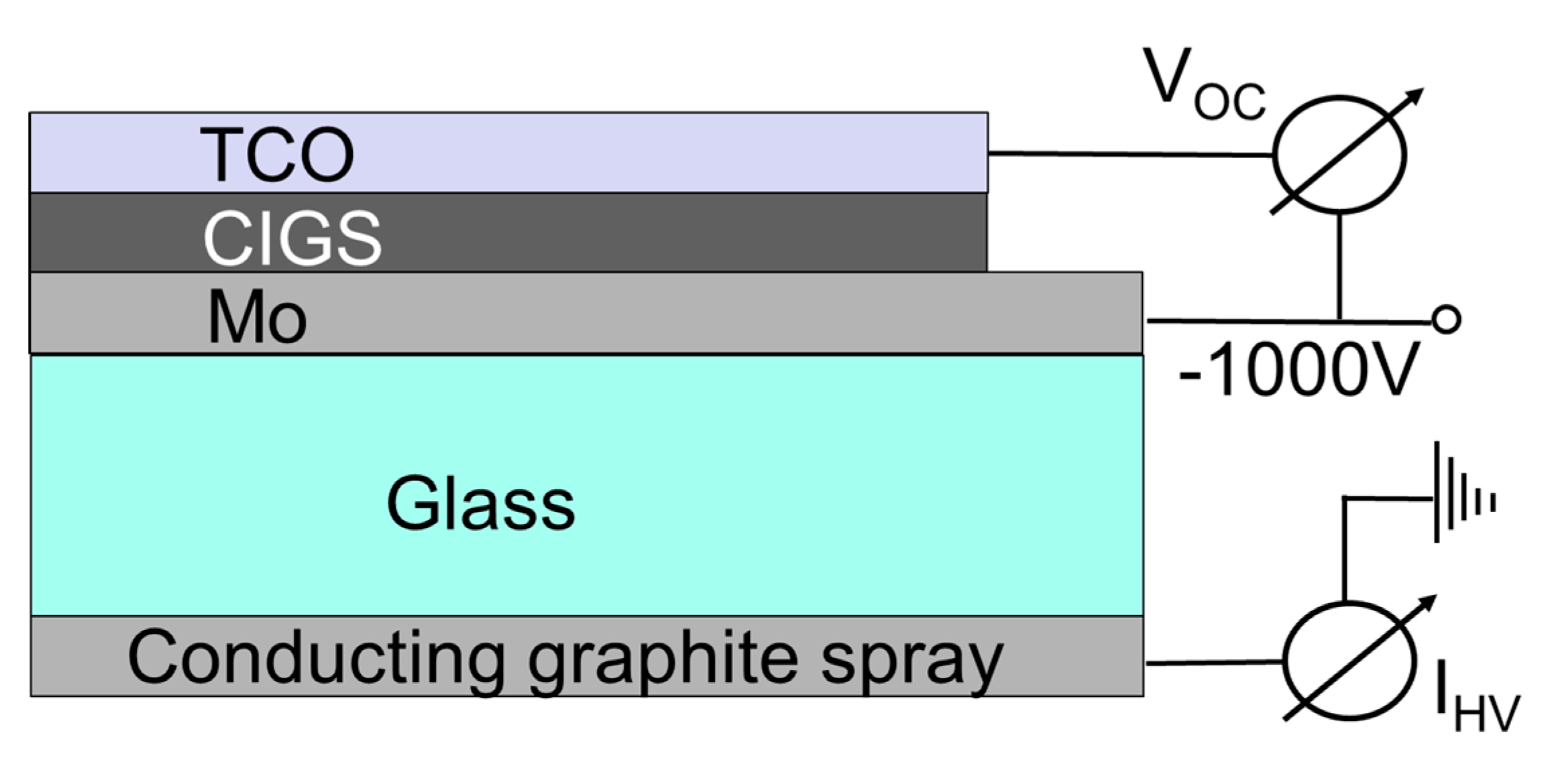
Figure 1 shows a schematic diagram of the layer structure and measurement setup for a CIGS solar cell. The cells were processed on soda-lime glass (SLG). The cell structure consists of sputtered Mo, co-evaporated Cu(In,Ga)Se
2, a wet chemical-processed CdS buffer layer, an i-ZnO layer, and a transparent conducting oxide (TCO) consisting of aluminum-doped ZnO (ZnO:Al). No further doping of the CIGS absorber prior to buffer deposition was performed, such as post deposition treatment with alkali metals [
5,
6]. Inline processes were used for the deposition of Mo, CIGS, i-ZnO, and ZnO:Al layers.
Two cell types were investigated here. The differences of both cell types are only based on changes in the Mo sputter process, whereas the Mo thickness was kept constant. All subsequent processes were conducted with equal process parameters. After initial findings that the Mo back contact plays a crucial role for the behavior under PID stress, cross-validation experiments were carried out with different suppliers of the Mo sputter target, with various sputtering plants and with different sputtering process parameters. There were two major findings: The correlation between PID immunity and Mo back contact could be confirmed and there is neither a unique sputtering recipe nor a key parameter in the sputtering process leading to PID-stable or -susceptible solar cells. Therefore, we investigated the differences in the resulting Mo back contact for PID-stable and -susceptible cells, in an attempt to identify the key parameter of the Mo back contact, which can be achieved by several different process parameters.
The substrate size was 10 cm × 10 cm. A Ni/Al/Ni grid was sputtered after TCO deposition and cells were patterned by mechanical scribing. Here, 1 cm laser edge deletion was applied on the substrates to avoid charge flow over the edges. A small part of the CIGS absorber was removed by mechanical scratching to obtain a Mo contact for applying a tinned copper ribbon with a silver conducting glue. Samples were prepared for the PID test by etching the backside up to the edges of the samples in 5% HCl to remove any conductive paths created by ZnO or CdS, and thoroughly rinsed with water afterwards. The backside of the substrate glass was then spray-covered by a conducting graphite paint (Cramolin GRAPHIT 1281411, ITW Chemische Produkte GmbH & Co. KG, Mühlacker, germany), only on the area that still contained Mo/CIGS/TCO after edge deletion. This procedure should have ensured a uniform voltage distribution.
The power supply unit for applying the 1000 V positive or negative bias was a FUG-type HCP 350-12500MOD. Measuring devices from IPC2U GmbH (Langenhagen, Germany) were used (I-7017) to measure the high voltage current. Humidity plays a major role for PID, as a moisture film on top of the glass surface acts as an equipotential surface, and thus facilitates current flow through the glass. The leakage current through the glass is a function of the relative humidity, the applied voltage, and the module’s absolute temperature [
7]. To exclude environmental influences, such as temperature, humidity, and the varying bias of a string due to the incoming light, tests were conducted in a Feutron-type 3436/15 climate chamber at low humidity (10%). The temperature was set to 70 °C and a defined high voltage was applied between the Mo back contact and the equipotential graphite layer on the back side of the substrate glass to test the cell stability against PID. The current–voltage (I–V) characteristics of CIGS solar cells were measured at 25 °C under 1000 W/m² simulated AM1.5G illumination (WACOM WXS-90S-5, Voss Electronic GmbH, Kirchheim-Heimstetten, Germany). Microscopic film morphology was characterized by high-resolution scanning electron microscopy (HR-SEM, XL30 SFEG system from FEI Deutschland GmbH, Dreieich, Germany). Surface film composition was analyzed with energy-dispersive X-ray spectroscopy (EDS, EDAX Team Apollo X in HR-SEM, Weiterstadt, Germany). For the Mo characterization, FIB lamellae were prepared in a Zeiss Crossbeam 1540 with Cryo-Stage. STEM images and EDX were performed with a Jeol ARM 200F high-resolution transmission electron microscope (TEM/STEM, Akishima, Japan) with a CEOS Cs corrector. EBIC measurements were carried out on freshly cleaved cross-sections of CIGS solar cells with a transimpedance amplifier. No further treatment, mechanical polishing or chemical etching, was applied to the samples prior to the EBIC measurements in junction configuration.
GDOES measurements were done with a GDOES Profiler 2 from Horiba Jobin Yvon (Bensheim, Germany). An RF source enables the measurement of insulating samples. However, the graphite varnish on the back of the sample strongly influences RF coupling. Therefore, the sputter power must be increased for all measurements to obtain adequate sputter rates. A cooling system maintains a low temperature to prevent a temperature induced diffusion of alkali ions during measurement. Because GDOES is a destructive analysis technique, the depth profile was recorded outside of the cell region.
CV profiling was performed at room temperature and in the dark on 0.5 cm2 cells with a grid on top by an impedance analyzer (Keithley 4200-SCS with a 4210-CVU card for AC measurements, Keithley, Cleveland, Ohio, U.S.A.), applying an AC voltage of 50 mVrms at 100 kHz and a varying DC bias. An equivalent circuit model employing a capacitance and a parallel resistance was applied to yield the capacitance and the conductance of the cell.
3. Results
The two different cell types, consisting only of different Mo back contacts, were exposed to a defined high voltage, which was applied between the spray-coated conductive graphite substrate backside and the Mo back contact of the cell. If the Mo back contact was operated as an anode (+1000 V), no damage of our cells was observed (not shown). Furthermore, a charge displacement by an AC voltage (250 V) causes no observable harm to the cells.
However, for a high negative external potential (e.g., −1000 V, with Mo back contact as the cathode) applied between Mo and the backside of the substrate, the photovoltaic performance decreases severely after a certain amount of electrical charge is driven through the substrate for one cell type, whilst the other cell type shows only minor parameter drifts. In our setup, as described above, within the climate chamber (70 °C and 10% relative humidity (R.H.)), the current due to the high voltage (HV) (−1000 V) remained constant for the cells on 3 mm soda-lime glass over several hours (the current was around 35 nA/cm²).
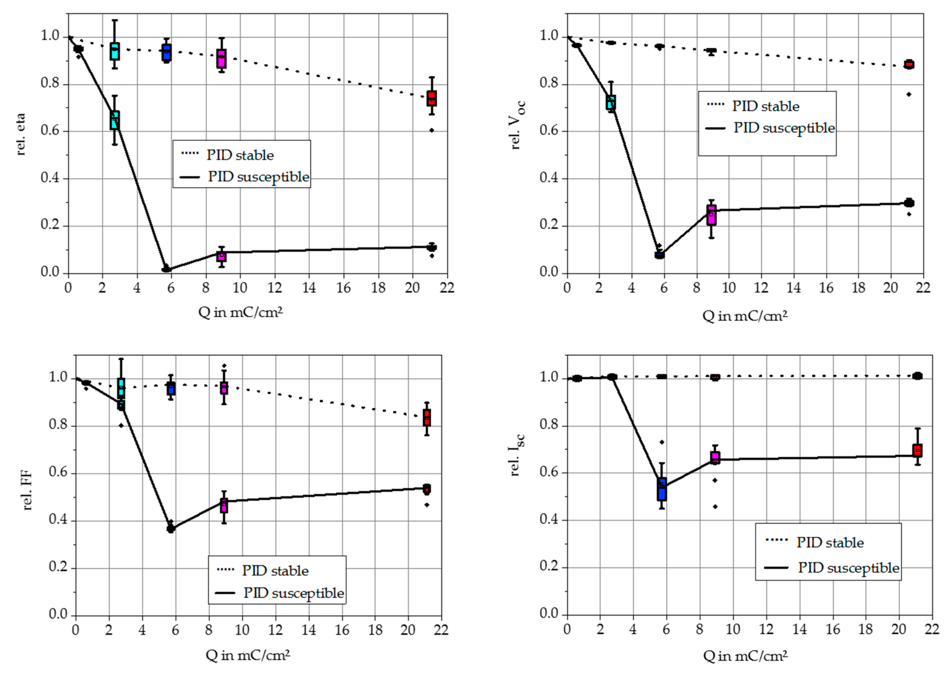
Figure 2 shows the I–V characteristics of the two different cell types during progressive charge transfer due to a negative high voltage exposure. The first measurements were very similar to the as-grown value. For PID-susceptible cells, longer stressing times decreased the open circuit voltage (
Voc), and as a consequence also the fill factor (FF).
At higher charge transfers, the short-circuit current (
Isc) also decreased dramatically. For the cells with increased PID stability, denoted as PID-stable, there is only a very slight shift in
Voc and
FF. However, after a large amount of charge (21.1 mC/cm²) has been transferred through the substrate, there is also an efficiency drop down to 74% of the initial value. This effect can also be seen in the diagrams of
Figure 3. Here, the boxplot for 10 cells and their evolution over the transferred charge (which is equivalent to the time due to the constant current through the glass) is shown. The efficiencies (eta) for the cells before HV exposure were in the range of 16% (median of the ten cells was 15.8% for PID-stable cells and 16.5% for PID-susceptible cells;
Voc: 695 mV and 705 mV;
Isc: 14.8 mA and 14.5 mA;
FF 72% and 75% for the stable and susceptible cells, respectively).
The two different types of Mo were examined by preparing FIB lamellae from the finished cell stacks before HV exposure in the FIB-SEM. The final thinning was performed under cryogenic conditions.
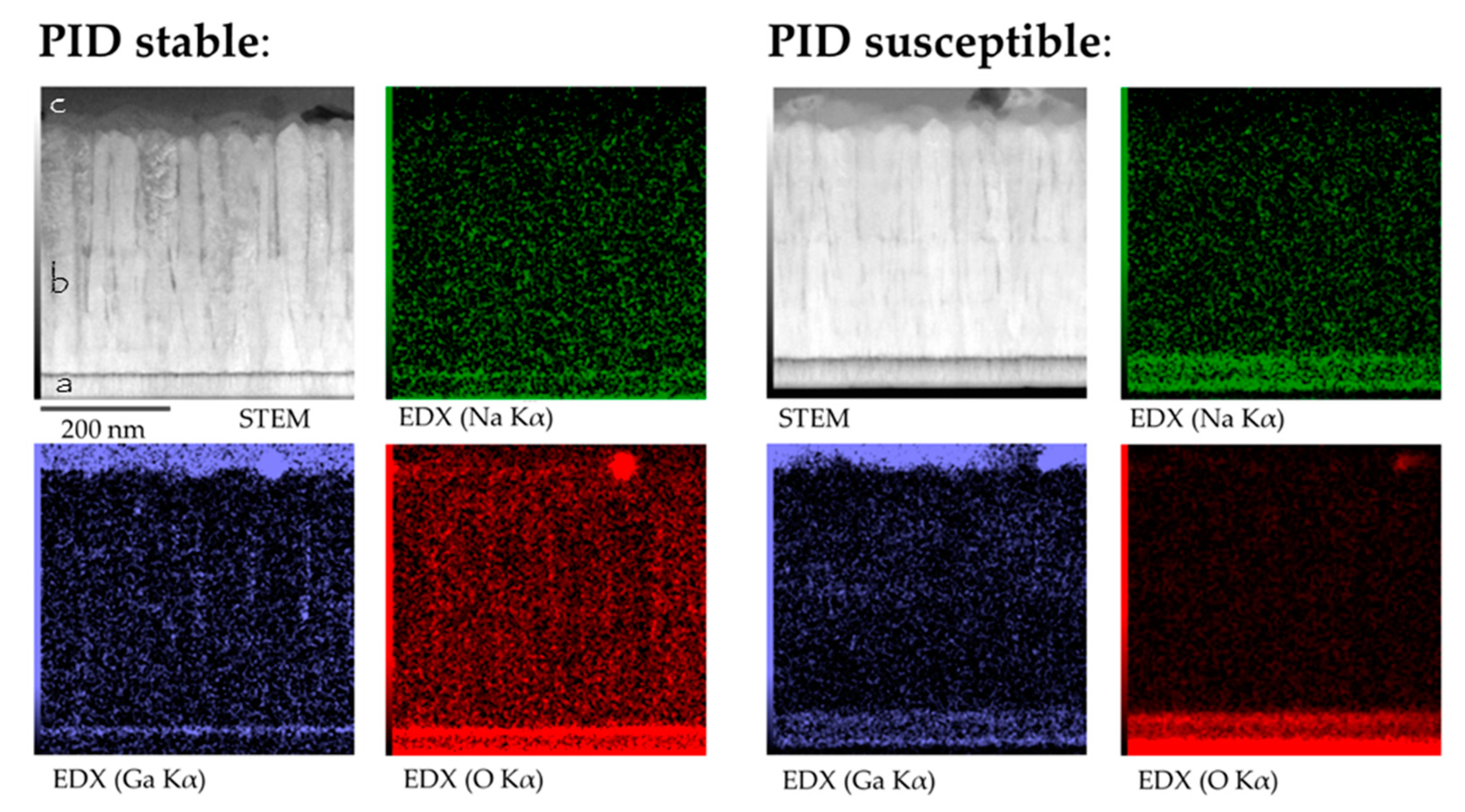
Figure 4 shows the STEM and EDX images taken of the lamellae from both Mo types in the high-resolution analytic TEM. The grain size and thickness of both Mo types are similar, as can be seen in the STEM images. The Mo for both variations was sputtered in two layers consisting of a thin seed layer followed by a thicker main layer (
Figure 4). As the Mo back contact is grown in an inline process passing through multiple Mo targets, growth disturbances are visible to some extent. As a general rule, the crystallites are continuous and columnar and the morphology of both samples is not conspicuously different. However, the Mo crystallites of the PID-stable cell seem to be slightly smaller and less dense, with a somewhat larger distance between the crystallites compared to the PID-susceptible Mo. Looking at the EDX results, the grain boundaries of the PID-stable Mo have a much higher oxygen content in comparison to the PID-susceptible cell. Furthermore, the sodium and gallium content seems to be increased in the Mo seed layer of the susceptible cell.
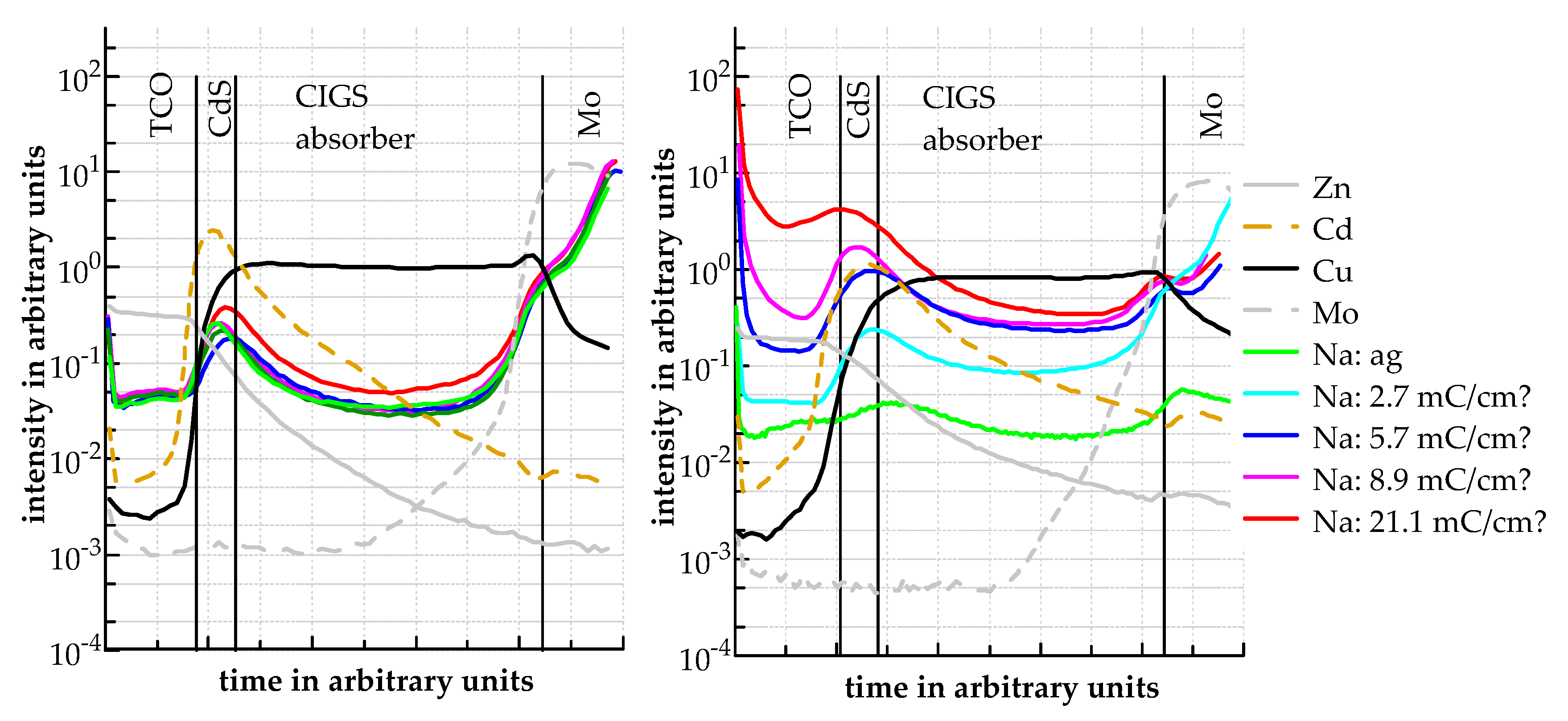
GDOES depth profiles at different times of HV exposure on the two cell types are shown in
Figure 5. For the PID-stable cells, almost no changes in composition were found. Only after a very high charge flow through the substrate (21.1 mC/cm
2 after 168 h of HV exposure) was sodium (Na) slightly increased in the CdS and absorber. No other elemental changes were observed. For PID-susceptible cells, an increase of Na at the back contact is observed after 5 h HV exposure (0.6 mC/cm²), while all other CIGS elements remained constant.
As the glass also contains other alkali elements in particular potassium, this element was also observed with GDOES. The potassium depth profile did not change during the whole experiment (not plotted in the graphs). After 21 h (2.7 mC/cm²), the Na signal is increased in the CIGS absorber and starts to accumulate in the CdS with increased HV exposure. After 45 h (5.7 mC/cm²) and higher exposure time of 71 h (8.9 mC/cm²), Na also segregates at the ZnO:Al surface. In addition, darker spots on the surface can be observed by visual inspection after a very high charge flow (21.1 mC/cm²). The samples were treated up to a charge of 42 mC/cm² and the spots were investigated with SEM and EDX.
Figure 6 shows a SEM image of such a spot and the EDX atomic ratios of selected areas. Na and carbon is enriched in the areas 2 and 3 within the spot. Probably, Na reacts with surface water and carbon dioxide from the air to form Na carbonate. Also in area 3, sulfur from the CdS buffer layer is detected on the surface, indicating that the ZnO:Al TCO layer was penetrated and demolished at this position.
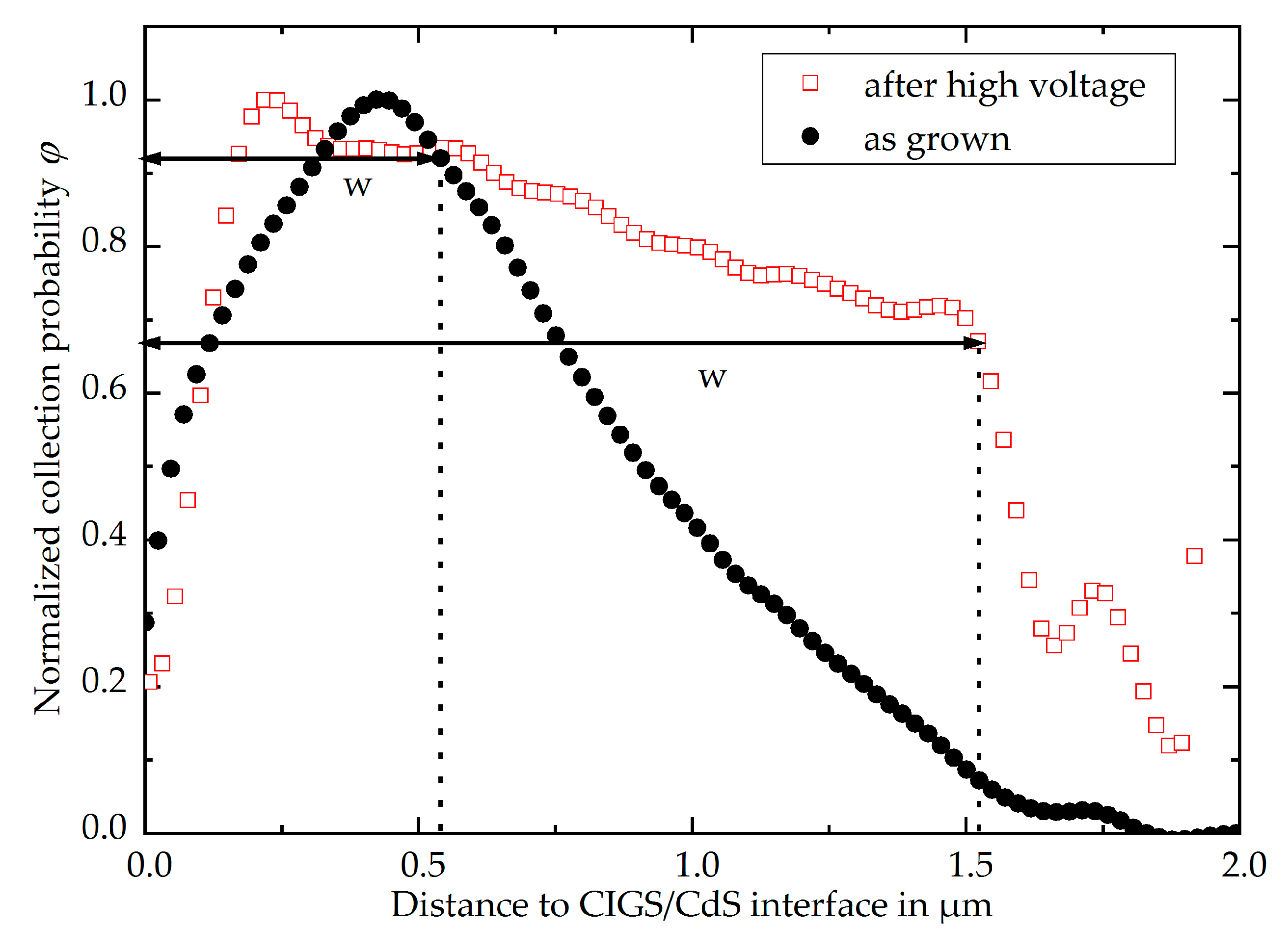
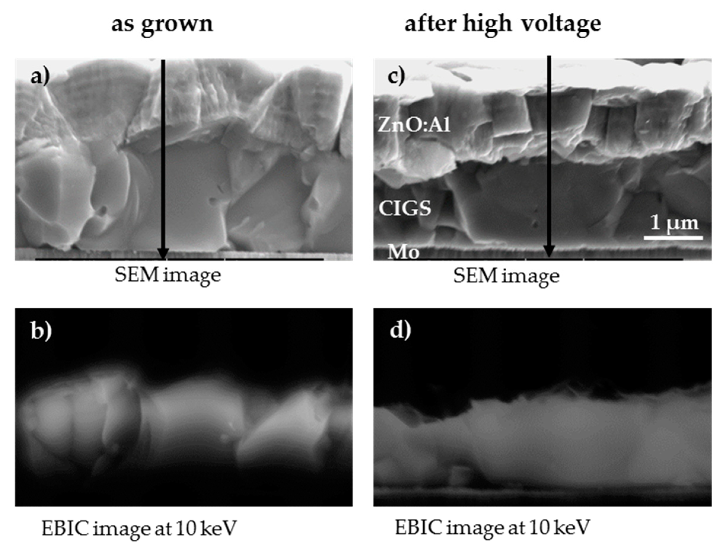
Figure 7 shows correlative SEM and EBIC images from a damaged CIGS grain of a PID-susceptible cell after application of HV compared to an undamaged one from the same sample in the as-grown state. The calculated collection probabilities at 10 keV electron energy shows a space charge region of 500 nm for the undamaged grain, whereas after HV exposure, the space charge region is enlarged up to 1.5 µm to the Mo back contact (
Figure 8).
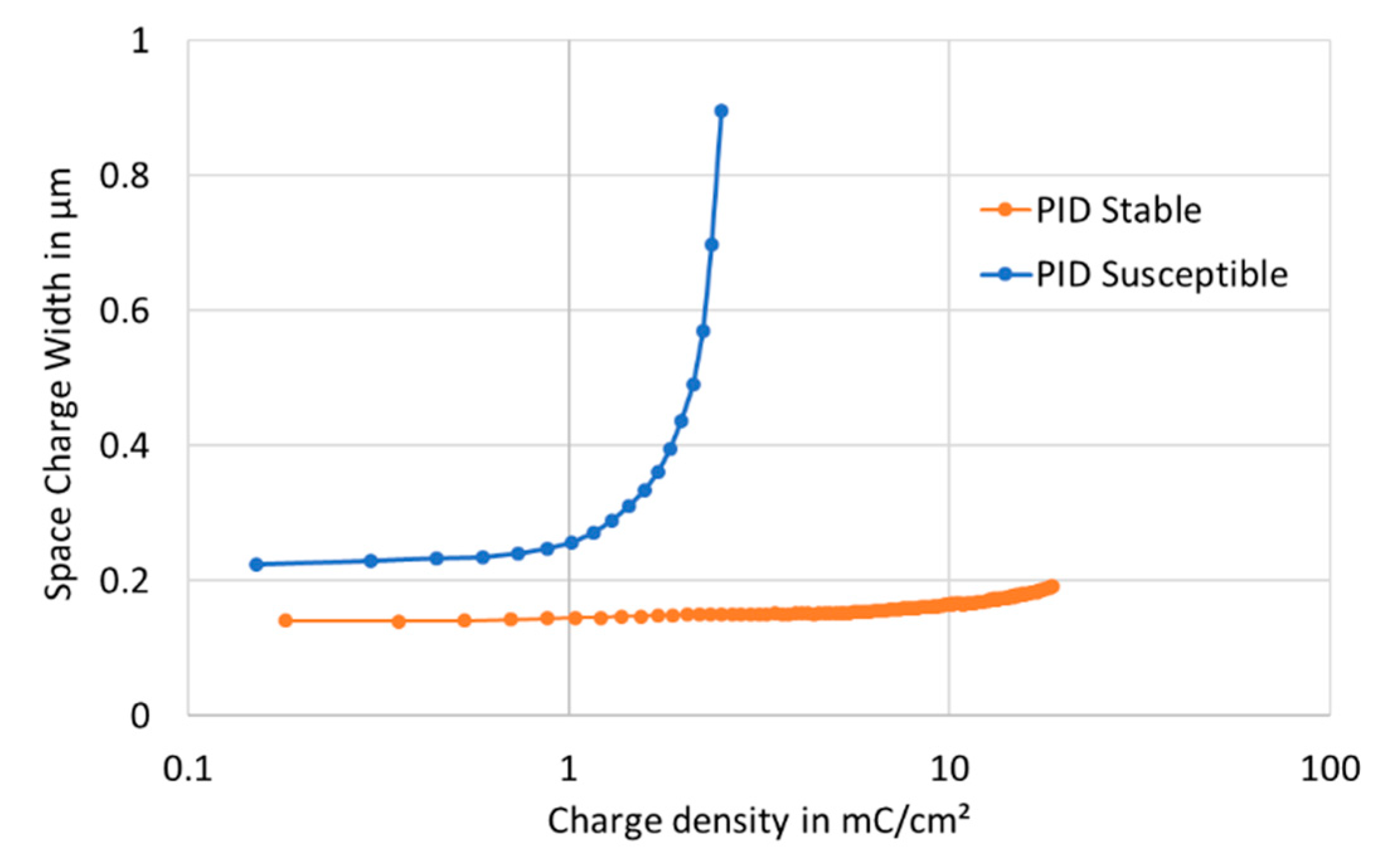
Figure 9 shows the evolution of the space charge width at 0 V measured by CV profiling against the charges due to HV exposure for a PID-susceptible solar cell and a PID-stable device. These results confirm that for PID-susceptible devices, the space charge width is enlarged as a consequence of a prolonged HV exposure. For the PID-stable device, only a minor increase in space charge width is observed, which is a well-known feature of the metastable behavior of CIGS-based solar cells.
It is interesting to note that in the initial state (prior to PID treatment), the PID-stable device apparently exhibits a smaller space charge width. However, it is not clear why the modification of the Mo leading to a PID-stable device also affects the doping level. The evolution of the space charge width is in agreement with the EBIC results presented in
Figure 7.
4. Discussion
We examined two different CIGS cell types. One was susceptible to PID if the Mo back contact was operated as a cathode, while the other showed significantly increased stability versus PID. After a certain amount of transferred charge, the PID-susceptible cell starts to degrade. Lechner et al. also reported a relationship between charge and degradation for a negative bias for full-size CIGS thin-film modules in the field [
8]. Performance changes of CIGS PV modules under high negative voltage are confirmed by Boulhidja [
9], Hacke [
10], and Liu et al. [
11]. Sakurai et al., however, reported no effect for negative bias in the field for their tested chalcopyrite-based Cu(In,Ga)(S,Se)
2 modules and used positive bias, which has been found to be easier to invoke changes in maximum power, if any (changes are in the range of ±2%) [
12]. They also mention that this polarity differs from other reports.
In our results, the PID-susceptible cells exhibit a strong degradation of
Voc, and as a consequence the
FF after exposure to high negative voltages.
Isc was also affected at the end of the degradation. A similar trend was shown by Fjällström et al. [
13] on float glass. They also showed that for cells on Na-free glass, no degradation was observed. We could confirm that finding on alkali-free glass, and can add that in our PID test setup, no current flow due to high voltage could be measured (not shown). The alkali-free glass was a good insulator, and therefore no charge was transferred through these substrates. A similar finding was reported by Muzzillo et al. [
14]. They used less conductive potassium-rich borosilicate glass (BSG) substrates, which led to 35× lower leakage current due to high voltage. However, after physically driving equal amounts of cations into the devices, the SLG and BSG substrates in their study had similar degradation in performance. The PID-stable cells in our experiment, however, were stable despite a high amount of charge being transferred through the glass substrate. Muzillo also shows CIGS devices that took much longer to fail (5× compared to their standard devices). Their improved devices employed an additional Al
2O
3 barrier layer between SLG and the Mo back contact. Their standard and Al
2O
3 samples both exhibited similar leakage currents [
15]. It is remarkable that in our findings, the transferred charge, and therefore the stability against, PID could be extended to more than 10× without a barrier layer just by changing the Mo back contact (this paper).
The sodium distribution differed after high negative voltage exposure for PID-susceptible cells and PID-stable cells. For PID-stable cells, almost no change in sodium distribution was found, whilst for PID-susceptible cells, significant changes in sodium distribution appear. Here, sodium starts to accumulate at the back contact (and to some extent the sodium concentration increases within the whole CIGS absorber), then increases in the CIGS absorber and starts to accumulate in the CdS, and with increased HV exposure finally segregates at the ZnO:Al surface to also form darker spots on the surface. Spot formation was also observed for CIGS absorbers exposed to a few hours of damp heat or for several months in ambient atmosphere, and significant amount of Na was found at the spot formations [
16,
17]. Sodium accumulation in the CdS was also observed by Fjällström after high voltage exposure, but only in the upper region of the CIGS absorber, not in the whole stack [
13]. Muzzillo also states that PID is due to physical accumulation of ions in the junction and verified this with secondary ion mass spectroscopy (SIMS) measurements [
14]. Harvey et al. confirm that sodium migrates through the absorber and accumulates at the CIGS–buffer interface upon PID stressing, while only a small change in potassium in the CIGS distribution was found with time of flight secondary ion mass spectroscopy (TOF-SIMS) on CIGS modules [
18].
In our experiments, we could clearly correlate the stability against PID with the Mo back contact. However, we could not identify a key parameter of the sputtering recipe leading to stable devices. This is quite obvious, as we found that this stability correlates among others with the sputter target and with the sputtering plant in combination with adapted process parameters. Therefore, in our approach we investigated key characteristics of the Mo back contact, which should be targeted by an appropriate and adapted deposition optimization. Our analysis of the Mo back contact revealed several differences, which might lead to the observed immunity against PID.
This analysis shows higher oxygen and gallium contents within the Mo for the PID-stable cell (as shown in
Figure 4 above) in combination with a less dense and more open granular structure, which might lead to a higher diffusion of gallium and oxygen, most probably along the grain boundaries of the Mo. The impact of these characteristics on the diffusion of Na during the PID stress into the CIGS (and the CdS buffer layer) is subject to future investigation. The oxygen might trap Na, and thus hinder Na migration.
The EBIC and CV measurements on PID-affected cells both show that the space charge region is enlarged up to the Mo back contact and that the doping density is lowered by a negative potential. Acceptor concentration decreases, which qualitatively explains the
Voc drop in the I–V characteristics. Looking at
Figure 2, it is quite obvious that the initial degradation mainly affects
Voc as a result of a lower doping density or as a consequence of a lower minority carrier lifetime. However, considering the fact that in this initial state,
Isc (and also external quantum efficiency (EQE) (not shown)) remains constant (or increases slightly), a decreased minority carrier lifetime (with a smaller diffusion length consequently) can be excluded, leaving a decreased acceptor density as the most probable origin for the observed
Voc drop. This is also confirmed by the findings from Alonso-Garcia, who showed an increase of diode saturation current density and series resistance followed by a decrease in shunt resistance [
19]. The EBIC measurement (
Figure 7) shows a damaged CIGS grain compared to an undamaged one from the same sample. The calculated collection probabilities at 10 keV electron energy show a space charge region of 500 nm for the undamaged grain. This is in good agreement with prior measurements by Kniese and Witte on co-evaporated CIGS with a Ga/(Ga+In) ratio of 0.3 and a CdS/i-ZnO buffer system [
20,
21]. After exposure to HV, however, the space charge region is enlarged up to 1.5 µm (
Figure 8). CV profiling qualitatively confirms this picture (
Figure 9). The acceptor density is lowered for the HV-damaged sample, while the space charge region increases. According to these results, PID compensates acceptor states in the CIGS. Fjällström [
13] also performed CV investigations and found an increased space charge width after PID, which was reduced upon recovery [
22] for CIGS cells with a CdS buffer. They did not see any recovery, and therefore no reduction of the space charge width by recovery for CIGS cells with Zn(O,S) buffer layers.
An increase of Na with an associated decrease of the doping density seems to be in contrast with early findings, in which high efficiencies can be achieved due to Na diffusion into the CIGS absorber during the deposition process. The effect of Na here includes an improvement in p-type conductivity, and therefore improved V
oc and
FF [
23,
24]. However, Champness showed that a type inversion can occur for stoichiometric CuInSe
2 Bridgman crystals with a larger amount of Na [
25]. Thus, an excessive supply of Na can lead to an inferior cell performance. The Na depth profile and its concentration at the CIGS surface are very important in determining the properties of CIGS solar cells [
26].
Other authors examined the influence of a voltage between the front glass of the CIGS modules and the cells. Yamaguchi et al. show a degradation for an applied voltage between the front glass and cells for modules at negative voltage [
27]. Voswinckel also shows different behavior between the front and back glass [
28]. Alonso-Garcia states that PID through the front glass may be much less relevant than through the rear [
19]. Springer shows a strong influence of the encapsulant on the leakage current [
29]. Therefore, due to the much lower leakage current through the front glass, a much longer time to reach the accumulated charge threshold for degradation by applying a voltage across the front glass is observed. This finding fits well in the picture of Na-induced degradation.

