3.1. APS Coatings on Ox/Ox CMCs
Coatings of Y
2O
3, Gd
2Zr
2O
7, Y
3Al
5O
12 and Yb
2Si
2O
7 were applied on the untreated and cleaned substrates. XRD measurements of as-sprayed samples were carried out. The measurements are plotted in
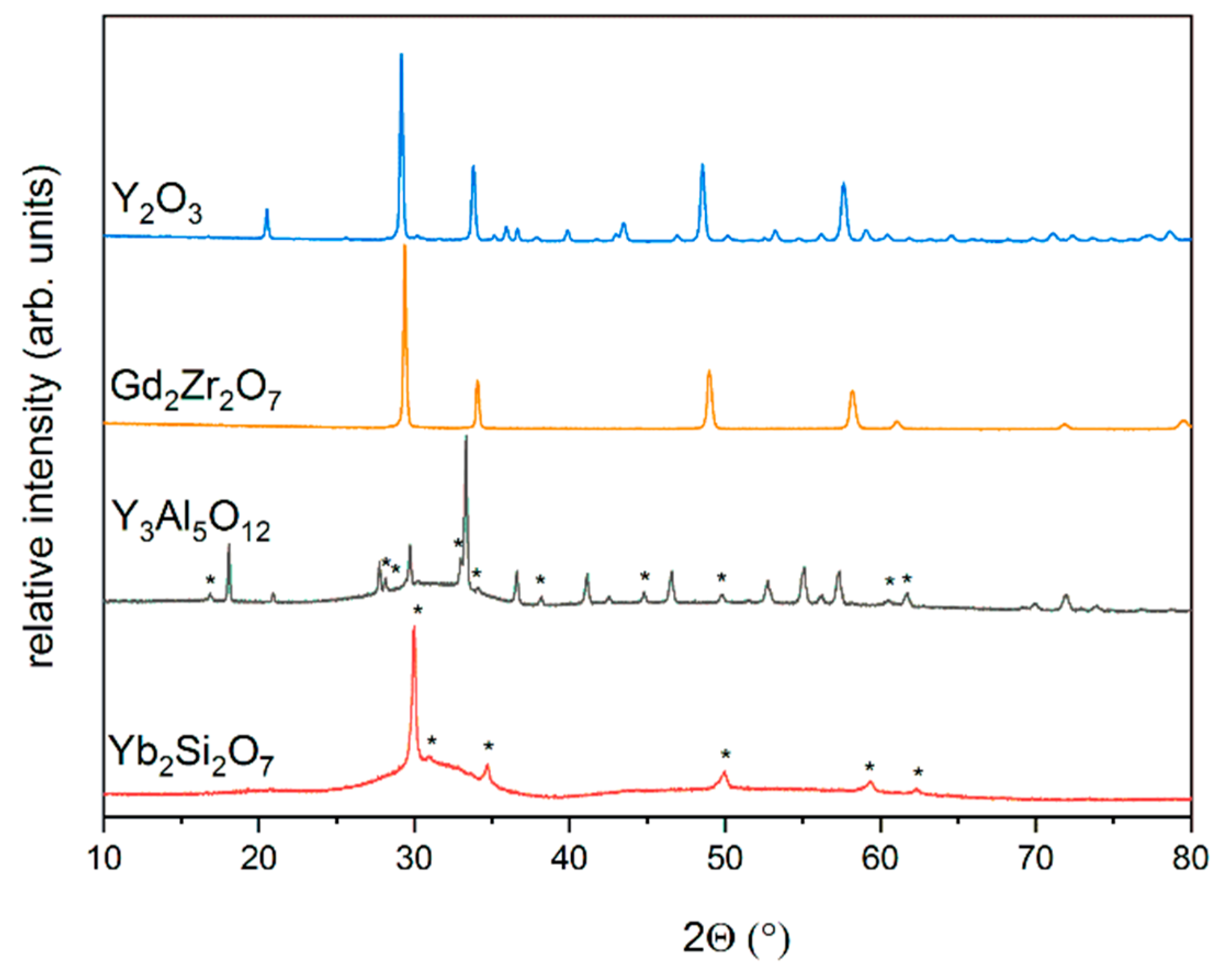
Figure 3, signals that cannot be attributed to the desired phase were marked with an asterisk (*). The XRD measurements of Y
2O
3 and Gd
2Zr
2O
7 show the diffraction patterns of the corresponding phases, no signals from secondary phases were observed. The coatings appear to have a high crystallinity. In contrast to this, the XRD measurements of Y
3Al
5O
12 and Yb
2Si
2O
7 coatings show humps, which indicate the presence of large amounts of amorphous phases. Due to the low crystallinity not all phases could be identified. The XRD measurements of the Y
3Al
5O
12 coating shows the diffraction pattern of Y
3Al
5O
12 and YAlO
3. The formation of the alumina depleted phase YAlO
3 is attributed to evaporation of alumina during the spraying process, since the vapor pressure of Al
2O
3 is higher than that of Y
2O
3 [
24]. The XRD measurement of the Yb
2Si
2O
7 coating shows no reflections of the desired phase. Besides the large amorphous hump, the diffraction pattern of Yb
2O
3 was observed. The high amorphous content of the Y
3Al
5O
12 and Yb
2Si
2O
7 coatings might cause crystallization stress in the coating during thermal treatment.
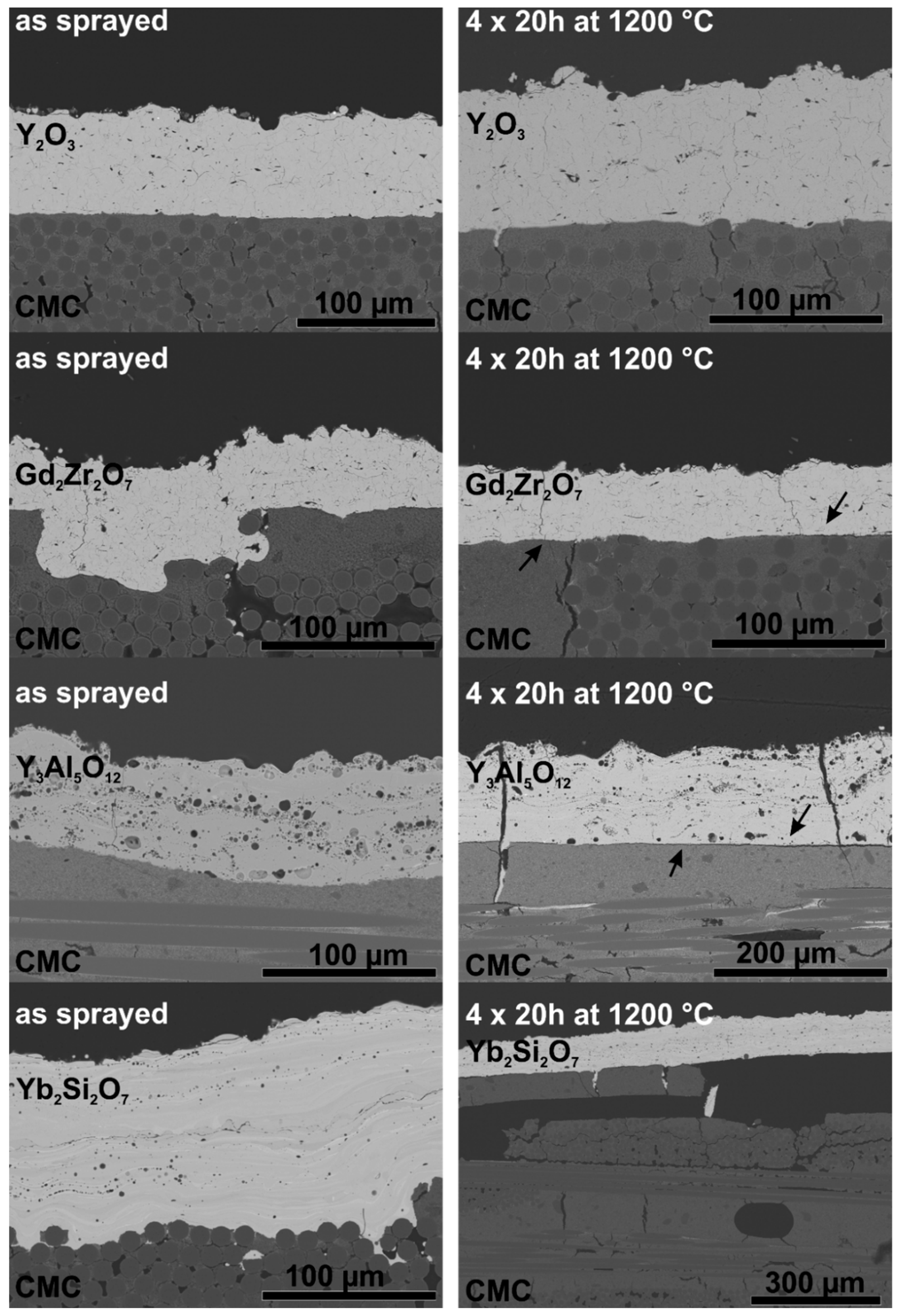
The as-sprayed samples were subjected to furnace thermal cycling, the used temperature program consists of four 20 h cycles at 1200 °C. SEM images of cross sections of samples in the as-sprayed state and after thermal cycling are presented in
Figure 4. Additionally, higher magnification images of the interface region of the coatings are presented in
Figure 5.
The obtained Y
2O
3 coatings were dense and fully crystalline. The adhesion of the Y
2O
3 samples seems to be quite good, after heat treatment no signs of cracks or delamination are observed. The good adhesion can be attributed small TEC mismatch and phase stability, resulting in low driving force for delamination. Another reason for the good adhesion is the formation of yttrium-aluminates at the coating substrate interface leading to chemical bonds between coating and substrate [
25]. In
Figure 5 the formation of several yttrium-aluminates known from the phase diagram [
26] can be observed.
The SEM images of the Gd
2Zr
2O
7 coatings show dense and homogenous coatings in the as-sprayed state.
Figure 5 shows the coating substrate interface in detail. After thermal cycling no sign of a reaction between Gd
2Zr
2O
7 and Al
2O
3 was observed. This is in contrast to Lakiza et al. [
27] and Leckie et al. [
28] The phase diagram of Gd
2Zr
2O
7, presented by Lakiza et al. [
27], suggests formation of gadolinium-aluminates such as GdAlO
3 and Gd
4Al
2O
9. The reaction between Gd
2Zr
2O
7 and Al
2O
3 to GdAlO
3 was observed in a study by Leckie et al. [
28]. The absence of this reaction in this study can be explained by bad wetting which causes only small contact areas to the substrate, as a consequence the reaction is inhibited. However, after heat treatment the coating was delaminated at the interface (marked by arrows in
Figure 4). This can be explained by the TEC mismatch (∆
CTE = 3 × 10
−6 K
−1, see Equations (2) and (3)) and bad wetting of the relative smooth substrate (
Ra = 2.6 µm).
The SEM images of the Y
3Al
5O
12 coating confirm the presence of secondary phases within the coating. Furthermore, large round pores can be observed in the Y
3Al
5O
12 coatings. The high porosity is not favourable for an EBC, as pores and cracks increase the permeability for water vapor. Despite the low TEC mismatch (∆
CTE = 3 × 10
−6 K
−1), the Y
3Al
5O
12 coatings tend to fail during thermal cycling. This can be explained by the high amorphous content of the APS-Y
3Al
5O
12 coatings. Thermal treatment leads to crystallization and phase transformation of the coating; this causes stress within the material leading to the formation of segmentation and delamination cracks. The formation of large pores in Y
3Al
5O
12 coatings was also reported by Weyant et al. [
29], a dependence between crystallization, substrate temperature and porosity was assumed. According to the phase diagram [
30] of Y
2O
3 and Al
2O
3, a reaction between coating and substrate is not expected. The SEM image of the Y
3Al
5O
12 - Al
2O
3 interface (
Figure 5) shows that unlike with Y
2O
3, no reaction occurs between substrate and coating.
The cross-sections show that the disilicate coatings have a lot of pores and consist of several phases, which is, again, not favourable for an EBC. Furthermore, crystallization problems occurred, as described for the Y
3Al
5O
12 coatings. Due to the high TEC mismatch (∆
CTE = 5.2 × 10
−6 K
−1, see Equations (2) and (3)) and the stresses that arise during crystallization, these coatings were delaminated during thermal treatment. According to the phase diagram of Yb
2O
3-SiO
2-Al
2O
3 [
31], the formation of mullite (Al
6Si
2O
13) and ytterbium-aluminates (Yb
4Al
2O
9, Yb
3Al
5O
12) during thermal cycling is possible. However, no reaction between coating and substrate was observed (see
Figure 5). The absence of a reaction layer may be attributed to the loose contact between coating and substrate as well as the high TEC mismatch and the resulting premature coating delamination.
Due to the high coating crystallinity, phase purity and coating density, Gd2Zr2O7 and Y2O3 were chosen for further experiments. Although Gd2Zr2O7 has a higher CTE mismatch, it is a desirable top coat due to its excellent CMAS stability. In order to increase the coating adhesion different methods of surface preparation were carried out before spraying.
First, samples of the Al
2O
3/Al
2O
3 CMC were mechanically treated to increase the surface roughness. Some samples of the Al
2O
3/Al
2O
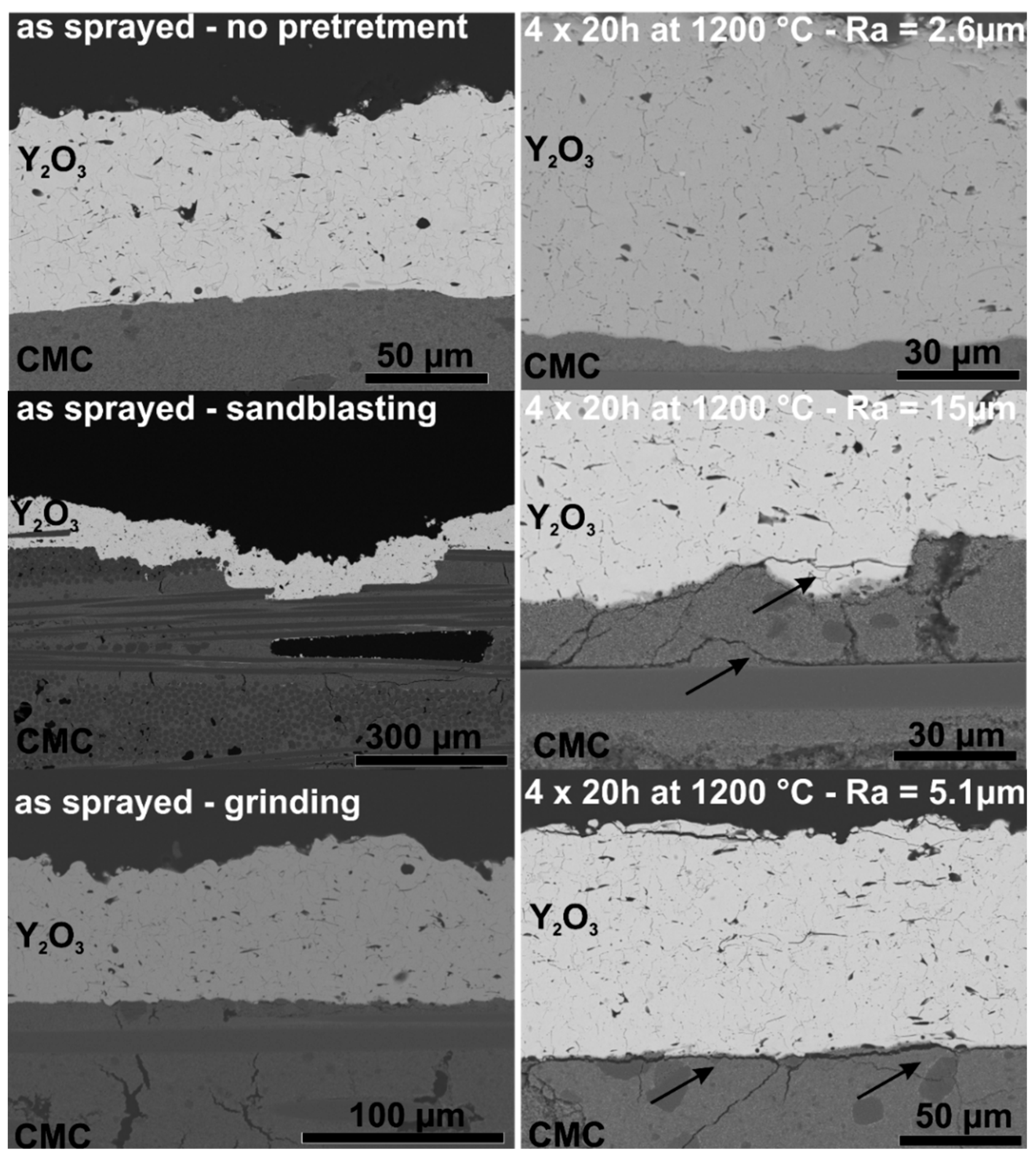
3 CMC were ground, others were grit-blasted. Both methods were able to increase the surface roughness from 2.6 µm to 5.1 µm and 15 µm, respectively. The samples were coated and subsequently furnace cycled for 4 × 20 h at 1200 °C. SEM images of cross-sections of the as-sprayed Y
2O
3-coatings as well as furnace cycled samples are shown in
Figure 6. The results show that the mechanical pre-treatment damaged the ceramic substrate to such an extent that even Y
2O
3 coatings failed. Unlike in the study of Gérendas et al. [
32], mechanical pre-treatment was not able to achieve sufficient coating adhesion on this CMC.
Laser ablation was used for surface structuring without damaging of the substrates. The positive effect of laser surface structuring of Al
2O
3/Al
2O
3 CMCs on coating adhesion was recently demonstrated by Gatzen et al. [
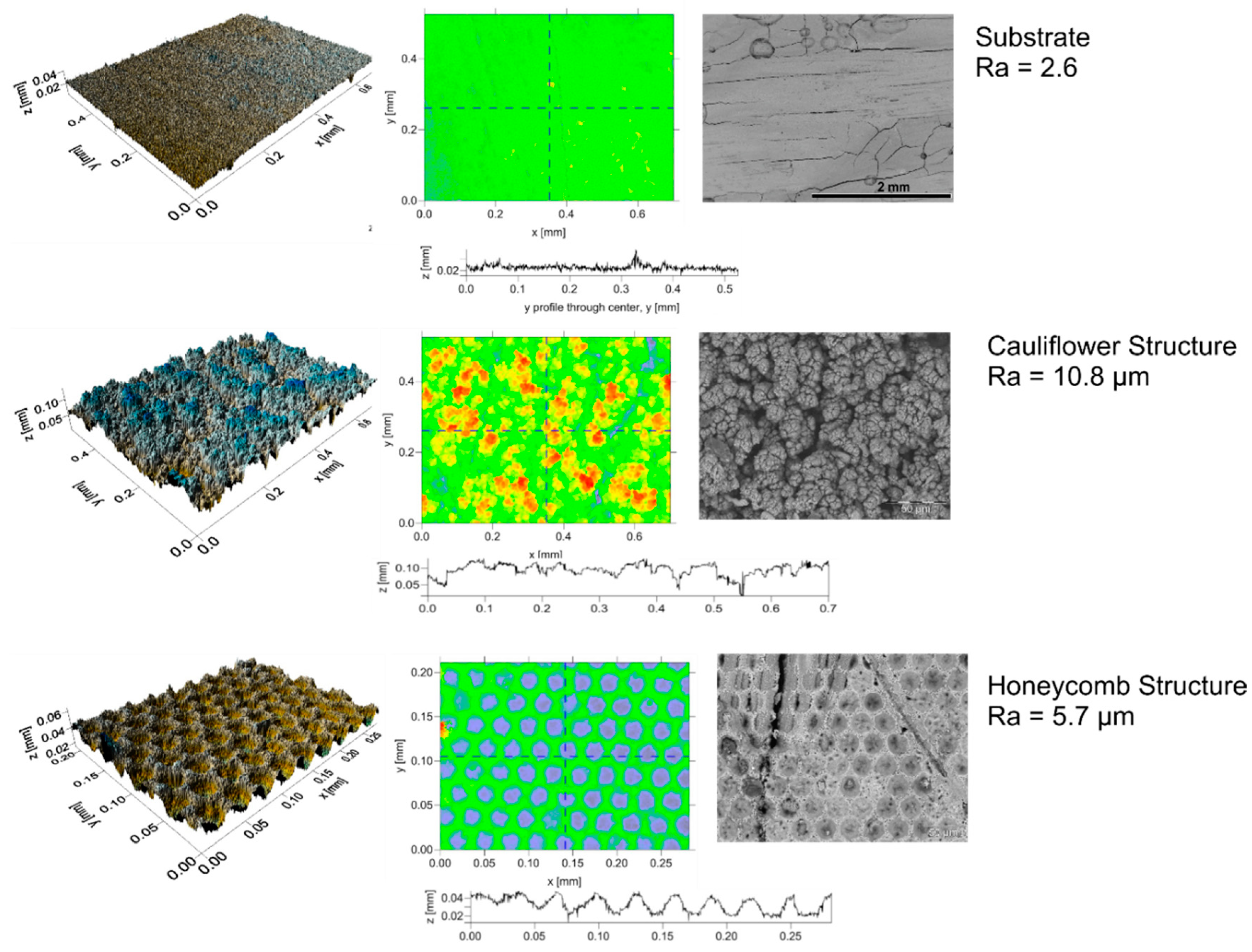
23]. Two different structures were chosen for this study: honeycomb and cauliflower structure. Both structures are illustrated in
Figure 7.
The untreated substrate has a roughness of about 2.6 µm and a homogenous smooth surface. Few cracks and pores at the surface offer possibilities for clamping. The cauliflower like surface structure comprises an irregular and inhomogeneous surface of re-solidified alumina. An average roughness of 10.8 µm was achieved with this pattern. The honeycomb structure shows well- defined holes close to each other. A roughness of about 5.7 µm was measured for this pattern. Both surface structures offer more possibilities for clamping, therefore, an increase in lifetime is expected especially for Gd2Zr2O7 coatings.
After structuring the samples were coated with Y
2O
3 and Gd
2Zr
2O
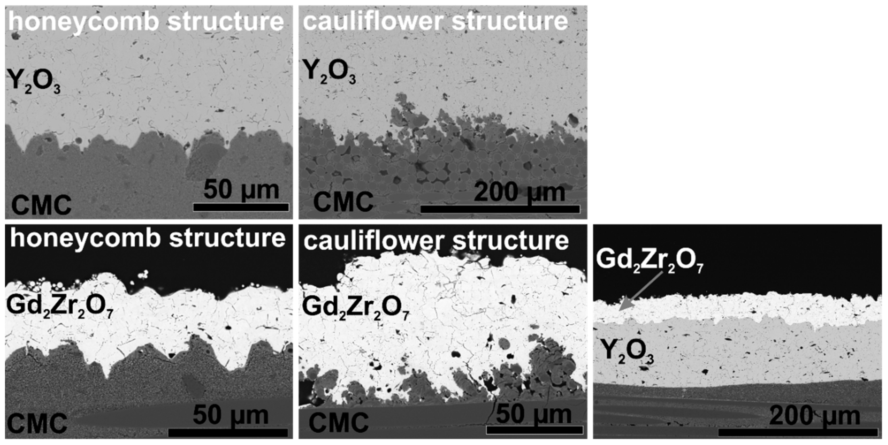
7. SEM images of the coated and thermally cycled samples are shown in
Figure 8. Both coatings could infiltrate the voids in between the substrate structure. The surface structures, especially the cauliflower structure, allow interlocking of the coating. After thermal cycling no cracks or delamination occurred in the Y
2O
3 coating-substrate-system. This shows that in contrast to grit-blasting and grinding, laser structuring of the CMC does not weaken the ceramic matrix. Furthermore, after thermal cycling of the laser-structured Gd
2Zr
2O
7 coated samples, the coating-substrate interface shows no delamination cracks. This is a significant improve, compared to the coating on untreated substrates. Although the energy release rate is high in these coatings with high mismatch (see Equations (2) and (3)), the laser structuring of the samples proofed to be beneficial for the coating adhesion (e.g., the critical energy release).
In addition, a third method of adhesion improvement was tested for Gd
2Zr
2O
7: the usage of an Y
2O
3-bondcoat. For this, the untreated substrate was first coated with Y
2O
3 and then coated with Gd
2Zr
2O
7. This double layer coating system is referring to the double layered TBCs as published by Vaßen et al. [
33]. The Y
2O
3-bondcoat helps to buffer to some extent especially at edges the CTE mismatch between the CMC and Gd
2Zr
2O
7. Furthermore, the Y
2O
3 coating is known to be good adherent on Alumina CMCs [
25] and offer a rough surface for the Gd
2Zr
2O
7 coating. Using Y
2O
3 as an interlayer between substrate and Gd
2Zr
2O
7 also proofed to increase the coating adhesion as well.
3.2. Development of APS Y2SiO5 coatings
According to
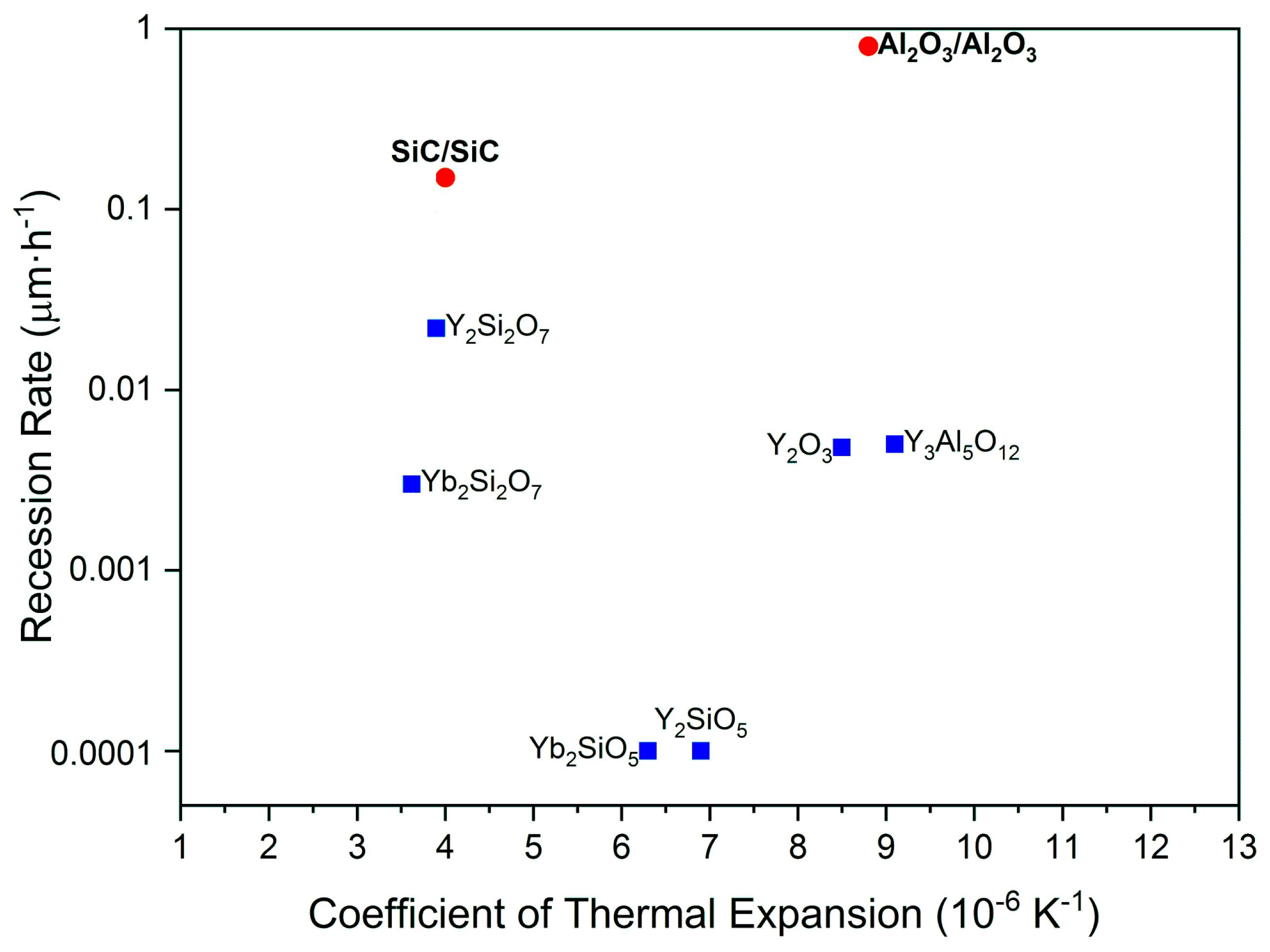
Figure 1 Y
2SiO
5 has an excellent water vapor resistance and is therefore considered as appropriate EBC material [
34,
35]. In this investigation only rather hot APS spraying conditions are investigated for this material. The density of all the coatings manufactured by the investigated conditions (see
Table 2) has been rather high, more interesting is the phase content which shows remarkable differences (see
Figure 9). Compared to the He as secondary gas, hydrogen increased the plasma enthalpy which leads to higher substrate temperatures (750°C) and increases the amount of crystallization. The comparable amount of SiO
2 in all coatings might indicate no significant differences in the silica loss during spraying (although the amorphous content is not considered).
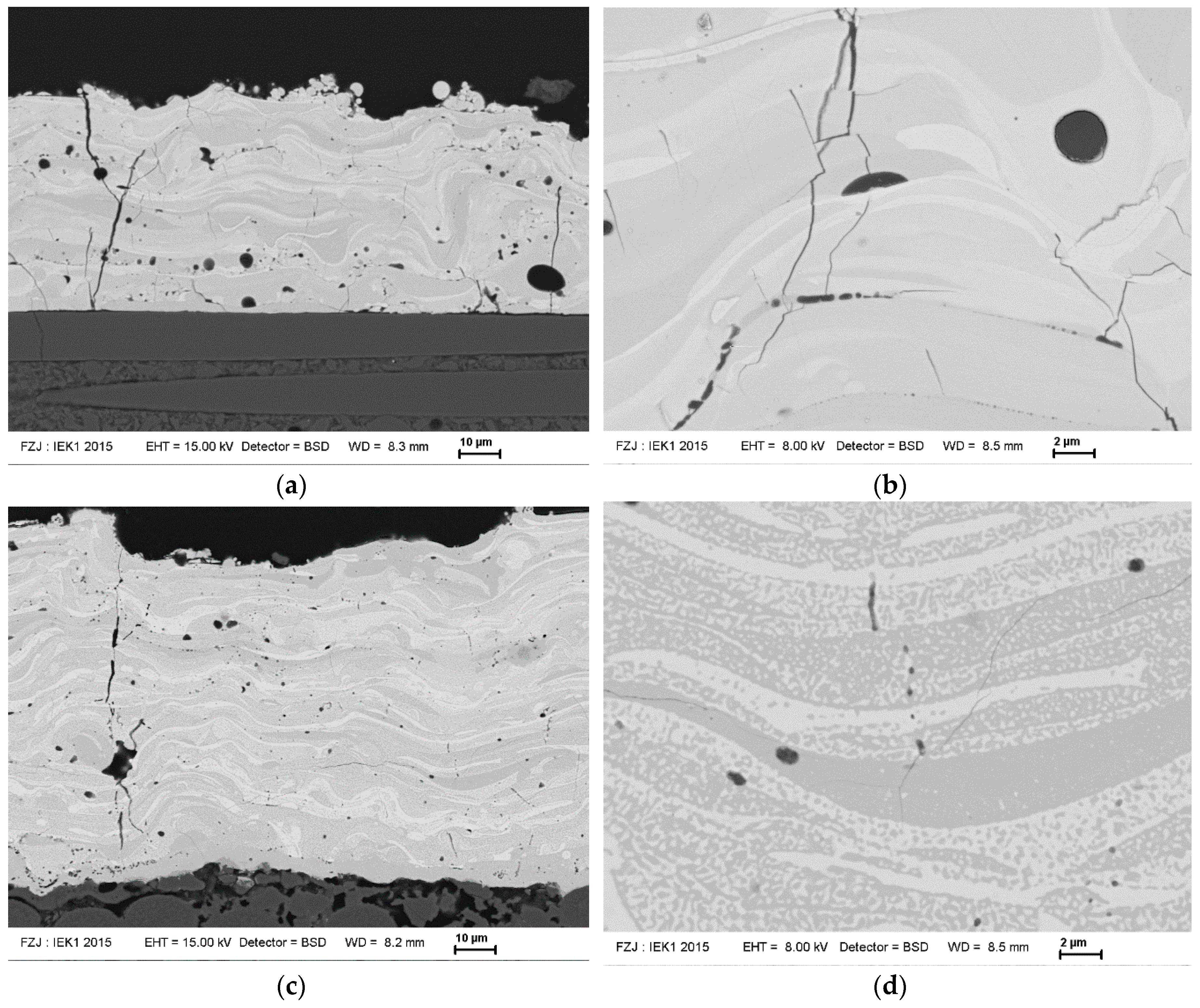
Due to the highest crystallinity, the condition D with hydrogen and long stand-off distance (condition D) was used for further studies and coatings on C/SiC substrates were prepared. In
Figure 10 SEM micrographs of the coatings in the as-sprayed condition and after annealing for 12 h at 1350 °C. First of all, the coating is also after the heat-treatment well-adherent. This indicates that the TEC mismatch (see Equations (2) and (3)) between coating and substrate seems to be not extremely detrimental (although the material would fit even better to Ox/Ox CMC substrates). In addition, also the phase transformation at 850 °C and the strongly anisotropic expansion of Y
2SiO
5 [
36] obviously does not significantly affect coating integrity.
In addition, the size of the segmentation and micro cracks is largely reduced due to sintering, some segmentation cracks are even no longer penetrating through the whole coating. Also the phase distribution changed significantly. While in the as-sprayed condition rather large regions with low and high silicon content appear (stemming from the impinging particles which have lost silicon during spraying mainly at their surface), the annealed coating shows much finer phases consisting of cubic Y
2O
3 (bright) and monoclinic Y
2SiO
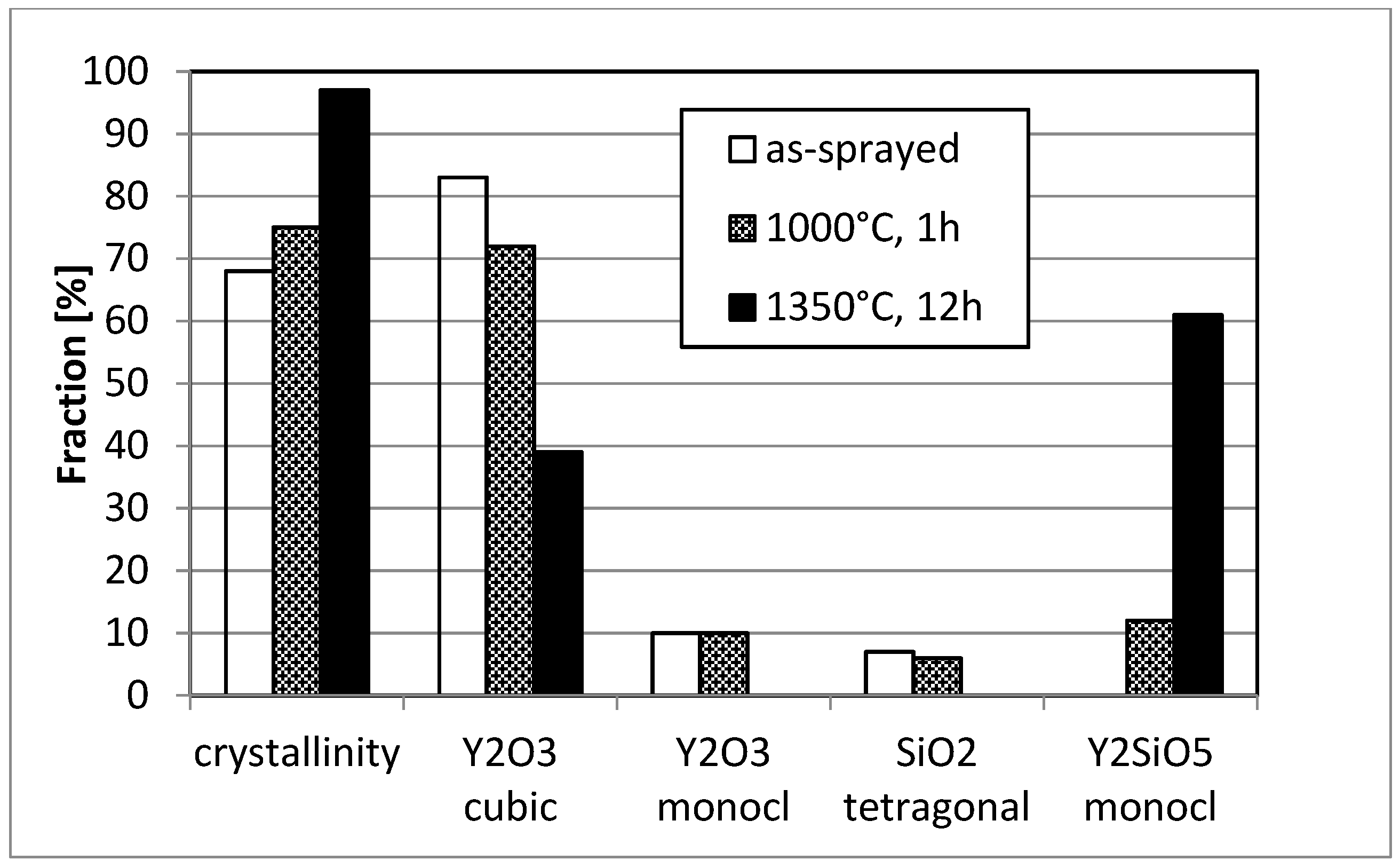
5 (darker). The evolution of phases is shown in
Figure 11 measured by XRD and using Rietveld refinement. Obviously, a short-term annealing at 1000 °C is not sufficient to form the equilibrium phases. As the coating is rather dense, the Y
2O
3 as a second phase has a reasonable corrosion resistance (
Figure 1) and the microstructure probably will show some particulate toughening effects, the found coating is expected to perform good as EBC.
3.3. Yb2Si2O7 Coatings Manufactured by Different Thermal Spray Techniques for SiC/SiC Substrates
Figure 12 shows the phase composition of APS, HVOF and VLPPS coatings deposited from different particle size fractions of the same Yb
2Si
2O
7 feedstock. The main differences between the different methods are melting degree of the sprayed particles and deposition temperatures which define the crystallinity of the coatings as well as the degree of Si evaporation during spraying.
In APS and VLPPS, as a result of the high heat transfer from plasma to the particles, particles melt, impact on the substrate in the molten state and rapidly solidify on the substrate. High plasma powers were selected in the deposition of EBCs with APS (57 kW) and VLPPS (90 kW) as a dense microstructure consists of well-flattened particles with good interfacial contact is aimed. While high plasma powers ensure melting of particles in the plume, it also leads to a significant amount of Si-evaporation from Yb
2Si
2O
7 during spraying. As a result of that, Si-depleted secondary phases such as Yb
2SiO
5 and Yb
2O
3 are found in the as-sprayed coatings as shown in the
Figure 12a. Furthermore, due to quenching of the molten particles on the substrate, that is at nearly room temperature if not pre-heated by plasma plume, crystallization of the glass forming silicates is suppressed and the amorphous phase is formed. The APS experiments carried out in order to increase the SiC substrate temperature by heating with plasma prior to deposition revealed that for a substrate size of 50 × 50mm
2, it is possible to increase the substrate temperatures up to about 800–900 °C however the temperature rapidly goes down to 500–550 °C till the deposition starts. As shown in
Figure 12a, this deposition temperature range was found to be not sufficient to activate and complete the crystallization of the coating. According to HT-XRD analysis of amorphous plasma-sprayed Yb
2Si
2O
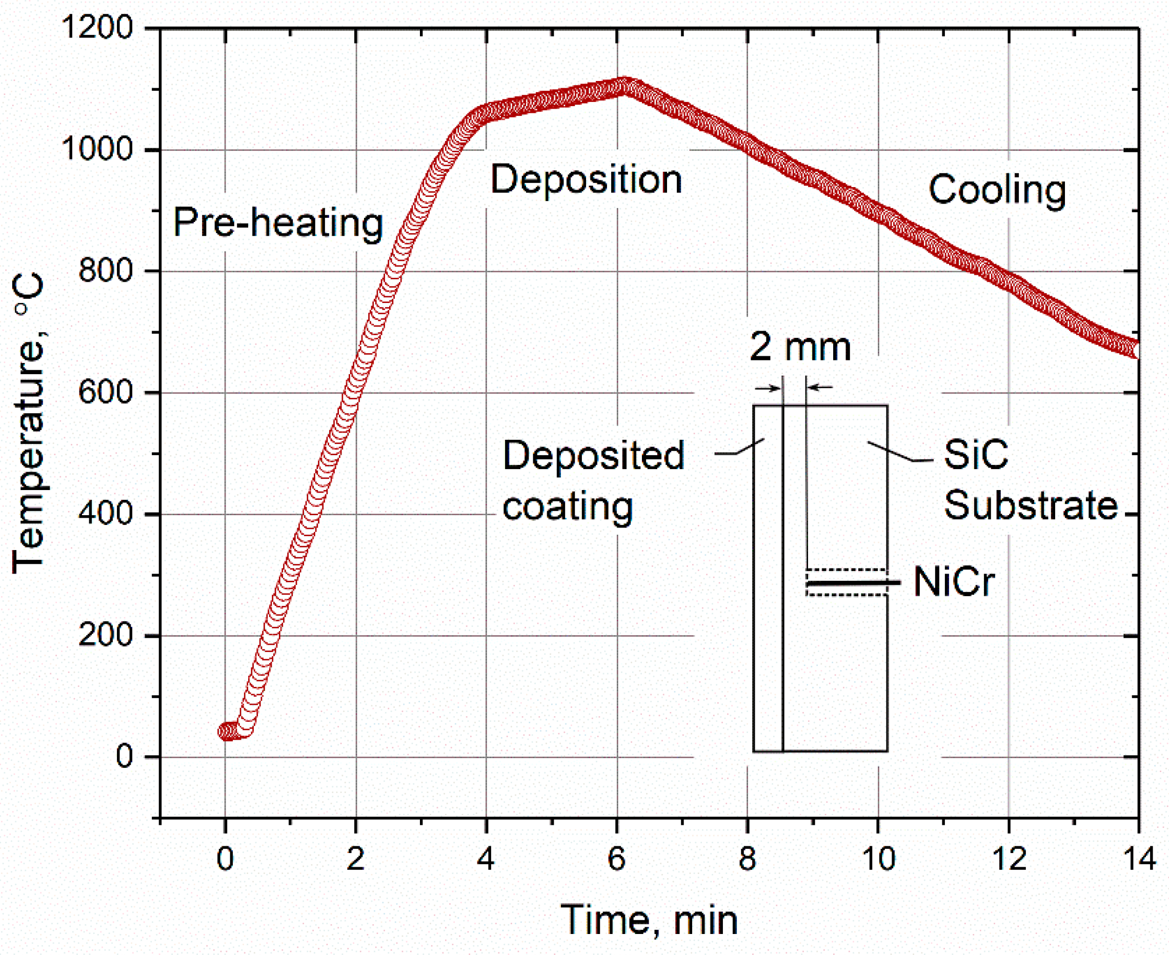
7 particles, which were collected in water and dried subsequently at 70 °C, the crystallization temperature of the material was found to be above 1000 °C, which explains the amorphous structure of the coating deposited at about 550 °C. Aiming at a higher substrate temperature as well as slower cooling rates in order to provide higher energy and longer time for the atoms to rearrange into the crystalline state, VLPPS experiments were conducted in the controlled atmosphere chamber (2 mbar). It was found that it is possible to reach substrate temperatures higher than 1000 °C (
Figure 13) owing to higher plasma power of the O3CP torch as well as to retain it till the deposition starts due to reduced heat transfer under vacuum. To prolong the high-temperature phase after deposition for some minutes, the coating was kept to be heated using the plasma plume and by this procedure, highly crystalline coatings could be produced as shown in
Figure 12a. Nevertheless, it should be mentioned that Si-evaporation remains a problem as more than 10 wt.% Yb
2SiO
5 was detected in the VLPPS coatings.
The HVOF process yields lower flame temperatures in comparison with the plasma spray processes as the flame is generated by combustion. As a result of that, particle temperatures as well as the deposition temperature are lower. Nonetheless, using the HVOF process, Yb
2Si
2O
7 coatings with higher crystallinity in comparison with the APS could be manufactured because of the deposition of un-melted or partially molten particles. This was avoided in the plasma spray processes as un-melted particles increase the porosity levels in the coatings due to imperfect contact regions as well as the porous morphology of the particle itself. In the HVOF process, however, not the porosity stemming from the particle morphology, but the porosity caused by the bad contact can be minimized thanks to very high flame velocity and, thus, the high momentum transfer to the particles in the flame. If the brittle oxide particles are completely un-melted, they break upon high-velocity impact on the substrate, however, if only their core is un-melted and the outer surface is molten, they can adhere on the substrate or on the previously deposited layers. To reach such particle conditions, sensitive process optimizations are required in terms of fuel–oxygen stoichiometry, total gas flow, powder feed rate, stand-off distance, and particle size distribution. Details of these investigations can be found elsewhere [
18] and HVOF microstructure will be further discussed in the following. Consequently, these coatings own higher crystallinity regardless of the lower deposition temperature in the process as un-melted part of the particles remain crystalline. An added benefit of low flame temperature is diminished Si-evaporation from the particles during spraying. It can be seen from
Figure 12a that the detected Yb
2SiO
5 content from about 50 wt.% crystalline HVOF coating is about 5 wt.% which fits well to the feedstock composition although of course the large amorphous content has to be considered.
The microstructure of the coatings sprayed from Yb
2Si
2O
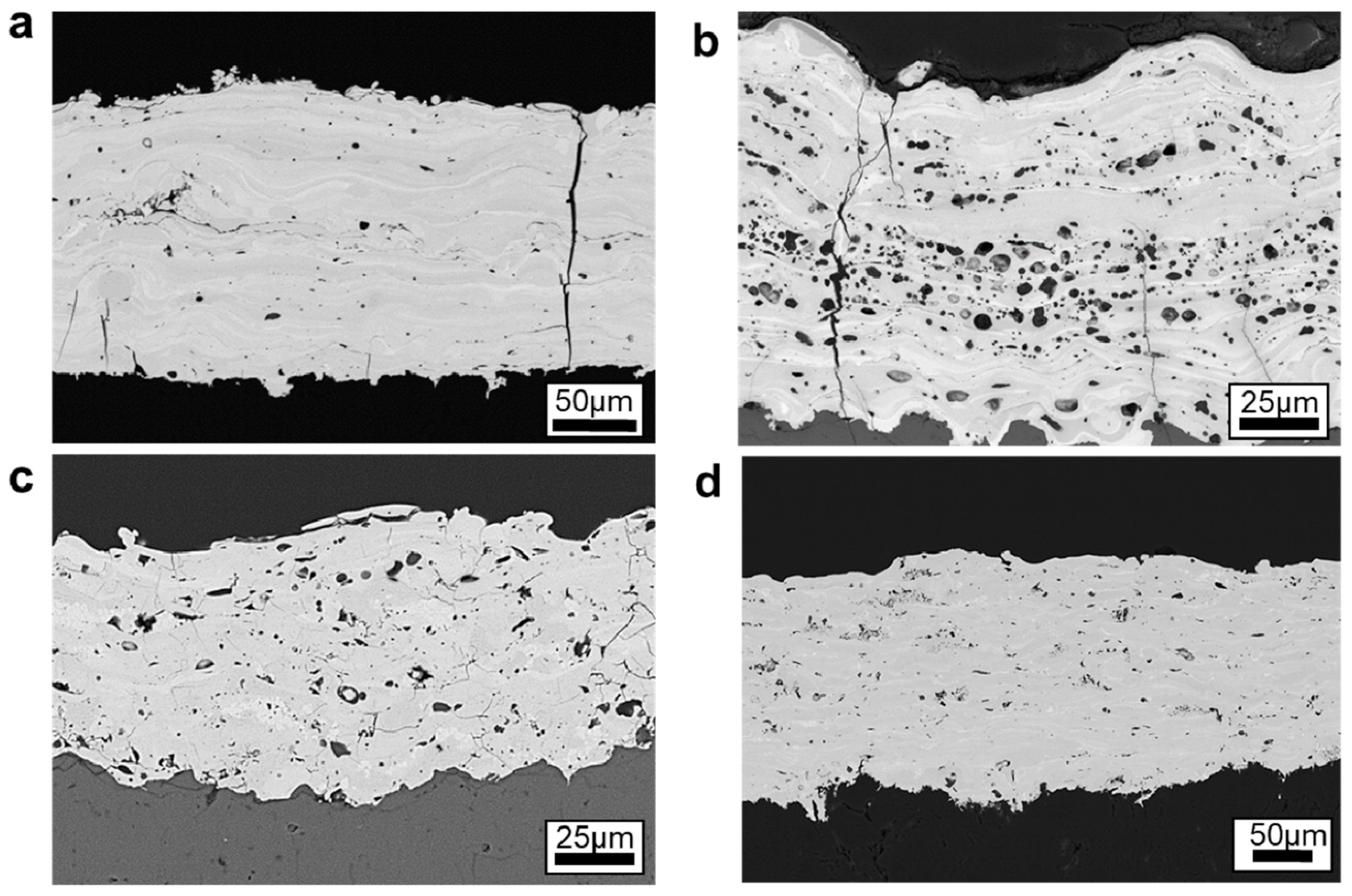
7 feedstock with APS, HVOF and VLPPS processes can be seen in
Figure 14. The two APS coatings (a,b) that were deposited at different temperatures (
Figure 14a is the “standard” APS sample and b is deposited at a higher temperature, further details are discussed below) have vertical cracks running through the thickness of the coatings which is associated with the higher thermal stresses in these coatings due to the significant amount of Yb
2SiO
5 content (about 30 wt.% in these coatings determined after crystallization heat treatment). Because thermal expansion coefficient of Yb
2SiO
5 (7.5 × 10
−6 °C
−1) is larger than that of the Yb
2Si
2O
7 (4.7 × 10
−6 °C
−1) as well as the SiC/SiC substrate (5.1 × 10
−6 °C
−1) [
37]. This leads to greater tensile thermal stresses in the oxide coating after cooling, along with the tensile quenching stresses, which induce the vertical cracking. The high amorphous content in the APS layer would even further increase the CTE mismatch, however simultaneously due to a reduced Young´s modulus of the amorphous state, the effect on the stress level might be limited. Therefore, as cracks are not desired in the EBC microstructure, it is of crucial importance to minimize Si- evaporation during spraying.
Both APS coatings (
Figure 14a,b) were sprayed at similar conditions but sample size in (b) was very small (3 × 3.8 × 36 mm
3) and as a result of that a maximum deposition temperature of about 900 °C could be reached for this particular sample. Therefore, in contrast to standard size APS sample that was analysed in the preceding section and shown in
Figure 14a, the APS coating shown in
Figure 14b is highly crystalline (76 wt.%). The porosity content of the two APS coatings are also dissimilar, i.e., the coating (a) is significantly denser than the coating (b). This difference between the microstructures was associated with the higher crystallinity in the coating (b). Seemingly, heterogeneous nucleation takes place at the splat boundaries during cooling while the centre of the splats remains amorphous. As density increases in the crystallizing zone, the volume is reduced which induces elastic tensile stresses within the amorphous region. Pores within the splat, therefore, nucleate when these stresses are large enough. Other relevant theories to the formation of pores are discussed elsewhere [
20].
No vertical cracking was observed in the fairly dense HVOF layer (
Figure 14c), presumably due to lower Yb
2SiO
5 content and hence reduced thermal stresses in the process as a result of the lower particle and deposition temperatures, respectively. However, isothermal thermal cycling experiments revealed that the adhesion of the HVOF oxide layer on the Si bond coat is poor because the HVOF layer partially delaminated only after few cycles [
18]. The short lifetime of the layer was attributed to the presence of un-melted particles at the interface wherein the cracks can easily propagate. The un-melted particles can be avoided for instance by decreasing the particle size of the feedstock but that means higher amorphous content and Yb
2SiO
5 phase in the layer at the same time.
Figure 14d shows the microstructure of a VLPPS layer that is free of vertical cracks, dense and also crystalline in the as-sprayed state, which makes it a very promising method developed for EBC manufacturing in Jülich. High deposition temperatures (min. 1000 °C) and moderate cooling rates (approx. 55 K/min) in the process as shown in
Figure 13 evidently helps for crystallization as well as for stress relaxation in the layer. Further investigations are ongoing in this direction to understand the effect of deposition temperature and cooling rates on crystallization kinetics and related mechanical properties in the layer, as well as the stress state in the EBC system.
While a variety of coating morphologies can be obtained with thermal spray processes, characteristics of the coatings, typically the size of microstructural features, is controlled by the used feedstock [
38]. For example, the size of intersplat pores is directly depending on the size and shape of powdery feedstocks. Since a well flowable powder in the size range of about 10–100 μm is usually applied for conventional plasma spraying, there is a minimum size for application of powdery feedstock. Suspension plasma spray would be one of alternative processes for conventional ones in this context. Suspension plasma spraying is one of the rather new thermal spray techniques, which has a liquid feed stock and relatively higher plasma power compared with conventional ones. Especially, SPS could supply a great diversity in microstructural features from columnar and porous to bulk-like dense ones [
39,
40]. Main processing parameters, such as gun power, spraying distance, roughness, and particle size distribution in suspension, would play an important role in controlling the microstructures fabricated by SPS.
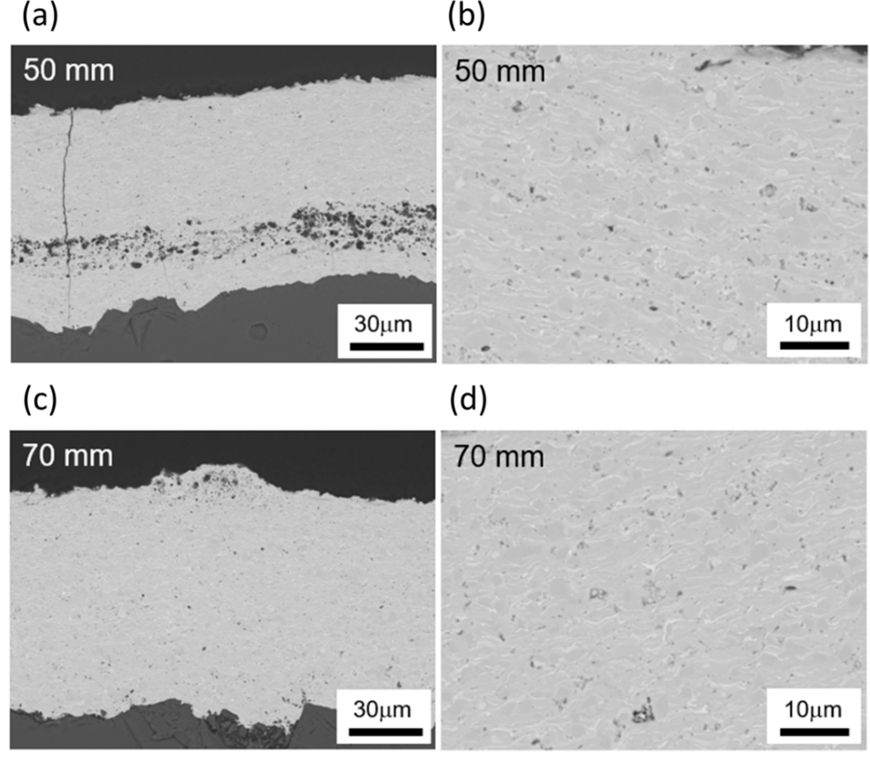
Figure 15 shows the cross-sectional microstructures of Yb
2Si
2O
7 coatings fabricated by using the SPS technique with different spraying distances of 50 and 70 mm. As seen especially in the higher magnification images, bulk-like dense microstructure can be obtained within this work regarding gun power, spraying distance and particle size distribution in suspension feedstock. Vertical cracks in the coating microstructure were inevitable because of tensile stress from rapid cooling after spraying as can be seen in
Figure 15c.
Figure 16 reveals how the stand-off distance influences the substrate temperature and by that e.g., the degree of crystallization. Shorter stand-off distances give higher temperatures and by that also better splat bonding and reduced relaxation, which give a higher segmentation crack density.
Figure 17 shows the X-ray diffraction patterns of Yb
2Si
2O
7 coatings fabricated by using the SPS technique with different spraying distance. Considerable amounts of the amorphous phase were observed from EBC with long spraying distance (90 mm). In the case of short spraying distance (50 mm), the degree of crystallinity was around 80%, which was calculated from the areal intensity ratio between crystalline peaks and amorphous humps of XRD.
