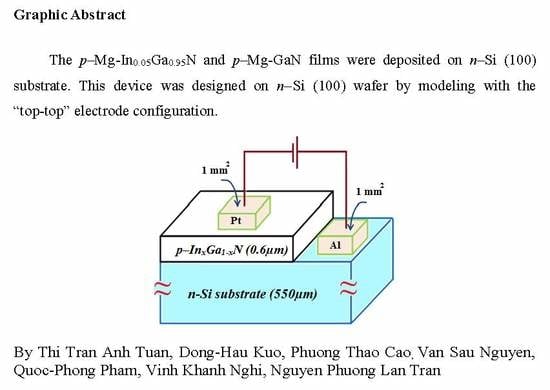
Electrical Characterization of RF Reactive Sputtered p–Mg-InxGa1−xN/n–Si Hetero-Junction Diodes without Using Buffer Layer

 , ,
, ,
Abstract
1. Introduction
2. Materials and Methods
3. Results and Discussion
3.1. Structural and Electrical Characteristics
3.2. The Energy Band Diagram
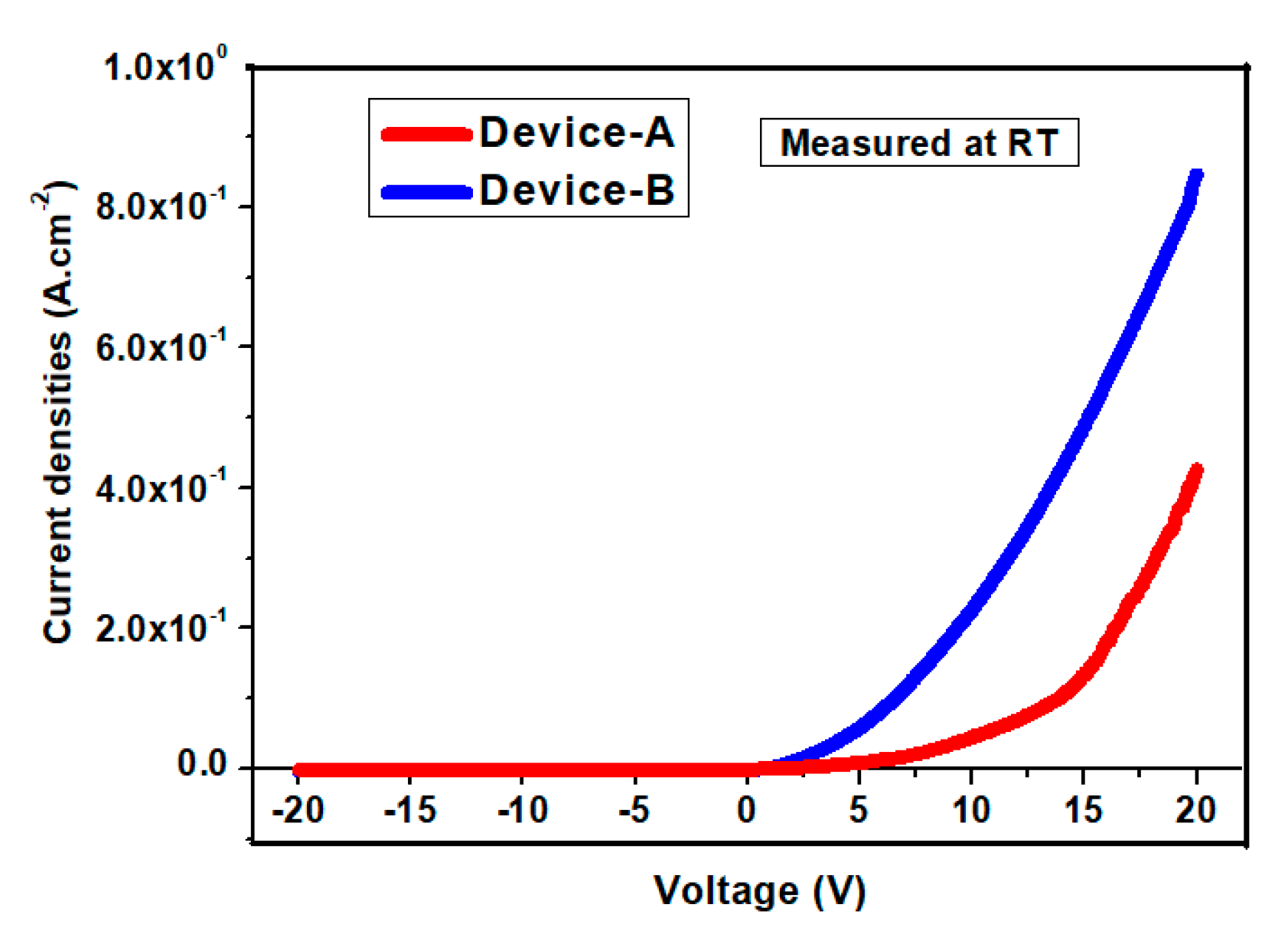
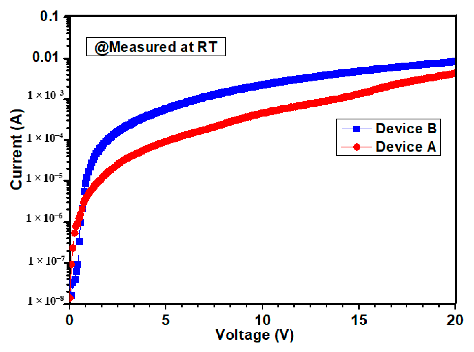
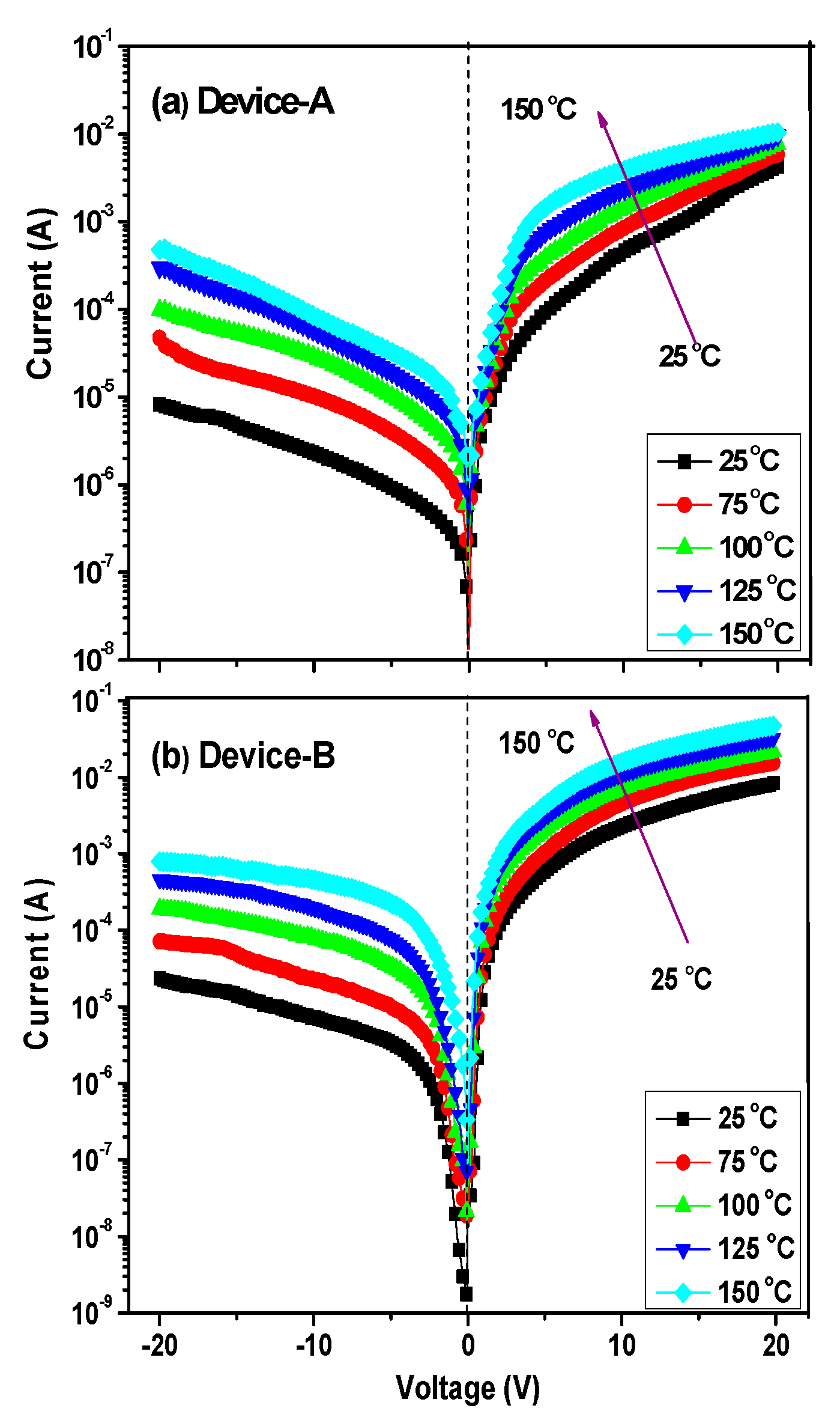
3.3. I–V Measurements
4. Discussion
5. Conclusions
Author Contributions
Funding
Conflicts of Interest
References
- Baik, K.H.; Irokawa, Y.; Ren, F.; Pearton, S.J.; Park, S.S.; Park, S.J. Temperature dependence of forward current characteristics of GaN junction and Schottky rectifiers. Solid State Electron. 2003, 47, 1533–1538. [Google Scholar] [CrossRef]
- Jang, J.S.; Kim, D.; Seong, T.Y. Schottky barrier characteristics of Pt contacts to n-type InGaN. J. Appl. Phys. 2006, 99, 073704. [Google Scholar] [CrossRef]
- Reddy, V.R.; Prasanna, B.P.; Padma, R. Electrical Properties of Rapidly Annealed Ir and Ir/Au Schottky Contacts on n-Type InGaN. J. Metall. 2012, 1, 1–9. [Google Scholar] [CrossRef]
- Cao, X.A.; Lachode, J.R.; Ren, F. Implanted p–n junction in GaN. Solid State Electron. 1999, 43, 1235–1238. [Google Scholar] [CrossRef]
- Hickman, R.; Vanhove, J.M.; Chow, P.P.; Klaassen, J.J. GaN PN junction issues and developments. Solid State Electron. 2000, 44, 377–381. [Google Scholar] [CrossRef]
- Tuan, T.T.A.; Kuo, D.H.; Albert, D.S.; Li, G.Z. Electrical properties of RF-sputtered Zn-doped GaN films and p-Zn-GaN/n -Si hetero junction diode with low leakage current of 10−9 A and a high rectification ratio above 105. Mater. Sci. Eng. B 2017, 222, 18–25. [Google Scholar] [CrossRef]
- Islam, M.R.; Sugita, K.; Horie, M.; Islam, A.Y. Mg doping behavior of MOVPE InxGa1−xN (x~0.4). J.Cryst. Growth 2009, 311, 2817–2820. [Google Scholar] [CrossRef]
- Yohannes, K.; Kuo, D.H. Growth of p-type Cu-doped GaN films with magnetron sputtering at and below 400 °C. Mater. Sci. Semicond. Process. 2015, 29, 288–293. [Google Scholar]
- Ager, J.W.; Miller, N.; Jones, R.E. Mg-doped InN and InGaN Photoluminescence, Capacitance–Voltage and thermo-power measurements. Phys. Status Solidi 2008, 245, 873–877. [Google Scholar] [CrossRef]
- Kuo, D.H.; Li, C.C.; Tuan, T.T.A.; Yen, C.L. Effects of Mg Doping on the Performance of InGaN Films Made by Reactive Sputtering. J. Electron. Mater. 2014, 44, 210–216. [Google Scholar] [CrossRef]
- Tuan, T.T.A.; Kuo, D.H.; Li, C.C.; Li, G.Z. Effect of temperature dependence on electrical characterization of p-n GaN diode fabricated by RF magnetron sputtering. Mater. Sci. Appl. 2015, 6, 809–817. [Google Scholar]
- Tuan, T.T.A.; Kuo, D.H.; Li, C.C.; Yen, W.L. Electrical and structural properties of Mg-doped InxGa1−xN (x ≤ 0.1) and p-InGaN/n-GaN junction diode made all by RF reactive sputtering. Mater. Sci. Eng. B 2015, 193, 13–19. [Google Scholar]
- Tuan, T.T.A.; Kuo, D.H.; Li, C.C.; Yen, W.L. Schottky barrier characteristics of Pt contacts to all sputtering-made n-type GaN and MOS diodes. Mater. Sci. Mater. Electron. 2014, 25, 3264–3270. [Google Scholar] [CrossRef]
- Oh, M.; Lee, J.J.; Lee, L.K.; Oh, H.K. Electrical characteristics of Mg-doped p-GaN treated with the electrochemical potentiostatic activation method. J. Alloy Compd. 2014, 585, 414–417. [Google Scholar] [CrossRef]
- Umeno, M.; Egawa, T.; Ishikawa., H. GaN-based optoelectronic devices on sapphire and Si substrates. Mater. Sci. Semicond. Process. 2001, 4, 459–466. [Google Scholar] [CrossRef]
- Liou, B.W. Design and fabrication of InxGa1−xN/GaN solar cells with a multiple-quantum-well structure on SiCN/Si(111) substrates. Thin Solid Films 2011, 520, 1084–1090. [Google Scholar] [CrossRef]
- Lee, S.Y.; Kim, T.H.; Suh, D.I.; Park, J.E. An electrical characterization of a hetero-junction nanowire (NW) PN diode (n-GaN NW/pSi) formed by dielectrophoresis alignment. Phys. E 2007, 36, 194–198. [Google Scholar] [CrossRef]
- Zebbar, N.; Kheireddine, Y.; Mokeddema, K.; Hafdallah, A.; Kechouanea, M.; Aida, M.S. Structural optical and electrical properties of n-ZnO/p-Si heterojunction prepared by ultrasonic spray. Mater. Sci. Semicond. Process. 2011, 14, 229–234. [Google Scholar] [CrossRef]
- Gad, A.E.; Hoffmann, M.W.G.; Hernandez, R.F. Coaxial p-Si/n-ZnO nanowire heterostructures for energy and sensing applications. Mater. Chem. Phys. 2012, 135, 618–622. [Google Scholar] [CrossRef]
- Tuan, T.T.A.; Kuo, D.H.; Lin, K.; Li, G.Z. Temperature dependence of electrical characteristics of n-InxGa1−xN/p-Si hetero-junctions made totally by RF magnetron sputtering. Thin Solid Films 2015, 589, 182–187. [Google Scholar] [CrossRef]
- Li, C.C.; Kuo, D.H. Material and technology developments of the totally sputtering-made p/n GaN diodes for cost-effective power electronics. Mater. Sci. Mater. Electron. 2014, 25, 1942–1948. [Google Scholar] [CrossRef]
- Kabra, V.; Aamir, L.; Malik, M. Low cost, p-ZnO/n-Si, rectifying nano heterojunction diode: Fabrication and electrical characterization. Beilstein J. Nanotechnol. 2014, 5, 2216–2221. [Google Scholar] [CrossRef] [PubMed]
- Mohd, M.Z.; Baharin, A.; Hassan, Z.; Abu, H.; Abdullah, M.J. MBE growth of GaN pn-junction photodetector on AlN/Si substrate with Ni/Ag as Ohmic contact. Superlattices Microstruct. 2013, 56, 35–44. [Google Scholar] [CrossRef]
- Cho, S.G.; Nahm, T.U.; Kim, E.K. Deep level states and negative photoconductivity in n-ZnO/p-Si hetero-junction diodes. Appl. Phys. 2014, 14, 223–226. [Google Scholar] [CrossRef]
- Wagner, J.; A. Ramakrishnan, A.; Behr, D.; Maier, M. Composition dependence of the band gap energy of InxGa1−xN layers on GaN (x ≤ 0.15) grown by metal-organic chemical vapor deposition. MRS. Internet. J. Nitri. Semi. Res. 1999, 4, 106–111. [Google Scholar] [CrossRef]
- Bedia, F.Z.; Bedia, A.; Benyoucef, B.; Hamzaoui, S. Electrical characterization of n-ZnO/p-Si heterojunction prepared by spray pyrolysis technique. Phys. Procedia 2014, 55, 61–67. [Google Scholar] [CrossRef][Green Version]
- Baydogan, N.; Karacasu, O.; Cimenoglu, H. Effect of annealing temperature on ZnO:Al/p-Si heterojunctions. Thin Solid Films 2012, 520, 5790–5796. [Google Scholar] [CrossRef]
- Li, J.L.; Schubert, E.F.; Graff, J.W.; Osinsky, A.; Schaff, W.F. Low-resistance ohmic contacts to p-type GaN. Appl. Phys. Lett. 2000, 76, 2728–2730. [Google Scholar] [CrossRef]
- Ponce, A.R.; Olguín, D.; Calderón, H.I. Calculation of the effective masses of II-VI semiconductor compounds. Superficies y Vacío 2003, 16, 26–28. [Google Scholar]
- Suzuki, M.; Uenoyama, T. First-Principles Calculation of Effective Mass Parameters of Gallium Nitride. Jpn. J. Appl. Phys. 1995, 34, 3442–3446. [Google Scholar] [CrossRef]
- Crowell, C.R. The richardson constant for thermionic Emission in schottky barrier diodes. Solid State Electron. 1965, 8, 395–399. [Google Scholar] [CrossRef]
- Kumar, A.; Vinayak, S.; Singh, R. Micro-structural and temperature dependent electrical characterization of Ni/GaN Schottky barrier diodes. Curr. Appl. Phys. 2013, 13, 1137–1142. [Google Scholar] [CrossRef]
- Cheung, S.K.; Cheung, N.W. Extraction of Schottky diode parameters from forward current-voltage characteristics. Appl. Phys. Lett. 1986, 49, 85–87. [Google Scholar] [CrossRef]
- Benamara, Z.; Akkal, B.; Talbi, A.; Gruzza, B. Electrical transport characteristics of Au/n-GaN Schottky diodes. Mater. Sci. Eng. C 2006, 26, 519–522. [Google Scholar] [CrossRef]
- Tuan, T.T.A.; Kuo, D.H. Characteristics of RF reactive sputter-deposited Pt/SiO2/n-InGaN MOS Schottky diodes. Mater. Sci. Semicond. Process. 2015, 30, 314–320. [Google Scholar] [CrossRef]
- Norde, H. A modified forward I-V plot for Schottky diodes with high series resistance. J. Appl. Phys. 1979, 50, 5052–5505. [Google Scholar] [CrossRef]
- Urgessa, Z.N.; Dobson, S.R.; Talla, K.; Murape, D.M. Optical and electrical characteristics of ZnO/Si heterojunction. Phys. B 2014, 439, 149–152. [Google Scholar] [CrossRef]
- Keskenler, E.F.; Tomakina, M.; Dogan, S. Growth and characterization of Ag/n-ZnO/p-Si/Al heterojunction diode by sol–gel spin technique. J. Alloy Compd. 2013, 550, 129–132. [Google Scholar] [CrossRef]
- Chirakkara, S.; Krupanidhi, S.B. Study of n-ZnO/p-Si (100) thin film heterojunctions by pulsed laser deposition without buffer layer. Thin Solid Films 2012, 520, 5894–5899. [Google Scholar] [CrossRef]
- Shen, Y.; Chen, X.; Yan, X.S. Low-voltage blue light emission from n-ZnO/p-GaN heterojunction formed by RF magnetron sputtering method. Curr. Appl. Phys. 2014, 14, 345–348. [Google Scholar] [CrossRef]
- Hsueh, K.P. Temperature dependent current–voltage characteristics of n-MgxZn1−xO/p-GaN junction diodes. Microelectron. Eng. 2011, 88, 1016–1018. [Google Scholar] [CrossRef]


| Temp (°C) | Leakage Current (A) at −5 V | Barrier Height | From I–V | Cheung’s Function dV/dln(I) versus I | ||
|---|---|---|---|---|---|---|
| I–V | Norde | n | Rs (Ω) | n | ||
| Device-A | ||||||
| 25 | 9.31 × 10⁻⁷ | 0.54 | 0.56 | 5.9 | 876 | 6.4 |
| 75 | 4.02 × 10⁻⁶ | 0.57 | 0.58 | 5.6 | 683 | 5.8 |
| 100 | 1.03 × 10⁻⁵ | 0.63 | 0.64 | 5.4 | 549 | 5.5 |
| 125 | 1.91 × 10⁻⁵ | 0.66 | 0.68 | 5.0 | 467 | 5.3 |
| 150 | 3.26 × 10⁻⁵ | 0.69 | 0.71 | 4.8 | 413 | 5.1 |
| Device-B | ||||||
| 25 | 3.38 × 10⁻⁶ | 0.50 | 0.53 | 5.1 | 486 | 5.3 |
| 75 | 9.92 × 10⁻⁵ | 0.53 | 0.55 | 4.8 | 292 | 4.9 |
| 100 | 3.43 × 10⁻⁵ | 0.57 | 0.60 | 4.6 | 233 | 4.7 |
| 125 | 7.81 × 10⁻⁵ | 0.60 | 0.62 | 4.1 | 173 | 4.2 |
| 150 | 2.64 × 10⁻⁴ | 0.62 | 0.64 | 3.6 | 133 | 3.8 |
© 2019 by the authors. Licensee MDPI, Basel, Switzerland. This article is an open access article distributed under the terms and conditions of the Creative Commons Attribution (CC BY) license (http://creativecommons.org/licenses/by/4.0/).
Share and Cite
Tuan, T.T.A.; Kuo, D.-H.; Cao, P.T.; Nguyen, V.S.; Pham, Q.-P.; Nghi, V.K.; Tran, N.P.L. Electrical Characterization of RF Reactive Sputtered p–Mg-InxGa1−xN/n–Si Hetero-Junction Diodes without Using Buffer Layer. Coatings 2019, 9, 699. https://doi.org/10.3390/coatings9110699
Tuan TTA, Kuo D-H, Cao PT, Nguyen VS, Pham Q-P, Nghi VK, Tran NPL. Electrical Characterization of RF Reactive Sputtered p–Mg-InxGa1−xN/n–Si Hetero-Junction Diodes without Using Buffer Layer. Coatings. 2019; 9(11):699. https://doi.org/10.3390/coatings9110699
Chicago/Turabian StyleTuan, Thi Tran Anh, Dong-Hau Kuo, Phuong Thao Cao, Van Sau Nguyen, Quoc-Phong Pham, Vinh Khanh Nghi, and Nguyen Phuong Lan Tran. 2019. "Electrical Characterization of RF Reactive Sputtered p–Mg-InxGa1−xN/n–Si Hetero-Junction Diodes without Using Buffer Layer" Coatings 9, no. 11: 699. https://doi.org/10.3390/coatings9110699
APA StyleTuan, T. T. A., Kuo, D.-H., Cao, P. T., Nguyen, V. S., Pham, Q.-P., Nghi, V. K., & Tran, N. P. L. (2019). Electrical Characterization of RF Reactive Sputtered p–Mg-InxGa1−xN/n–Si Hetero-Junction Diodes without Using Buffer Layer. Coatings, 9(11), 699. https://doi.org/10.3390/coatings9110699