Article

Preparation of Micro-Patterned CaMn7O12 Ceramic Films via a Photosensitive Sol-Gel Method

1
School of Materials Science and Engineering, Xi’an University of Technology, Xi’an 710048, China
2
School of Biological and Chemical Engineering, Panzhihua University, Panzhihua 617000, China
3
College of Vanadium and Titanium, Panzhihua University, Panzhihua 617000, China
*
Authors to whom correspondence should be addressed.
Coatings 2019, 9(10), 650; https://doi.org/10.3390/coatings9100650
Submission received: 24 August 2019 / Revised: 30 September 2019 / Accepted: 8 October 2019 / Published: 9 October 2019

Abstract

:
Mn/acetylacetone chelate was synthesized using Mn(CH3COO)2·4H2O as raw material, methanol as the solvent, and acetylacetone as the chelating agent. The ultraviolet (UV)-absorption peak of the synthesized chelate was found around 298 nm. CaMn7O12 sol was subsequently prepared using the Mn/AcAc chelate as the Mn source and calcium nitrate as the calcium source. The UV test indicates that the CaMn7O12 sol has the UV-sensitive characteristics. Owing to its photo-sensitivity, micro-patterned CaMn7O12 ceramic film can be prepared without photoresist, only through dip-coating, drying, UV-irradiation, solvent-washing, and heat treatment. The magnetic test result indicates that the micro-patterned CaMn7O12 ceramic film has a saturation magnetization of 112.8 emu/cm3, which is close to that of non-patterned CaMn7O12 ceramic film.

1. Introduction

A multiferroic material refers to a material that simultaneously has a ferroic order of two or more, such as ferroelectric (reverse), ferromagnetic (reverse), or ferroelastic sequences [1,2,3,4,5]. As the second type of single-phase multiferroic material, CaMn7O12 has ferroelectric properties caused by its special helical magnetic structure, and produces a strong magneto-electric coupling effect. Therefore, CaMn7O12 has potential applications in spin electronics, multi-state storage devices, and microelectromechanical system (MEMS) [6,7,8,9,10,11,12]. In recent years, while there have been more studies on the structure and performance of bulk CaMn7O12 (including single crystals and polycrystalline samples), there have been few studies on CaMn7O12 film [13,14,15,16,17,18]. In 2015, Huon et al. deposited c-axis oriented CaMn7O12 film. Subsequently, they studied the helical magnetic ordering structure of the Sr-doped CaMn7O12 film [19,20,21]. In 2018, our group adopted sol-gel technology to prepare a CaMn7O12 ceramic film with good bi-axial texture on a LaAlO3 (LAO) substrate; the work confirmed that the saturation magnetization of the CaMn7O12 ceramic film was better than that of the bulk material [22].
Micro-patterning is required when applying single-phase multiferroic CaMn7O12 to the microelectronics field. The traditional photoresist etching process includes preparing film, coating photoresist, ultraviolet (UV) exposure, leaching, photoresist removal, etc. [23]. However, it has a few disadvantages such as requiring expensive processing equipment, the complex process, time-consuming, and ion damage. Furthermore, expensive photoresist is essential for transferring a geometric pattern structure from a mask to films [24,25]. UV-photosensitive sol-gel technology is a new technology that can be applied to the micro-fabrication for film. In the preparation of sols some chemical modifier was added in the sol precursor, and it can coordinate with some metal ions to form chelating structures. Under the UV irradiation, these structures decompose rapidly resulting in changes the solubility of its gel film in organic solvent. Making use of the different solubility, the micro-pattern consistent with the negative phase of mask can be prepared. As a result, the photosensitive sol-gel method shows many advantages such as large deposition area, simple process, and low process as well [26].
In our previous work, the method was successfully applied for the preparation of micro-patterns on various functional films, such as on ZnO, BiFeO3, YBa2Cu3O7−x, WO3, ZrO–SiO2, and La0.67Sr0.33MnO3 [26,27,28,29,30,31]. In this paper, the UV-photosensitive sol-gel technology was further applied to the preparation of micro-patterned CaMn7O12 ceramic film. Micro-patterned CaMn7O12 ceramic film with a clear profile and a regular structure was facilely obtained. In addition, the magnetic properties of micro-patterned CaMn7O12 ceramic film was characterized with vibrating-sample magnetometer (VSM) and compared with that of the un-patterned one.

2. Experimental

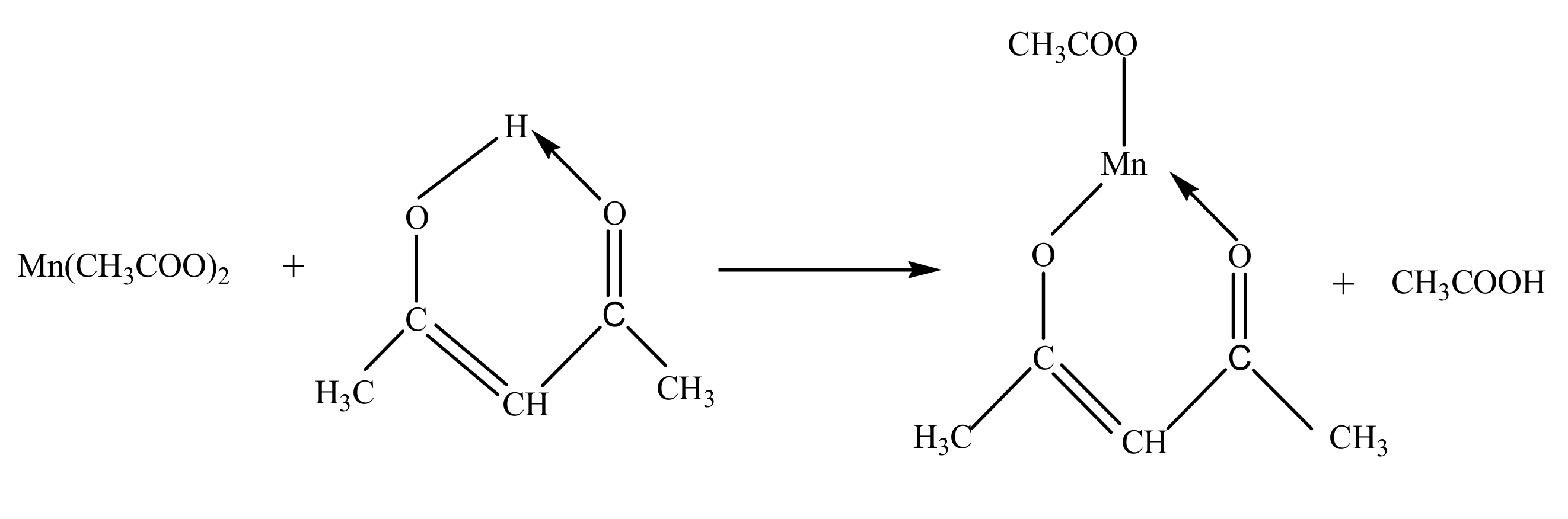
2.1. Preparation of Photosensitive CaMn7O12 Sol

The CaMn7O12 sol was prepared with a metal ion ratio of Ca:Mn = 1:7 in the sol. Ca(NO3)2·4H2O and Mn(CH3COO)2·4H2O were used as raw materials, methanol (MeOH) was used as the solvent, and acetylacetone (AcAc) was used as the chelating agent. First, 0.1771 g of Ca(NO3)2·4H2O (0.75 mmol) was dissolved in 5 mL of anhydrous MeOH to obtain solution A; then, 1.2867 g (5.2 mmol) of Mn(CH3COO)2·4H2O was added to 5 mL of anhydrous MeOH and 0.53 g of AcAc as the chelating agent (5.2 mmol) was further added. After stirring, the mixture became clear and was named solution B. Solutions A and B were mixed and stirred and the total metal ion concentration was adjusted to 0.4 mol/L by changing the amount of MeOH and allowed to stand for 24 h to obtain a stable and uniform CaMn7O12 UV-photosensitive sol.

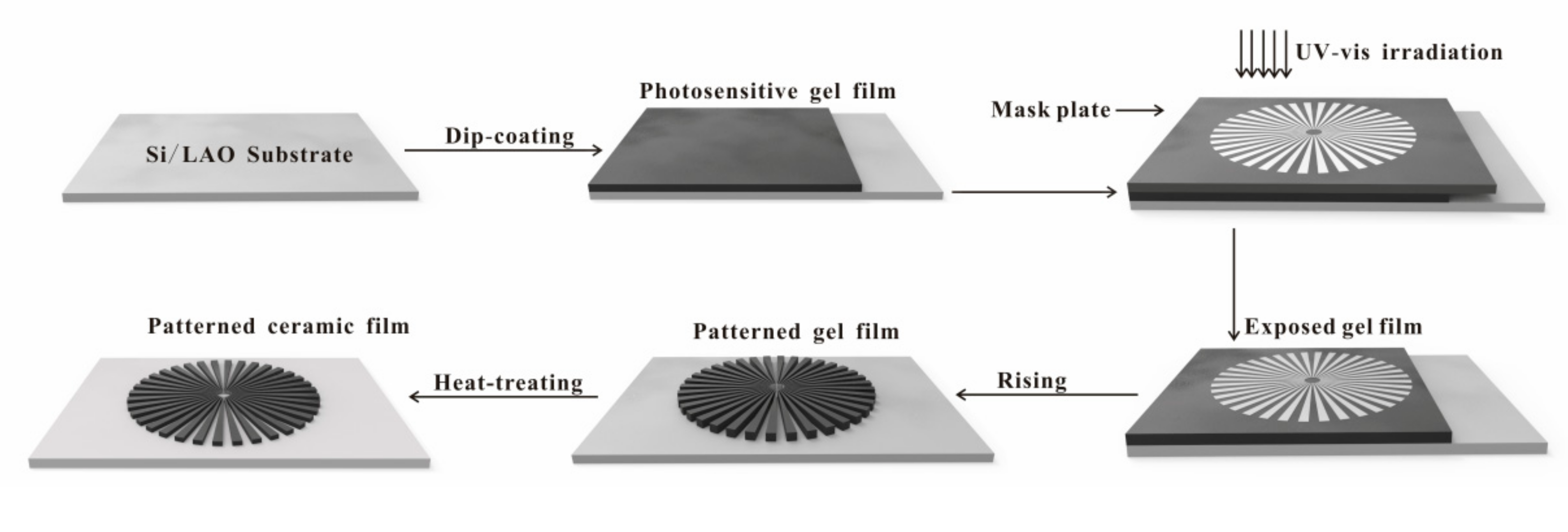
2.2. Preparation of Micro-Patterned CaMn7O12 Ceramic Film

Using LaAlO3 as a substrate, the CaMn7O12 gel film was obtained via dip-coating in a glove box with a humidity <30% R.H. The pulling speed was 2 mm/s and the temperature was 25 °C. The thickness of the obtained CaMn7O12 gel film was 207 nm. The gel film was dried at 80 °C for 10 min, then irradiated in air for 60 min through a mask. Then, the film was washed in a mixed solution of ethanol and n-butanol (molar ratio 10:1) for 15 s to obtain the patterned CaMn7O12 gel film. After that the patterned CaMn7O12 gel film was dried at 350 °C in a heat treatment furnace for 10 min to remove the organic components. Finally, the film was heat treated at 730 °C for 60 min to obtain a crystallized CaMn7O12 ceramic film with a pattern structure. Its thickness was 49 nm. The specific preparation process is also shown in Figure 1.

2.3. Characterizations

Phase and orientation of micro-patterned CaMn7O12 ceramic film with striped structure were analyzed by X-ray diffractometer (XRD) with Cu Kα radiation (7000S, Shimadzu, Kyoto, Japan). The absorption spectrum and photosensitive performance of the as-prepared sol and its gel film were recorded with an Ultraviolet-visible spectrometer (UV-Vis) (V-570, Shimadzu, Kyoto, Japan). Thickness of films was executed by VASE Ellipsometer (VB-400, J.A.Woollam, Lincoln, NE, USA). The chemical composition of the ceramic film was determined by energy dispersive X-ray spectrometry (EDS). An optical microscope (Olympus, BX51, Tokyo, Japan), a laser confocal scanning microscopy (LCSM) (Olympus OLS4000, Tokyo, Japan), and a scanning electron microscope (SEM) (JSM-7000F, JOEL, Tokyo, Japan) were used to observe the surface morphology of the micro-patterned CaMn7O12 ceramic films. The UV exposure process was carried out using the UV light source (USHIO SP-9, Tokyo, Japan), which was a high-pressure mercury lamp (UXM-Q256BY) with a power of 250 W and a main wavelength range from 220 to 375 nm. The distance between the sample and the lamp was 10 cm, and the as-obtained light intensity was 97 mW/cm2. Saturation magnetization and coercivity were performed with a multi-function vibrating sample magnetometer (VSM) in a physical property measurement system (VersaLab, Quantum Design, San Diego, CA, USA).

3. Results and Discussion

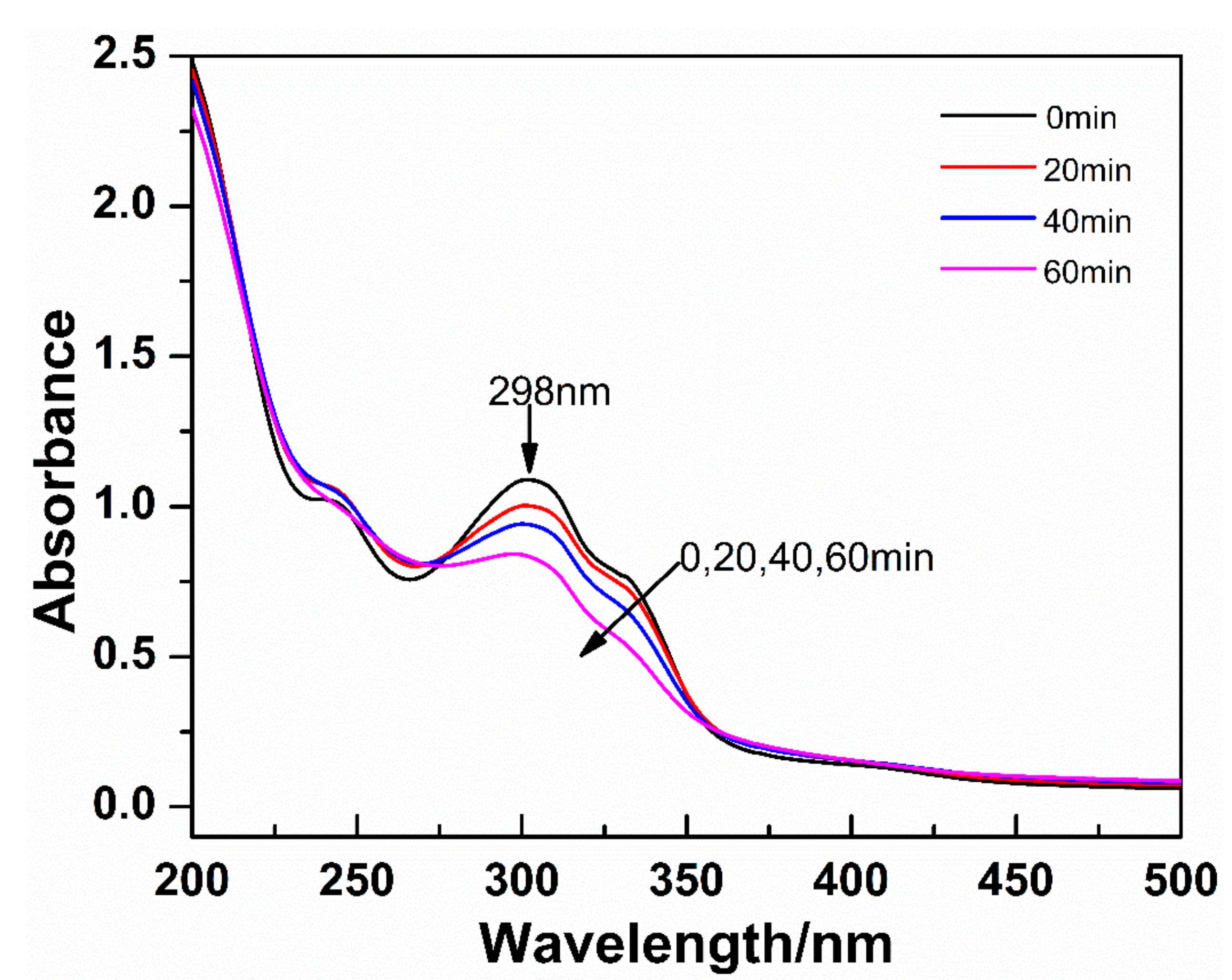
3.1. Photo-Sensitivity of the CaMn7O12 Sol and Its Gel Thin Film

To study the photo-sensitivity of the CaMn7O12 sol and its gel film, the UV spectra of the AcAc and MeOH (AcAc + MeOH) mixture, a solution containing Ca2+ (Ca + AcAc + MeOH), a solution containing Mn2+ (Mn + AcAc + MeOH), and a CaMn7O12 sol were measured and the results are shown in Figure 2. It can be seen that the characteristic UV absorption peak of AcAc-MeOH solution is at 274 nm and the peak is attributed to the π-π* electron transition of the K-adsorption band of the enol structure of AcAc. After adding a Ca2+ into the solution, the characteristic UV adsorption peak was still at 274 nm, indicating that the enol structure of AcAc was still present and Ca2+ does not react with AcAc. After adding the manganese ion into the solution, the characteristic UV adsorption peak occurs at 298 nm. Compared with the adsorption peak of the enol structure of AcAc, there was a red-shift of 24 nm, indicating a chelating reaction between Mn(CH3COO)2·4H2O and AcAc. In the reaction between Mn2+ and AcAc, the acetic group was partially substituted by AcAc through chemical coordination, as shown in Scheme 1. The red-shift of the characteristic UV absorption peak is ascribed to the above reaction. Therefore, the absorption peak at 298 nm corresponds to the π-π* transition of the Mn/AcAc metal-coordinated chelate rings formed between Mn2+ and AcAc [32].
The UV absorption spectrum of the CaMn7O12 precursor sol is also shown in Figure 2. The main characteristic absorption peak at 298 nm is consistent with the absorption peak of Mn/AcAc chelate, which means that the addition of Ca2+ does not cause the destruction of the structure of Mn/AcAc chelate, and the UV absorption of the CaMn7O12 sol is derived from the Mn/AcAc chelate.
The CaMn7O12 gel film was obtained via the dip-coating method, the variation in the UV spectrum of the CaMn7O12 gel film with irradiation time was tested and is shown in Figure 3. The UV absorption spectra of CaMn7O12 gel film around 330 nm became wider compared with that of CaMn7O12 sol, which was related to the different states of chelate molecules in the sol and gel film. In the sol, the chelate molecules exist in a free form. While in the gel film, the chelate molecules exist in a stacked form, then causing intermolecular electron transfer. The migration of electrons leads to the variation of energy levels and band, resulting in the wideness of the UV absorption spectrum of the CaMn7O12 gel film [33,34]. As the irradiation time is prolonged, the characteristic absorption peak that characterizes the chelate content gradually became smaller, indicating that the corresponding coordinated chelate in the gel film was continuously photo-decomposed and the concentration of the coordinated chelate decreases. The reason is that under the irradiation condition of UV lamp, the chelates in CaMn7O12 gel film absorbs UV irradiation with a certain wavelength (λ > 200 nm) and then electron excitation occurs (Scheme 2). As the excited state is unstable, further reactions can take place (Scheme 3). Since a portion of electrons distributes around the oxygen atoms, the electrons excitation can reduce the coordination intensity of AcAc. Therefore, the chelating structures break continuously as the irradiation time prolongs [26]. This chemical structural change of the gel film can significantly change its solubility in organic solvents. Making use of the photo-sensitive characteristics, the gel film was irradiated by UV light through a mask and then washed in organic solvent. During the process, the regions shielded by the mask can be washed away and the regions exposed to the UV light remain intact, resulting in a fine pattern consistent with the negative image of the mask.

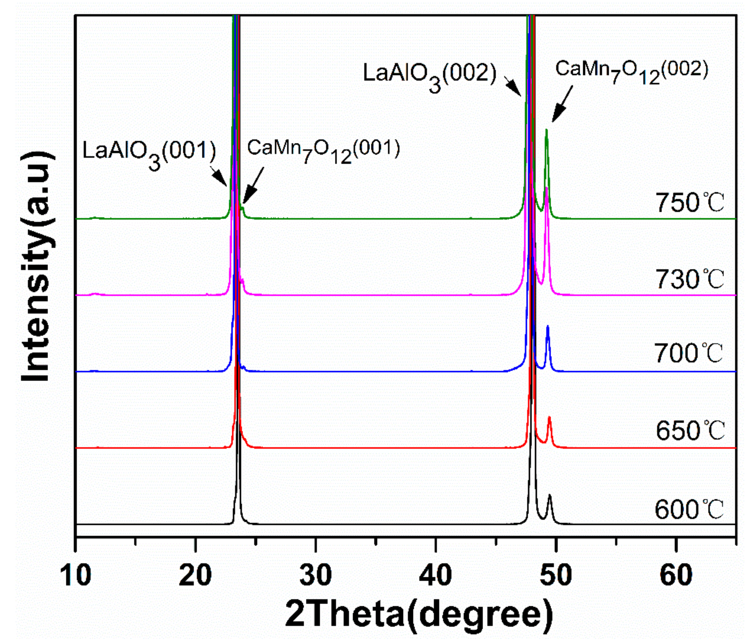
3.2. Phase Composition of Micro-Patterned CaMn7O12 Ceramic Film

In order to further ascertain crystallization process of the micro-patterned CaMn7O12 ceramic film, CaMn7O12 films sintered at different temperatures ranging from 600 to 750 °C were characterized by XRD measurement. As shown in Figure 4, the CaMn7O12 film sintered below 700 °C was incomplete crystallized, because only a weak diffraction peak (2θ = 49.38°) of CaMn7O12 (002) was observed. When the sintering temperature was heated up to 730 °C, another reflection peak at 2θ = 24.09° corresponding to (001) CaMn7O12 phase appeared and no intermediate phase was detected (according to the JCPDF standards, Card No. 26-1114) [19]. In addition, as sintered temperature was raised to 75 °C, diffraction peaks intensity of CaMn7O12 phase had no significant increase. It indicated that the crystallization of CaMn7O12 phase in the CaMn7O12 film had completed at ~730 °C. From the point of view of energy and environmental protection, 730 °C was chosen as the optimum sintered temperature. Compared with LaAlO3 substrate, the diffraction peaks of CaMn7O12 ceramic films were weaker because of their smaller thickness.

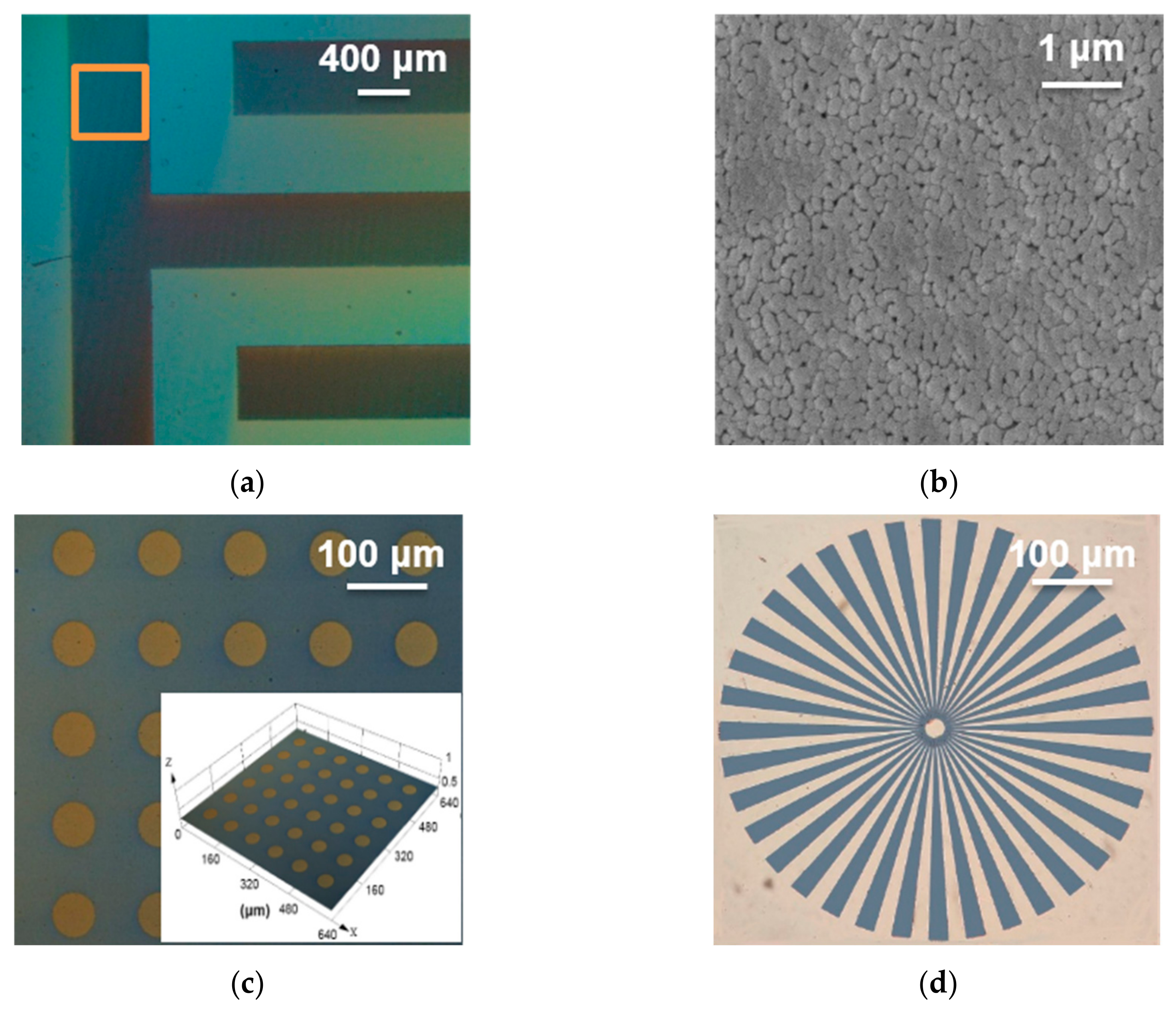
3.3. Micrograph of Micro-Patterned CaMn7O12 Ceramic Film

Micro-patterned CaMn7O12 ceramic films were prepared with masks having stripe, dot-matrix, and radial structures respectively. Figure 5a shows an optical micrograph of the film with strip structure, where the lighter regions are LaAlO3 matrix while the darker regions are CaMn7O12 ceramic film. It can be seen that the pattern on CaMn7O12 ceramic film has a clear profile and a uniform surface. Figure 5b shows SEM photograph of yellow selected area in Figure 5a. It can be seen that the film is compact and crack-free, and the grain size is uniform. The average particle size is about 180 nm, which is close to the particle size of the pristine CaMn7O12 ceramic film prepared in the previous study [22]. Figure 5c shows the laser confocal graphs of the film with dot-matrix (the inset is its 3D graph). The diameter and period of columns in dot-matrix structure are both 50 μm. The pattern is also clear and regular, without cracks or pores. Figure 5d shows the laser confocal graph of the film with radial structure, indicating the minimum line width in the micro-fabrication process can reach 5 μm.

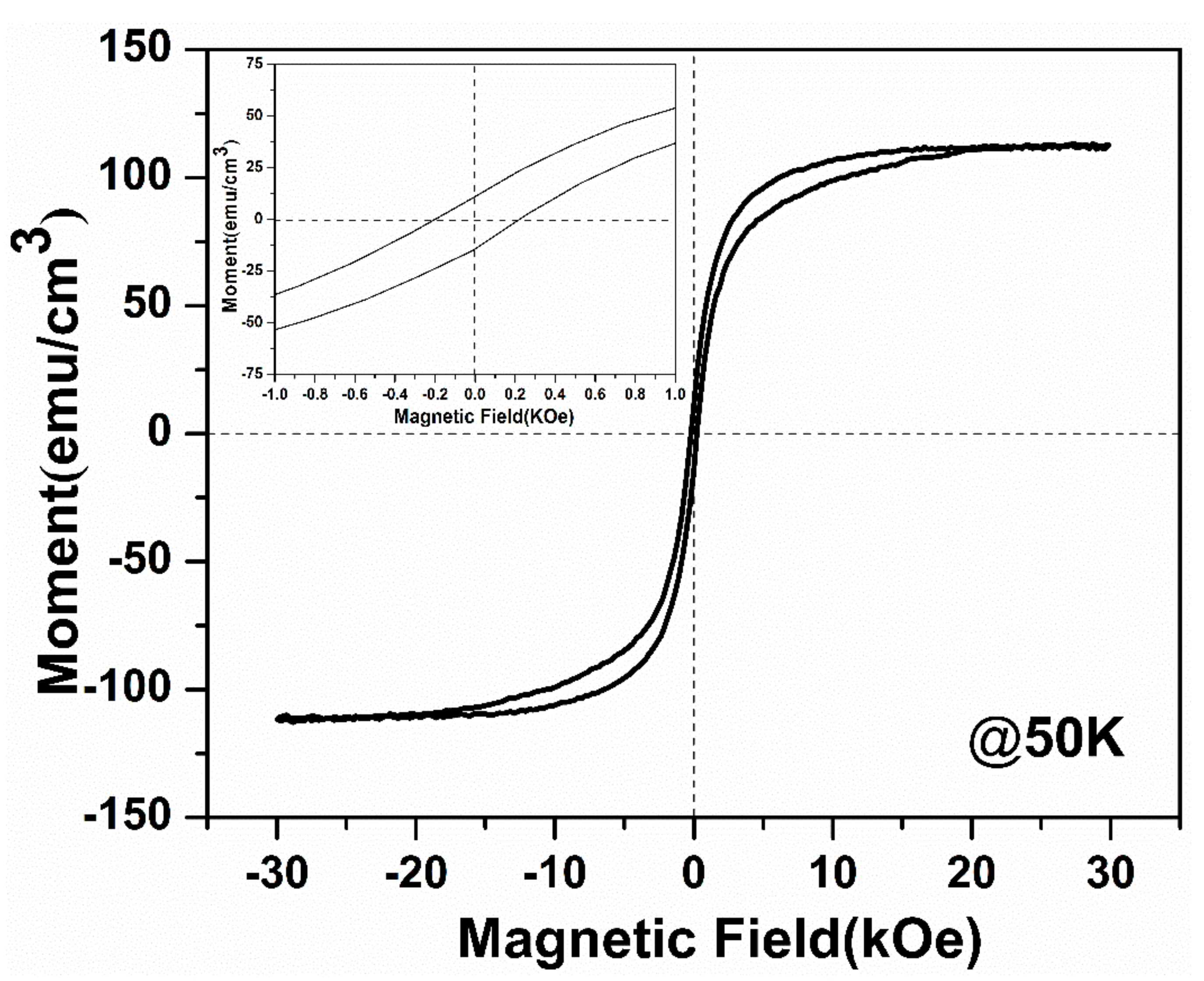
3.4. Magnetic Properties of the Micro-Patterned CaMn7O12 Ceramic Film

The magnetic property of micro-patterned CaMn7O12 ceramic film with dot-matrix structure is shown in Figure 6. It can be seen that the micro-patterned CaMn7O12 ceramic film exhibits apparent anti-ferromagnetic characteristics. The properties include a saturation magnetization (Ms) of 112.8 emu/cm3 and a coercivity (Hc) of 211 Oe, which are close to the saturation magnetization (Ms = 114.2 emu/cm3, Hc = 220 Oe) of the CaMn7O12 ceramic film without patterned structure [22]. The result indicates that the photosensitive sol-gel micro-patterning process does not affect the magnetic properties of the CaMn7O12 film. The magnetic properties of multiferroic films are generally affected by factors such as grain size, grain morphology, grain boundaries, etc. However, for the process of preparing fine patterns by the photosensitive sol-gel method, the micro-patterning process was performed prior to annealing treatment. Consequently, the crystallinity of the film was not affected. As a result, the magnetic properties of pattern ceramic films would not have been affected significantly [30].

4. Conclusions

In the paper, a CaMn7O12 sol with UV sensitivity was prepared using Ca(NO3)2·4H2O and Mn(CH3COO)2·4H2O as the raw materials, MeOH as a solvent, and AcAc as a chemical modifier. The Mn2+ in sol can chelate with AcAc, then form an Mn/AcAc metal-coordinated chelate ring, resulting in an obvious UV-absorption peak at 298 nm. CaMn7O12 gel film was obtained through dip-coating process. After processes including masking, UV-radiation, solvent washing, the micro-patterned CaMn7O12 gel film was obtained. After heat treatment at 730 °C, the micro-patterned CaMn7O12 gel film was converted into the micro-patterned crystalline CaMn7O12 ceramic film. The saturation magnetization at 50 K of the micro-patterned CaMn7O12 ceramic film reached 112.8 emu/cm3, which was close to the performance of the ceramic film without micro-fabrication.

Author Contributions

Designed the research project, G.Z.; performed all experiments, Y.W. and C.W.; characterized samples and analyzed corresponding data, Y.W. and C.W.; wrote the initial draft and provided valuable comments and suggestions to the work, Z.D.

Funding

This work was supported by the project of the National Natural Science Foundation of China (51672212), the Scientific Research Fund (2013JK0676) of the Department of Education and Nature Science Foundation (2018JM5019) of Shaanxi Province, the Fund Project (16ZB0470) of Sichuan Provincial Department of Education, the Invested by the Seed Capital of Panzhihua University Science and Technology Park (2019-12), the Doctoral Fund (bkqj2017009) and Student Innovation and Entrepreneurship Training Project (2019cxcy059) of Panzhihua University.

Conflicts of Interest

The authors declare no conflict of interest.

References

  1. Lu, C.L.; Hu, W.J.; Tian, Y.F.; Wu, T. Multiferroic oxide thin films and heterostructures. Appl. Phys. Rev. 2015, 2, 021304. [Google Scholar] [CrossRef]
  2. Ramesh, R.; Spaldin, N.A. Multiferroics: Progress and prospects in thin films. Nat. Mater. 2007, 6, 21–29. [Google Scholar] [CrossRef] [PubMed]
  3. Fiebig, M. Revival of the magnetoelectric effect. J. Phys. D Appl. Phys. 2005, 38, R1–R30. [Google Scholar] [CrossRef]
  4. Eerenstein, W.; Mathur, N.D.; Scott, J. Multiferroic and magnetoelectric materials. Nature 2006, 44, 759–765. [Google Scholar] [CrossRef] [PubMed]
  5. Spaldin, N.A.; Fiebig, M. The renaissance of magnetoeletric multiferroics. Science 2005, 309, 391–392. [Google Scholar] [CrossRef]
  6. Lu, X.Z.; Whangbo, M.H.; Dong, S.; Gong, X.G.; Xiang, H.J. Giant ferroelectric polarization of CaMn7O12 induced by combined effect of Dzyaloshinskii-Moriya interaction and exchange striction. Phys. Rev. Lett. 2012, 108, 187204. [Google Scholar] [CrossRef] [PubMed]
  7. Johnson, R.D.; Chapon, L.C.; Khalyavin, D.D.; Manuel, P.; Radaelli, P.G.; Martin, C. Giant improper ferroelectricity in the ferroaxial magnet CaMn7O12. Phys. Rev. Lett. 2012, 108, 067201. [Google Scholar] [CrossRef] [PubMed]
  8. Perks, N.J.; Johnson, R.D.; Martin, C.; Chapon, L.C.; Radaelli, P.G. Magneto-orbital helices as a route to route to coupling magnetism and ferroelectricity in multiferroic CaMn7O12. Nat. Commun. 2012, 3, 1277. [Google Scholar] [CrossRef] [PubMed]
  9. Zhang, G.Q.; Dong, S.; Yan, Z.B.; Guo, Y.Y.; Zhang, Q.F.; Yunoki, S.; Dagotto, E.; Liu, J.M. Multiferroic properties of CaMn7O12. Phys. Rev. B 2011, 84, 174413. [Google Scholar] [CrossRef]
  10. Zhang, H.G.; Ma, X.C.; Xie, L. The structural and magnetic properties of Sr-doped multiferroic CaMn7O12. Int. J. Mod. Phys. B 2015, 29, 1550221. [Google Scholar] [CrossRef]
  11. Zhang, J.T.; Lu, X.M.; Zhou, J.; Sun, H.; Huang, F.Z.; Zhu, J.S. Magnetic properties and origins of ferroelectric polarization in multiferrioic CaMn7O12. Phys. Rev. B 2013, 87, 075127. [Google Scholar] [CrossRef]
  12. Gautam, K.; Shukla, D.K.; Francoual, S.; Bednarcik, J.; Mardegan, J.R.L.; Liermann, H.-P.; Sankar, R.; Chou, F.C.; Phase, D.M.; Strempfer, J. Large negative thermal expansion in the cubic phase CaMn7O12. Phys. Rev. B 2017, 95, 144112. [Google Scholar] [CrossRef]
  13. Przenioslo, R.; Sosnowska, I.; Suard, E.; Hansen, T. Magnetic order parameter in the perovskite system CaMn7O12. Appl. Phys. A Mater. 2002, 74, S1731–S1733. [Google Scholar] [CrossRef]
  14. Bochu, B.; Buevoz, J.L.; Chenavas, J.; Collomb, A.; Joubert, J.C.; Marezio, M. Bond lengths in [CaMn3](Mn4)O12: A new Jahn-Teller distortion of Mn3+ octahedra. Solid State Commun. 1980, 36, 133–138. [Google Scholar] [CrossRef]
  15. Bochu, B.; Chenavas, J.; Joubert, J.C.; Marezio, M. High Pressure Synthesis and crystal structure of a new series of perovskite-like compounds CMn7O12(C=Na,Ca,Cd,Sr,La,Nd). J. Solid State Chem. 1974, 11, 88–93. [Google Scholar] [CrossRef]
  16. Przeniosło, R.; Sosnowska, I.; Zoltek, M.; Hohlwein, D.; Troyanchuk, I.O. A modulated magnetic structure in CaMn7O12. Physica B 1997, 241–243, 730–732. [Google Scholar] [CrossRef]
  17. Przeniosło, R.; Sosnowska, I.; Hohlwein, D.; Hauß, T.; Troyanchuk, I.O. Magnetic ordering in the manganese perovskite CaMn7O12. Solid State Commun. 1999, 111, 687–692. [Google Scholar] [CrossRef]
  18. Przeniosło, R.; Sosnowska, I.; Strunz, P.; Hohlwein, D.; Hauß, T.; Troyanchuk, I.O. SANS study of magnetic phase transitions in CaMn7O12. Physica B 2000, 276–278, 547–548. [Google Scholar] [CrossRef]
  19. Huon, A.; Lang, A.C.; Saldana-Greco, D.; Lim, J.S.; Moon, E.J.; Rappe, A.M.; Taheri, M.L.; May, S.J. Electronic transition above room temperature in CaMn7O12 films. Appl. Phys. Lett. 2015, 107, 142901. [Google Scholar] [CrossRef]
  20. Huon, A.; Lee, D.; Herklotz, A.; Fitzsimmons, M.R.; Lee, H.N.; May, S.J. Effect of chemical pressure on the electronic phase transition in Ca1-xSrxMn7O12 films. Appl. Mater. 2017, 5, 096105. [Google Scholar] [CrossRef]
  21. Huon, A.; Vibhakar, A.M.; Grutter, A.J.; Borchers, J.A.; Disseler, S.; Liu, Y.H.; Tian, W.; Orlandi, F.; Manuel, P.; Khalyavin, D.D.; et al. Helical magnetism in sr-doped CaMn7O12 films. Phys. Rev. B 2018, 98, 224419. [Google Scholar] [CrossRef]
  22. Wang, Y.W.; Zhao, G.Y.; Wu, C.B.; Duan, Z.F. Preparation of epitaxial CaMn7O12 film via sol-gel method and its ferromagnetic properties. J. Sol Gel Sci. Technol. 2018, 88, 639–645. [Google Scholar] [CrossRef]
  23. Shiinmou, K.; Tohge, N.; Minami, T. Fine-patterning of ZrO2 thin films by the photolysis of chemically Modified gel films. Jpn. J. Appl. Phys. 1994, 33, 1181–1184. [Google Scholar] [CrossRef]
  24. Soyer, C.; Catttan, E.; Remiens, D.; Guilloux-viry, M. Ion beam etching of lead-zirconate-titanate thin films: Correlation between etching parameters and electrical properties evolution. J. Appl. Phys. 2002, 92, 1048. [Google Scholar] [CrossRef]
  25. Lee, J.K.; Kim, T.Y.; Chung, K.I.; Desu, S.B. Characterization and elimination of dry etching damaged layer in Pt/Pb(Zr0.53Ti0.47)O3/PtPt/Pb(Zr0.53Ti0.47)O3/Pt ferroelectric capacitor. Appl. Phys. Lett. 1999, 75, 334. [Google Scholar] [CrossRef]
  26. Chen, Y.Q.; Yan, F.X.; Zhao, G.Y.; Wang, Z.Z. Photosensitive sol-gel preparation and direct micro-patterning of c-oriented ZnO film. Appl. Surf. Sci. 2011, 257, 6817–6820. [Google Scholar]
  27. Yan, F.X.; Zhao, G.Y.; Song, N.; Zhao, N.N.; Chen, Y.Q. In situ synthesis and characterization of fine-patterned La and Mn co-doped BiFeO3 film. J. Alloy. Compd. 2013, 507, 19–22. [Google Scholar] [CrossRef]
  28. Zhao, G.Y.; Zhang, H.L.; Chen, Y.Q.; Peng, H.J. Fabrication of YBCO film patterns and their properties. Supercond. Sci. Technol. 2008, 21, 125016–125019. [Google Scholar] [CrossRef]
  29. Ren, Y.; Gao, Y.; Zhao, G.Y. Facile single-step fabrications of electrochromic WO3 micro-patterned films using the novel photosensitive sol-gel method. Ceram. Int. 2015, 41, 403–408. [Google Scholar] [CrossRef]
  30. Zhao, G.R.; Zhao, G.Y. Preparation of amorphous ZrO-SiO2 thin films and their fine patterning. Chin. J. Mater. Res. 2002, 16, 168–171. [Google Scholar]
  31. Duan, Z.F.; Cui, Y.; Shi, X.J.; Wei, J.N.; Ren, P.R.; Zhao, G.Y. Facile fabrication of micro-patterned LSMO films with unchanged magnetic properties by photosensitive sol-gel method on LaAlO3 substrates. Ceram. Int. 2016, 42, 14100–14106. [Google Scholar] [CrossRef]
  32. Zhang, W.H.; Zhao, G.Y.; Chen, Z.M. Photosensitive PZT gel films and their preparation for fine patterning. Mater. Sci. Eng. B 2003, 99, 168–172. [Google Scholar]
  33. Duan, Z.F.; Zhao, Y.Z.; Ren, Y.; Jia, J.Q.; Ma, L.; Cui, J.; Wang, Y.W.; Zhao, G.Y. Facile micro-patterning of ferromagnetic CoFe2O4 films using a combined approach of sol–gel method and UV irradiation. Cream. Int. 2019, 45, 369–377. [Google Scholar] [CrossRef]
  34. Duan, Z.F.; Hu, D.W.; Ohuchia, H.; Zhao, M.Q.; Zhao, G.Y.; Nishioka, Y. Organic field-effect transistors based on two phenylene–thiophene oligomer derivatives with a biphenyl or fluorene core. Synth. Met. 2012, 162, 1292–1298. [Google Scholar] [CrossRef]
Figure 1. Preparation flowchart of the micro-patterned CaMn7O12 ceramic film.
Coatings 09 00650 g001
Figure 2. Ultraviolet-visible spectrometer (UV-Vis) spectra of CaMn7O12 gel in different stages: (a) AcAc + MeOH, (b) Ca + AcAc + MeOH, (c) Mn + AcAc + MeOH and (d) CaMn7O12 sol.
Coatings 09 00650 g002
Scheme 1. Chelating reaction between Mn(CH3COO)2·4H2O and AcAc.
Coatings 09 00650 sch001
Figure 3. UV-Vis absorption spectra of the CaMn7O12 gel film at different UV irradiation times.
Coatings 09 00650 g003
Scheme 2. Expression of electron excitation process.
Coatings 09 00650 sch002
Scheme 3. Decomposition process of excited state.
Coatings 09 00650 sch003
Figure 4. X-ray diffractometer (XRD) pattern of CaMn7O12 ceramic films sintered at different temperatures.
Coatings 09 00650 g004
Figure 5. Micrographs of micro-patterned CaMn7O12 ceramic films: (a) optical micrograph of the film with strip structure; (b) scanning electron microscope (SEM) photograph of yellow selected area in (a); (c) laser confocal graphs of the film with dot-matrix (the inset is its 3D graph), and (d) laser confocal graph of the film with radial structure.
Coatings 09 00650 g005
Figure 6. Magnetic hysteresis loop of the micro-patterned CaMn7O12 ceramic film at 50 K. The inset depicts the partial enlarged view of the M-H loop at near zero magnetic field.
Coatings 09 00650 g006

