Abstract
We report the electro-optical properties of an organic thin-film by varying the thickness of 1,4,5,8,9,11-hexaazatriphenylene-hexacarbonitrile (HAT(CN)6), included therein as an interlayer. Devices with HAT(CN)6, which are 7 nm thin films used as interlayers, exhibited good current density–voltage characteristics due to an improved hole injection barrier resulting from carrier ladder effects and carrier transport phenomena. The device without an interlayer showed the worst driving voltage characteristics due to the hole injection barrier. At low driving voltages, a device using 7 nm HAT(CN)6 as an interlayer exhibited a current density about 9.9 times higher than that of a device using 20 nm HAT(CN)6, and showed a current density about 9600 times higher than that of a device without an interlayer. Due to the proper carrier balance, the device using 7 nm HAT(CN)6 as an interlayer achieved a maximum current efficiency of 10.8 cd/A, which was the highest among the devices studied. This shows that the electro-optical properties of devices using HAT(CN)6 as an interlayer are dominated by the holes.
1. Introduction
The display industry is constantly evolving. Among the various displays, OLED (Organic Light-Emitting Diode) displays in particular are growing rapidly. OLED displays have ultra-thin, lightweight and flexible characteristics. Because of the many advantages of OLEDs, they are used in various everyday objects such as mobile phones, televisions, and lighting. Although OLED has many advantages, there are challenges to deal with, such as driving voltage reduction and power consumption reduction. Approaches to solve these challenges include the selection of OLED materials and structural improvement. An OLED is a self-luminous device with a laminated structure obtained by forming a thin film between an anode and a cathode. The operational mechanism of an OLED device can be divided into the following three processes: a process in which carriers are injected into an organic material from electrodes in an OLED, a process in which holes and electrons are transported to a light-emitting layer in the organic material, and a process in which holes and electrons meet and recombine to form excitons and emit light in the light-emitting layer. An OLED with a laminated structure formed of thin films is composed of electrodes, a carrier injection layer, a carrier transport layer, and a light-emitting layer. The carrier injection layer allows carriers to be effectively injected from the anode, the carrier transport layer enables the injected carriers to be effectively transported to the light-emitting layer and, in the light-emitting layer, carriers from both electrodes meet to emit light.
Many studies have been conducted to improve OLED performance. The basis of the OLED was discovered by Pope et al. at New York University. They observed electroluminescence in a single crystal of anthracene and anthracene crystals doped with tetracene using a small-area silver electrode at 400 V. However, the study did not attract much attention due to its use of high voltage []. An OLED that was almost suitable for practical application and one that operates effectively has been reported by Tang et al. []. The device structure proposed by them was constructed by disposing thin films of low-molecular-weight organic materials, TPD (N,N′-diphenyl-N,N′-bis(3-methylphenyl)-1,1′-biphenyl-4,4′-diamine) as the charge transport layer and Alq3 (tris-(8-hydroxy quinoline) aluminum) as the light-emitting layer between the electrodes. The device emitted green light at a low driving voltage []. The OLED fabricated by them, which had a driving voltage less than 10 V, exhibited an effective performance. The device was composed of a two-layer film, and the thickness of the organic materials was less than 150 nm []. Tokito et al. fabricated an OLED with magnesium fluoride (MgF2) doped with TPD as the hole transport layer. In the fabricated OLED, a luminance of 2600 cd/m2 was observed at a voltage of 15 V []. A luminance efficiency of 0.3 lm/W was achieved at a current density of 100 mA/cm2 []. The high efficiency indicates that the diamine-doped MgF2 layer plays a large role in hole transport []. It was also found that the thermal stability of the OLED with diamine-doped MgF2 as the hole transport layer was higher than that of conventional organic EL devices []. Van Slyke et al. investigated the electro-optical properties of an OLED obtained by inserting a charge injection layer between an electrode and a charge transport layer []. The device consisted of copper (II) phthalocyanine (CuPc) as the charge injection layer, N,N′-Di(1-naphthyl)-N,N′-diphenyl-(1,1′-biphenyl)-4,4′-diamine (α-NPD) as the charge transport layer, and Alq3 as the light-emitting layer, disposed between the ITO (indium-tin-oxide) anode and Mg:Ag cathode []. The device exhibited improved stability due to the hole–injection contact, stabilized using the CuPc hole injection layer []. This light-emitting device showed an operational half-lifetime of about 4000 h from an initial luminance of 510 cd/m2 []. Park et al. conducted a study on a hybrid device obtained by combining liquid crystal (LC) molecules in liquid crystal displays (LCD) with a fluorinated self-assembled monolayer (FSAM) used as a hole injection layer in OLEDs []. Regardless of LC characteristics, the LC molecules were vertically aligned on the FSAM, with hydrophobic properties []. The LC cell using an FSAM showed a faster response time than those using a conventional polyimide (PI) layer []. The heterogeneous combination of an FSAM, a hole injection material of OLEDs, and LC molecules of LCDs is a promising field of research for the development of next-generation hybrid devices []. Several researchers have made efforts to optimize the devices and develop a new technology [,]. We have conducted a study to improve the driving voltage and efficiency by using HAT(CN)6 as an interlayer between the anode and the hole transport layer.
2. Materials and Methods
The ITO substrate as the anode was manufactured by SFC Co., Ltd. (Chungcheongbuk-do, Korea) Pixels were formed on a glass substrate by photolithography and ITO (Indium Tin Oxide) patterning. Each pixel was 2 mm in width and length, and the ITO was 50 nm in thickness. The substrate was ultrasonically cleaned with deionized water for 20 min and then ultrasonically cleaned with isopropyl alcohol for 20 min. The substrate was then dried on a hot plate at 250 °C. α-NPD as a hole transport material and Alq3 as a light-emitting material were purchased from Tokyo Chemical Industry (Chuo-ku, Japan). Lithium fluoride (LiF) as an electron injection material and aluminum as the cathode were purchased from Kojundo Chemical Laboratory (Saitama, Japan). HAT(CN)6 was used as an interlayer between the anode and the hole transport material. HAT(CN)6 was deposited at a rate of 0.3 A/s. The DOV-1800 (DOV Co.j Ltd., Chungcheongbuk-do, Korea) from DOV was used to deposit the material. Luminance was evaluated using the SR-3R from Topcon and the source meter used was a Keithley 237. Transmittance was measured with the HP 8452A from Hewlett Packard (Palo Alto, CA, USA).
3. Results and Discussion
Figure 1 shows spectral transmittance characteristics with HAT(CN)6 thickness variation. The devices consisted of ITO (Indium Tin Oxide)/Interlayer X [X = HAT(CN)6 (1, 7, 20 nm)] or without Interlayer. The devices showed a similar maximum transmittance of 91.5% in the wavelength range, including the visible light region. Given that the ITO thin film is as thin as 50 nm, and the HATCN film is thin as well, the transmittance of long wavelengths of 600 nm or greater is almost at the same level as that of bare glass. Also, the ITO substrate uses an optical-grade glass, and, therefore, at long wavelengths of 600 nm or greater, the transmittance of only the ITO substrate is as high as 90% to 91%. Therefore, the HAT(CN)6 showed a generally high transmittance in the visible light region. As the thickness of the HAT(CN)6 increased, the transmittance spectrum from the thicker layers presented a bathochromic shift.
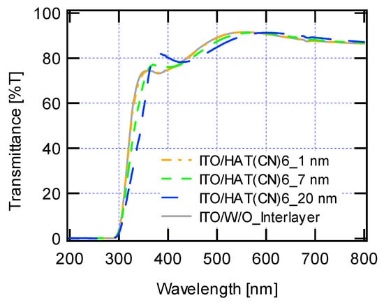
Figure 1.
(Color online) Transmittance–wavelength characteristics.
Figure 2 shows current density–voltage characteristics with log-linear scale with HAT(CN)6 thickness variation. The devices consisted of ITO/Interlayer X [X = HAT(CN)6 (1, 7, 20 nm)], or without Interlayer/α-NPD (95 nm)/Alq3:C545T (25 nm, 1%)/BPhen (25 nm)/LiF (1 nm)/Al (150 nm). The current density of the devices with ITO/Interlayer X [X = HAT(CN)6 (1, 7, 20 nm)], or without Interlayer were evaluated as 0.60720, 0.77299, 0.07841 and 0.00008 mA/cm2, respectively, at 2.6 V. The current density of the devices with ITO/Interlayer X [X = HAT(CN)6 (1, 7, 20 nm)], or without Interlayer were evaluated as 23.37750, 45.04625, 18.92525 and 0.00301 mA/cm2, respectively, at 4.8 V. At a driving voltage of 2.6 V, the device with 7 nm HAT(CN)6 achieved a current density 9.86-times higher than that with 20 nm HAT(CN)6. The current density of the device with 7 nm HAT(CN)6 was 9574-times higher than that without an interlayer. At a driving voltage of 4.8 V, the device with 7 nm HAT(CN)6 achieved a current density 2.38-times higher than that with 20 nm HAT(CN)6. The current density of the device with 7 nm HAT(CN)6 was 14,954-times higher than that without an interlayer. The current increase (2.38 times) of the device with 7 nm HAT(CN)6 relative to that with 20 nm HAT(CN)6 at a high driving voltage of 4.8 V was significantly lower than the current increase (9.86 times) of the device with 7 nm HAT(CN)6 at a low driving voltage of 2.6 V.
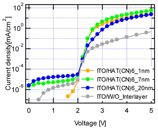
Figure 2.
(Color online) Current density–voltage characteristics with linear-log scale where the device structure is ITO/Interlayer X [X = HAT(CN)6 (1, 7, 20 nm)], or without Interlayer/α-NPD (95 nm)/Alq3:C545T (25 nm, 1%)/BPhen (25 nm)/LiF (1 nm)/Al (150 nm).
Figure 3 shows a low driving voltage range of the current density–voltage characteristics with linear–linear scale with HAT(CN)6 thickness variation. The current density of the devices with ITO/ Interlayer X [X = HAT(CN)6 (1, 7, 20 nm)], or without Interlayer were evaluated as 0.00137, 0.00145, 0.00089 and 0.00002 mA/cm2, respectively, at 2.2 V. The work functions of ITO/Interlayer X [X = HAT(CN)6 (1, 7, 20 nm)], or without Interlayer were estimated to be 5.1, 5.4, 5.65 and 4.7 eV, respectively [,]. The work function of α-NPD was estimated to be 5.4 eV []. As shown in Figure 2, 7 nm HAT(CN)6, used as the interlayer, and α-NPD showed very steep initial current density increases, as there was no injection barrier. The 1 nm HAT(CN)6 device exhibited slightly lower current density characteristics than the 7 nm HAT(CN)6 device, due to the presence of an injection barrier of 0.3 eV. Since the gap between the HOMO (Highest Occupied Molecular Orbital) level of α-NPD and the LUMO level of HAT(CN)6 is under 0.5 eV, the carrier transport between the two materials is easy. The carrier ladder effect and carrier transport mechanism resulting from the introduction of HAT(CN)6 led to excellent current density characteristics [,].
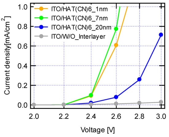
Figure 3.
(Color online) Enlarged low driving voltage range of current density–voltage characteristics with linear–linear scale where the device structure is ITO/Interlayer X [X= HAT(CN)6 (1, 7, 20 nm)], or without Interlayer/α-NPD (95 nm)/Alq3:C545T (25 nm, 1%)/BPhen (25 nm)/LiF (1 nm)/Al (150 nm).
The carrier transport between HAT(CN)6 and α-NPD is described in Figure 4 [,]. The Fermi level is contiguous to the conduction band for HAT(CN)6. The Fermi level is contiguous to the HOMO level for α-NPD. Specifically, the HOMO level for α-NPD is about 1.1 eV away from the conduction band of HAT(CN)6. In this regard, the carrier-transport process from the HOMO level for α-NPD to the conduction band of HAT(CN)6 is deemed easy. Simply put, the device with 20 nm HAT(CN)6, which has bulk characteristics, allows for easier carrier transport, and this is why the device exhibited an improvement in current density under the high driving voltage condition, compared to the devices equipped with 1 and 7 nm thin-film HAT(CN)6. In contrast, the device without an interlayer showed the worst current density characteristics, due to the hole injection barrier. HAT(CN)6 has a work function that varies with thickness and thus can be used as an excellent interlayer matching a hole transport layer.
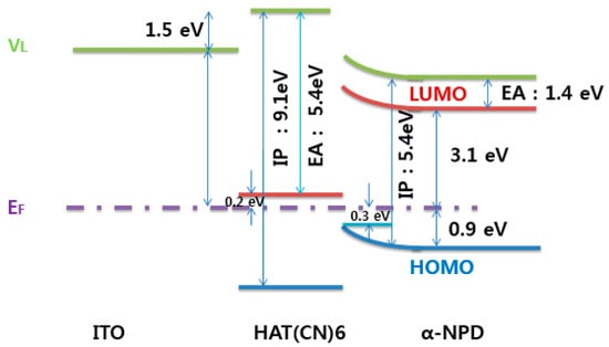
Figure 4.
(Color online) Energy level alignment at the ITO/ HAT(CN)6/α-NPD interface [,]: EF is the Fermi level, VL is a vacuum level, EA (electron affinity.) is electron affinity and Ip is ion potential [,].
Figure 5 shows luminance–voltage characteristics with log-linear scale with HAT(CN)6 thickness variation. As shown in Figure 5, the driving voltage starts from 2.8 V. This is because a luminance measurement system is divided into a current–voltage system and a current–voltage–luminance system, and is, therefore, forcibly converted to the current–voltage–luminance system from 2.8 V. The devices showed luminance–voltage characteristics similar to the current density–voltage characteristics. The device using 7 nm HAT(CN)6 showed the best luminance characteristics. On the other hand, the device without an interlayer showed the worst luminance characteristics.
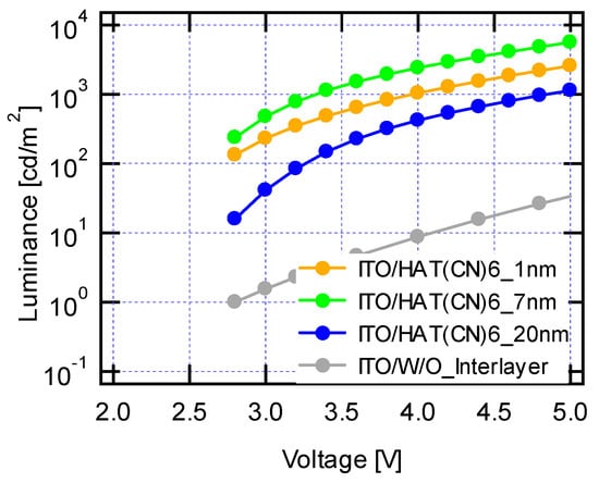
Figure 5.
(Color online) Luminance–voltage characteristics with log-linear scale where the device structure is ITO/Interlayer X [X = HAT(CN)6 (1, 7, 20 nm)], or without Interlayer/α-NPD (95 nm)/Alq3:C545T (25 nm, 1%)/BPhen (25 nm)/LiF (1 nm)/Al (150 nm).
Figure 6 shows luminance–current density characteristics with a log–log scale with HAT(CN)6 thickness variation. The devices using 1 and 7 nm thin-film HAT(CN)6 as the interlayer showed similar luminance characteristics. The sufficient hole injection by the devices using thin-film HAT(CN)6 affects the luminance efficiency. Thus, the devices exhibited similar luminance–current density characteristics.
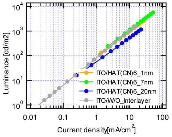
Figure 6.
(Color online) Luminance–current density characteristics with log–log scale where the device structure is ITO/Interlayer X [X = HAT(CN)6 (1, 7, 20 nm)], or without Interlayer/α-NPD (95 nm)/Alq3:C545T (25 nm, 1%)/BPhen (25 nm)/LiF (1 nm)/Al (150 nm).
Figure 7 shows current efficiency–voltage characteristics with linear–linear scale with HAT(CN)6 thickness variation. The device using 7 nm HAT(CN)6 exhibited a maximum current efficiency of 10.8 cd/A. The device using 1 nm HAT(CN)6 exhibited a maximum current efficiency of 9.4 cd/A. The device using 20 nm HAT(CN)6 exhibited a maximum current efficiency of 6.1 cd/A. The device without HAT(CN)6 showed an increasing current efficiency with an initial current efficiency of 5.9 cd/A. The devices with 7 nm HAT(CN)6 as the interlayer exhibited excellent current efficiency–voltage characteristics, without the collapse of the carrier balance, due to proper hole injection and carrier transport mechanism. The device with 20 nm HAT(CN)6 as the interlayer exhibited a low current efficiency, due to the collapse of the carrier balance resulting from the transport of many carriers, caused by bulk characteristics. The device without an interlayer showed a low current efficiency, due to the poor carrier balance resulting from the decreased probability of recombination of holes and electrons, caused by poor hole injection due to the hole injection barrier.
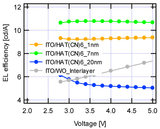
Figure 7.
(Color online) EL efficiency–voltage characteristics with linear–linear scale where the device structure is ITO/Interlayer X [X = HAT(CN)6 (1, 7, 20 nm)], or without Interlayer/α-NPD (95 nm)/Alq3:C545T (25 nm, 1%)/BPhen (25 nm)/LiF (1 nm)/Al (150 nm).
As a result, 7 nm thin-film HAT(CN6), which exhibited the best performance both in terms of driving voltage and current efficiency, was determined to have the optimal thickness for the device fabricated in the present study.
Figure 8 shows external quantum efficiency–current density characteristics with linear–linear scale with HAT(CN)6 thickness variation. Among the devices used, the device using 7 nm HAT(CN)6 as the interlayer achieved an external quantum efficiency of 2.96%. It achieved good external quantum efficiency, due to the proper carrier balance of holes and electrons.
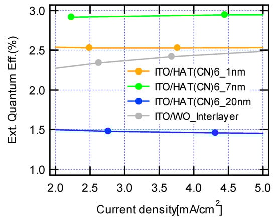
Figure 8.
(Color online) External quantum efficiency–current density characteristics with linear–linear scale where the device structure is ITO/Interlayer X [X = HAT(CN)6 (1, 7, 20 nm)], or without Interlayer/α-NPD (95 nm)/Alq3:C545T (25 nm, 1%)/BPhen (25 nm)/LiF (1 nm)/Al (150 nm).
It was possible to obtain an OLED with excellent driving voltage and current efficiency by optimizing the thickness of the thin film of HAT(CN)6 as an interlayer.
4. Conclusions
In this paper, we conducted an in-depth study of the electro-optical energy properties of devices using HAT(CN)6 as an interlayer. Transmittance in the wavelength range, including the visible light region, was investigated by varying the thickness of HAT(CN)6 on an ITO substrate. As a result, the devices were found to have a maximum transmittance of about 91.5% regardless of the thickness of HAT(CN)6 deposited on the ITO substrate. However, as the thickness of the HAT(CN)6 increased, the graph was shifted to a slightly longer wavelength. In the study of current density–voltage characteristics at a low voltage with HAT(CN)6 thickness variation, the devices with 1 and 7 nm thin-film HAT(CN)6 as the interlayer exhibited excellent current density characteristics, due to the carrier ladder effect and carrier transport phenomena by HAT(CN)6. On the other hand, the device with 20 nm HAT(CN)6 did not perform a proper hole injection function as an interlayer, due to its bulk characteristics. However, at a high driving voltage, it showed a rapidly increasing current density due to carrier transport phenomena. The device without an interlayer showed the worst current density–voltage characteristics due to poor hole injection.
In this study of current efficiency–voltage characteristics with HAT(CN)6 thickness variation, devices with thin-film HAT(CN)6 achieved good current efficiency. The devices using thin-film HAT(CN)6 as an interlayer showed good current efficiency, without the collapse of the carrier balance due to proper hole injection and carrier transport phenomena. The device without an interlayer exhibited lower current efficiency than the devices using thin-film HAT(CN)6 as an interlayer, due to poor hole injection caused by the hole injection barrier. This shows that the electro-optical properties of the devices using HAT(CN)6 as the interlayer are dominated by hole injection, which is controlled by varying the thickness of HAT(CN)6 as the interlayer, unlike constant electron injection from the cathode. HAT(CN)6 has a work function that varies with thickness. Thus, it is expected to serve as an excellent interlayer in OLEDs.
Author Contributions
For research articles with several authors, a short paragraph specifying their individual contributions must be provided. The following statements should be used “conceptualization, H.-G.P.; methodology, H.G.P; validation, S.G.P; formal analysis, S.G.P; investigation, H.-G.P.; resources, S.-G.P.; data curation, H.-G.P.; writing—original draft preparation, H.-G.P.; writing—review and editing, S.-G.P.; visualization, H.-G.P.; supervision, S.-G.P.; project administration, S.-G.P.; funding acquisition, H.-G.P.
Funding
This research was supported by Changwon National University in 2019~2020.
Acknowledgments
The authors would like to thank S.-H. Kim, M.-K. Ma and J.-S. Kim from SFC Company for their help in device fabrication and characterization.
Conflicts of Interest
The authors declare no conflict of interest.
References
- Pope, M.; Kallmann, H.P.; Magnante, P. Electroluminescence in Organic Crystals. J. Chem. Phys. 1963, 38, 2042–2043. [Google Scholar] [CrossRef]
- Tang, C.W.; VanSlyke, S.A. Organic electroluminescent diodes. Appl. Phys. Lett. 1987, 51, 913–915. [Google Scholar] [CrossRef]
- Tokito, S.; Taga, Y. Organic electroluminescent devices fabricated using a diamine doped MgF2 thin film as a hole-transporting layer. Appl. Phys. Lett. 1995, 66, 673–675. [Google Scholar] [CrossRef]
- Van Slyke, S.A.; Chen, C.H.; Tang, C.W. Organic electroluminescent devices with improved stability. Appl. Phys. Lett. 1996, 69, 2160–2162. [Google Scholar] [CrossRef]
- Hwang, S.G.; Park, H.G.; Park, M.H.; Park, S.G. Homeotropic alignment behavior of liquid crystal molecules on self-assembled monolayers with fluorinated alkyl chain. J. Vac. Sci. Technol. A 2018, 36, 041401-1–041401-4. [Google Scholar] [CrossRef]
- Aziz, H.; Popovic, Z.D.; Hu, N.X.; Hor, A.M.; Xu, G. Degradation Mechanism of Small Molecule-Based Organic Light-Emitting Devices. Science 1999, 283, 1900–1902. [Google Scholar] [CrossRef] [PubMed]
- Tao, Y.; Wub, K.; Huang, K.; Perng, T. Odd–even modulation of electrode work function with self-assembled layer: Interplay of energy barrier and tunneling distance on charge injection in organic light-emitting diodes. Org. Electron. 2011, 12, 602–608. [Google Scholar] [CrossRef]
- Kang, H.; Kim, J.H.; Kim, J.K.; Seo, J.; Park, Y. Interface Electronic Structure of a Strongly Electron Withdrawing Molecule on an Indium-tin-oxide Surface. J. Korean Phys. Soc. 2011, 59, 3060–3063. [Google Scholar] [CrossRef]
- Huang, P.R.; He, Y.; Cao, C.; Lu, Z.H. The origin of the high work function of chlorinated indium tin oxide. NPG Asia Mater. 2013, 5, 1–6. [Google Scholar] [CrossRef]
- Sharma, A.; Haldi, A.; Hotchkiss, P.J.; Marder, S.R.; Kippelen, B. Effect of phosphonic acid surface modifiers on the work function of indium tin oxide and on the charge injection barrier into organic single-layer diodes. J. Appl. Phys. 2009, 105, 074511-1–074511-6. [Google Scholar] [CrossRef]
- Yang, J.P.; Bussolotti, F.; Li, Y.Q.; Zeng, X.H.; Kera, S.; Tang, J.X.; Ueno, N. The role of gap states on energy level alignment at an α-NPD/HAT(CN)6 charge generation interface. Org. Electron. 2015, 24, 120–124. [Google Scholar] [CrossRef]
- Kim, Y.K.; Kim, J.W.; Park, Y. Energy level alignment at a charge generation interface between 4,4′ -bis(N-phenyl-1-naphthylamino)biphenyl and 1,4,5,8,9,11-hexaazatriphenylene-hexacarbonitrile. Appl. Phys. Lett. 2009, 94, 063305-1–063305-3. [Google Scholar] [CrossRef]
© 2019 by the authors. Licensee MDPI, Basel, Switzerland. This article is an open access article distributed under the terms and conditions of the Creative Commons Attribution (CC BY) license (http://creativecommons.org/licenses/by/4.0/).