Article

Impact of K+ Doping on Modulating Majority Charge Carrier Type and Quality of Perovskite Thin Films by Two-step Solution Method for Solar Cells

1
Beijing Advanced Innovation Center for Materials Genome Engineering, Research Center for Sensor Technology, Beijing Key Laboratory for Sensor, MOE Key Laboratory for Modern Measurement and Control Technology, School of Applied Sciences, Beijing Information Science and Technology University, Jianxiangqiao Campus, Beijing 100101, China
2
State Key Laboratory on Integrated Optoelectronics, Institute of Semiconductors, Center of Materials Science and Optoelectronics Engineering, University of Chinese Academy of Sciences, Chinese Academy of Sciences, Beijing 100864, China
*
Author to whom correspondence should be addressed.
Coatings 2019, 9(10), 647; https://doi.org/10.3390/coatings9100647
Submission received: 15 August 2019 / Revised: 27 September 2019 / Accepted: 27 September 2019 / Published: 6 October 2019

Abstract

:
Traditional hetero-junction perovskite solar cells are composed of light-absorbing layers, charge carrier-transporting layers, and electrodes. Recently, a few papers on homo-junction perovskite solar cells have been studied. Here, we studied the effect of K+ doping on TiO2/PbI2 interface quality, perovskite film morphology, photo-physical properties, and majority carrier type. In particular, the K+ extrinsic doping can modulate the majority carrier type of the perovskite thin film. The study indicated that the interface between the perovskite layer and the TiO2 layer deteriorates with the increase of K+ doping concentration, affecting the electron transport ability from the perovskite film to the TiO2 layer and the photo-physical properties of the perovskite layer by K+ doping. In addition, the majority charge carrier type of perovskite thin films can be changed from n-type to p-type after K+ extrinsic doping, and the corresponding hole concentration increased to 1012 cm−3. This approach of modulating the majority charge carrier type of perovskite thin film will pave the way for the investigation of perovskite homo-junction by extrinsic doping for solar cells.

1. Introduction

In the past decade, the development of perovskite solar cells has drawn intensive attention due to its potential in the next generation low-cost solution process of photovoltaic materials. During the research of perovskite solar cells, devices applying these perovskite materials have achieved great progress in both mesoporous structure and planar hetero-junction structure. However, perovskite solar cells still have some problems, such as majority charge carrier types, electronic conductivity of perovskite, and the impact of doping on device performance and photo-physical properties [1,2,3].
In order to investigate the effect of self-doping on device performance, Huang Jinsong et al. revealed that CH3NH3PbI3 can be either n-type or p-type self-doped by changing the ratio of two precursors for perovskite formation [4]. On the basis of this, Li Meicheng’s research group fabricated a perovskite p-n homo-junction structure, via a combined deposition processing method. In addition, this experiment that the corresponding holes concentrations can be as low as 1010 cm–3, which is insufficient to form an effective p–n junction [5]. Theoretical research predicted that the majority charge carrier type of perovskite thin film can be modulated from n-type to p-type by K+ extrinsic doping.In the study of the extrinsic doping of perovskite, Shan Jia et al. found that film quality can be improved by K+ doping [6]. Tao Ling et al. showed that different concentrations of K+ doping affect the morphology of perovskite film quality [7]. Zeguo Tang et al. results revealed that incorporating a small amount of K+ into the double organic cation perovskite absorber improved the photovoltaic performance of PSCs significantly, and K+ incorporation diminished I-V hysteresis [8]. In addition, in March 2018, Mojtaba Abdi-Jalebi, Zahra Andaji-Garmaroudi and colleagues demonstrated the inhibition of transient photoinduced ion-migration processes across a wide range of mixed halide perovskite bandgaps in materials that exhibit bandgap instabilities when unpassivated [9]. In December of the same year, Mojtaba Abdi-Jalebi, Zahra Andaji-Garmaroudi and colleagues directly compared the optoelectronic properties and stability of thin films when passivating triple-cation perovskite films with potassium or rubidium species. This research indicates that tolerance to higher loadings of potassium can achieve superior luminescent properties with potassium passivation [10]. Dae-Yong Son, Seul-Gi Kim and colleagues discovered that potassium ion plays an important role in controlling the defects [11]. However, a few studies predicted that the majority charge carrier type can be modulated, but perovskite homo-junction by extrinsic doping of solar cells was not found.
In this manuscript, this study indicated that the majority charge carrier type of perovskite thin film can be modulated from n-type to p-type by K+ extrinsic doping; the corresponding hole concentration was increased to 1012 cm−3, which is relatively sufficient to form an effective p–n junction. Meanwhile, the K+ doping affects TiO2/PbI2 interface quality, perovskite film morphology, and photo-physical properties. Our study will pave the way for the investigation of perovskite homo-junction by extrinsic doping for solar cells.

2. Materials and Methods

2.1. Materials

Fluorine-doped SnO2 (FTO) substrates were obtained from Dalian Hepta Chroma Solar Technology Development Corp (Dalian, China). N, N-dimethylformamide (DMF) and dimethyl sulfoxide (DMSO) were purchased from Sa’en Chemical Technology Corp (Shanghai, China). Lead(II) iodide(PbI2, Cas No. 10101-63-0, yellow crystalline powder in appearance, purity >99.99%), 18NR-T TiO2 paste (mp-TiO2), acidic titanium dioxide solution (bl-TiO2), methyl ammonium iodide (CH3NH3I, MAI, Cas No.14965-49-2, white powder in appearance, purity 99.5%), Isopropyl alcohol (IPA), Commercial 2,2′,7,7′tetrakis-(N,N-dip-methoxyphenylamine)9,9′spirobifluorene solution (Spiro-OMeTAD, Cas No. 207739-72-8, yellow powder in appearance, purity 99.5%), and KI were purchased from Xi’an Polymer Light Technology Corp (Xi’an, China) [12,13].

2.2. Device Fabrication

The FTO surface was washed with glass water (deionized water: acetone: isopropanol = 1:1:1, volume ratio) and sonicated for 20 min. After sonication, FTO was rinsed thoroughly with deionized water and then dried in a dry box for 70 min. For the preparation of the TiO2 dense layer, we spin-coated the TiOx acidic solution at 2000 rpm for 60 s and then annealed it at 100 °C for 10 min. Finally, it was sintered at 500 °C for 30 min in a muffle furnace. The mesoporous-TiO2 layer was made by spin-coating the 18NR-T TiO2 at 2000 rpm for 60 s and then it was annealed at 100 °C for 10 min. Finally, it was sintered at 500 °C for 30 min in a muffle furnace.
For the preparation of the perovskite layer, 0.5993 g of PbI2 was dissolved in a mixed solution of N, N-dimethylformamide (DMF) and dimethyl sulfoxide (DMSO) (volume ratio of DMF to DMSO was 0.95:0.05). Then, 0.00664, 0.01328 and 0.01992 g of KI powder were mixed with the 1 mL pure PbI2 solution to obtain a precursor solution having a concentration of 0.04, 0.08 and 0.12 mol/L, respectively. To obtain a MAI solution, 0.072g of MAI was dissolved in 1 mL isopropyl alcohol solution. The prepared PbI2 and precursor solution with different doping concentrations were spin-coated on the mesoporous-TiO2 layer at 1500 rpm for 30 s, and the MAI solution was spin-coated on the PbI2 layer at 1500 rpm for 30 s. A perovskite layer was formed after annealing on a hot plate at 150°C for 15 min.
For the preparation of the hole transport layer, Spiro-MeOTAD, 260 mg of Li-TFST was dissolved in 5 mL of Acetonitrile solution, 14.46 mg of Spiro-MeOTAD powder was dissolved in 2 mL of Chlorobenzene, and 35 μL tBP was added. Finally, the two solutions prepared were mixed. We spin-coated the Spiro-MeOTAD solution at 3000 rpm for 30 s. Finally, the FTO substrates were used to collect the soot of a burning candle as counter electrode (CE) and these spongy carbon films on FTO glasses were then pressed on the as-prepared uncompleted devices. The spongy carbon films on the counter electrode have a certain uniformity. The average thickness of spongy carbon films is about 300 nm. The preparation of the entire device is done in air.

2.3. Characterization

An X-ray diffractometer (XRD) (Broker, D8 Focus, Beijing, China) was used to obtain XRD spectra from samples of perovskite films deposited on mp-TiO2/bl-TiO2/FTO substrates. The morphologies of these perovskite films were watched by a scanning electron microscope (SEM) (Zeiss SIGMA, Oberkochen, Germany). The as-prepared devices were measured under full sun illumination (AM 1.5, 100 mW/cm2); the active area of the solar cells was 0.2cm2. However, the absorption spectra of perovskite films with different doping concentrations of K+ were analyzed by an ultraviolet visible (UV-vis) absorption spectrometer (Avantes, Apeldoom, The Netherlands), and the photoluminescence (PL) spectrum was examined by a LabRAW HR800 PL testing system (HORIBA JObin Yvon, Paris, France). The carrier concentration and mobility were measured by Hall Impact Measurement System (HL5500-1217-0180, Milpitas, CA, USA).

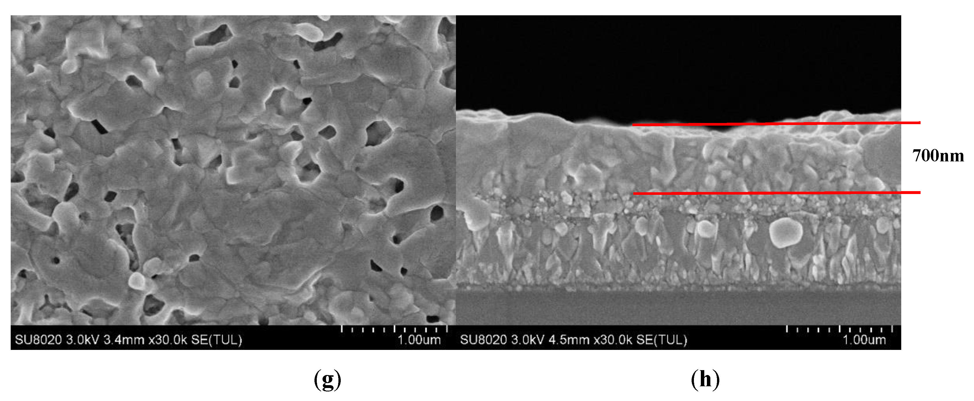
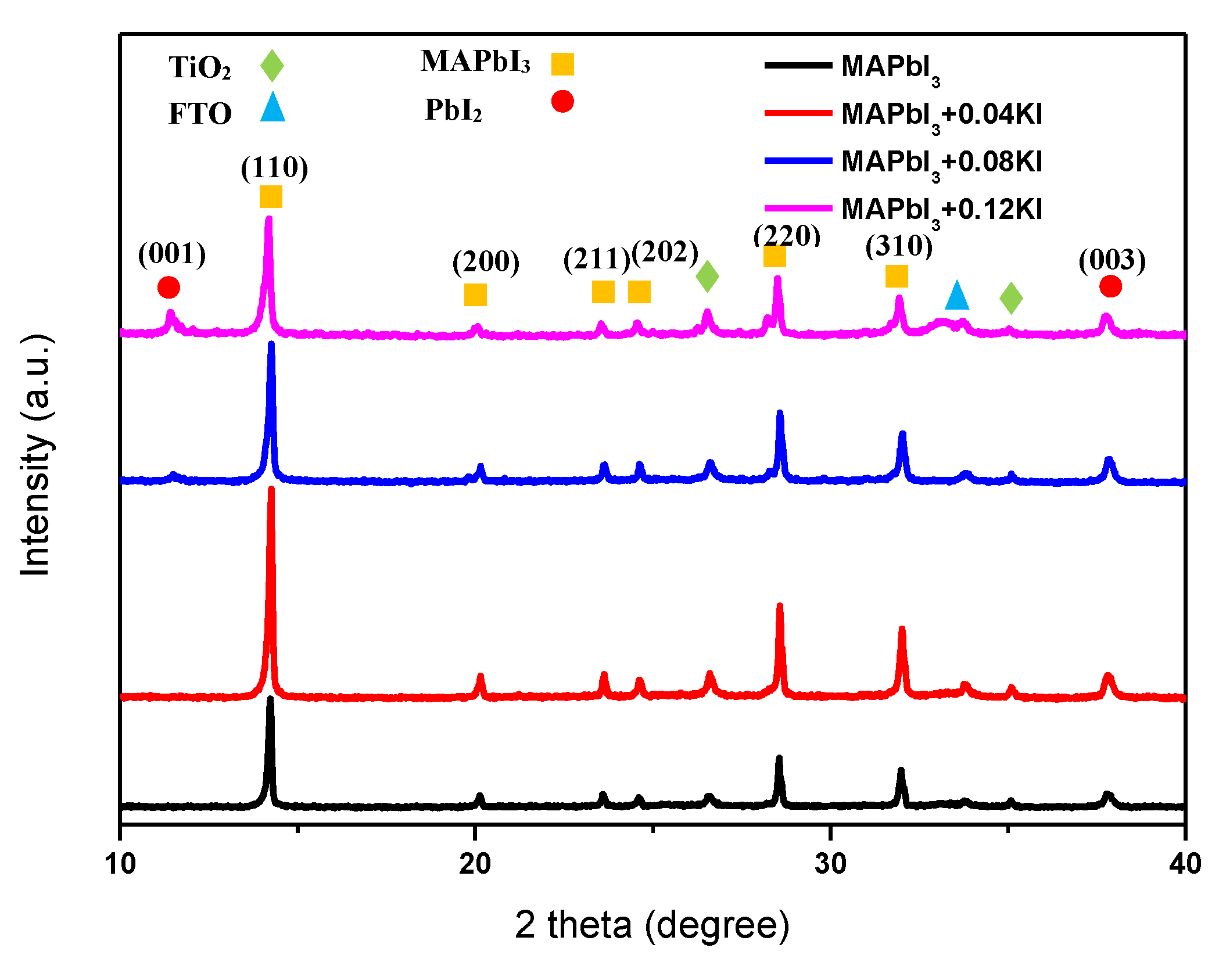
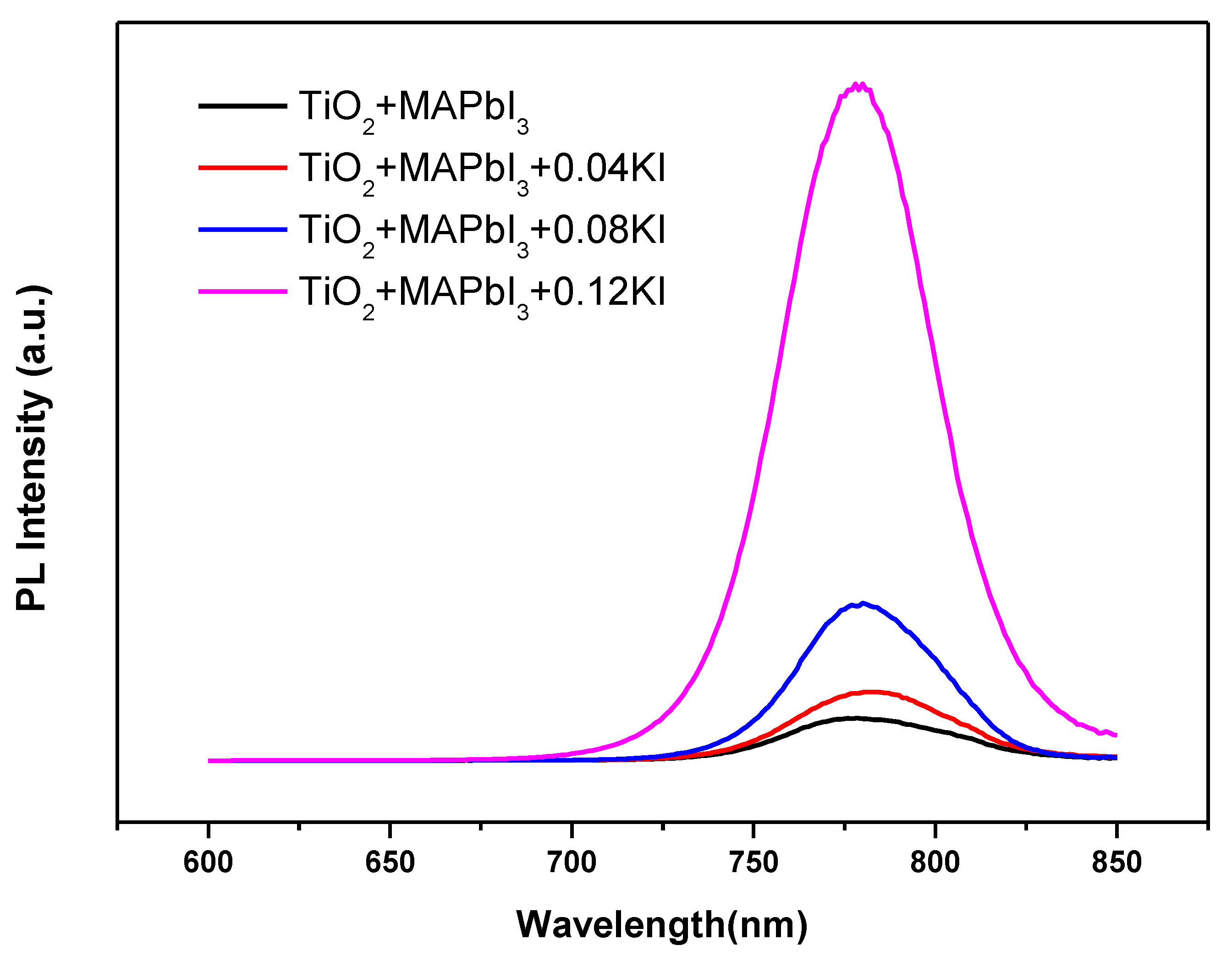
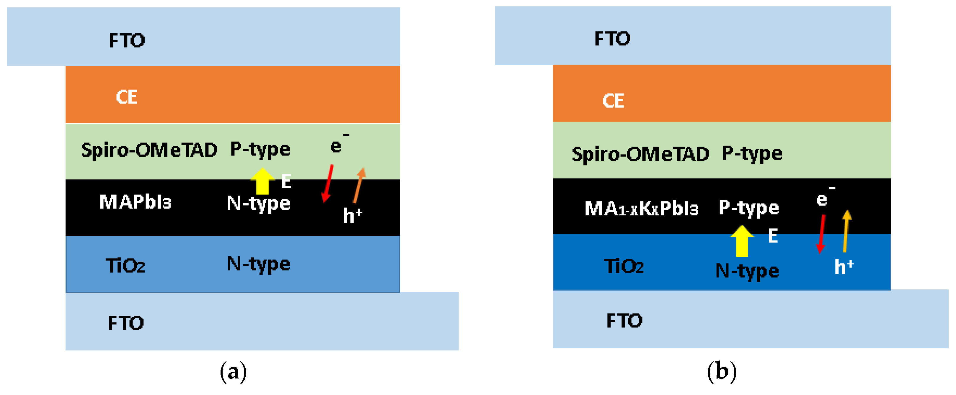
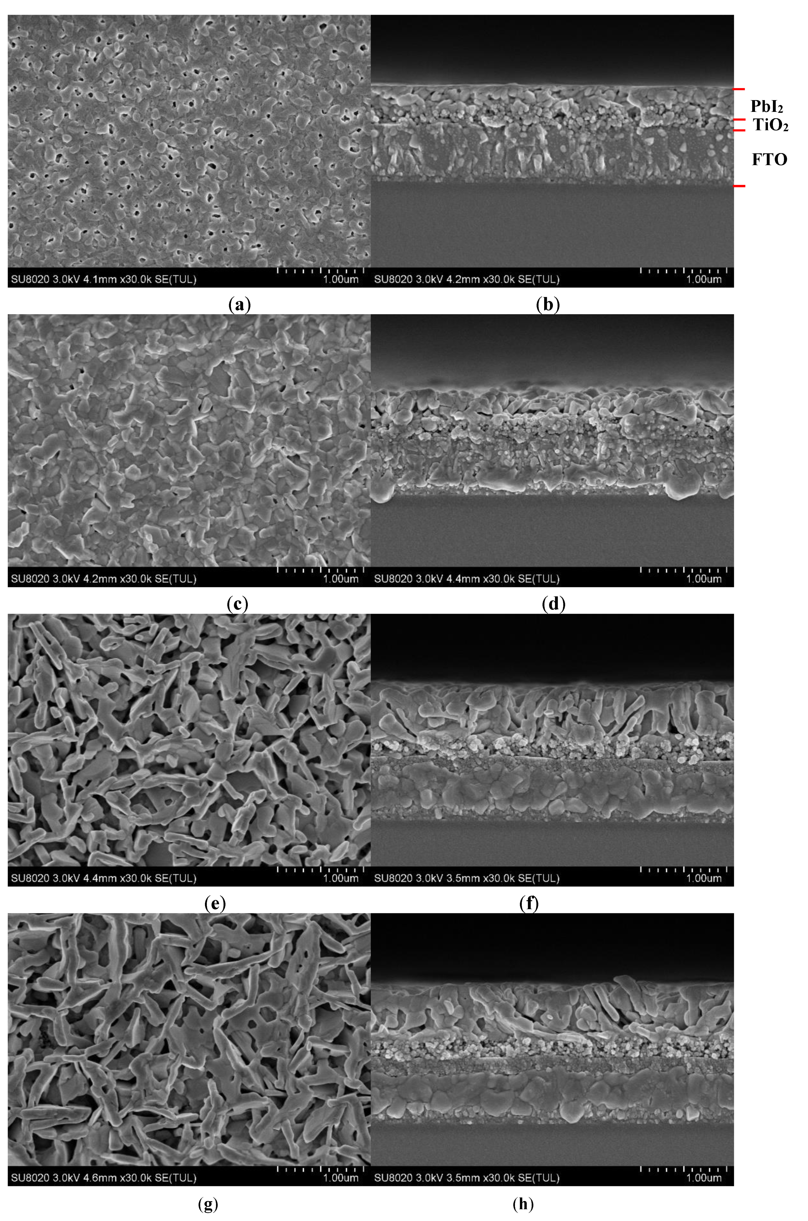
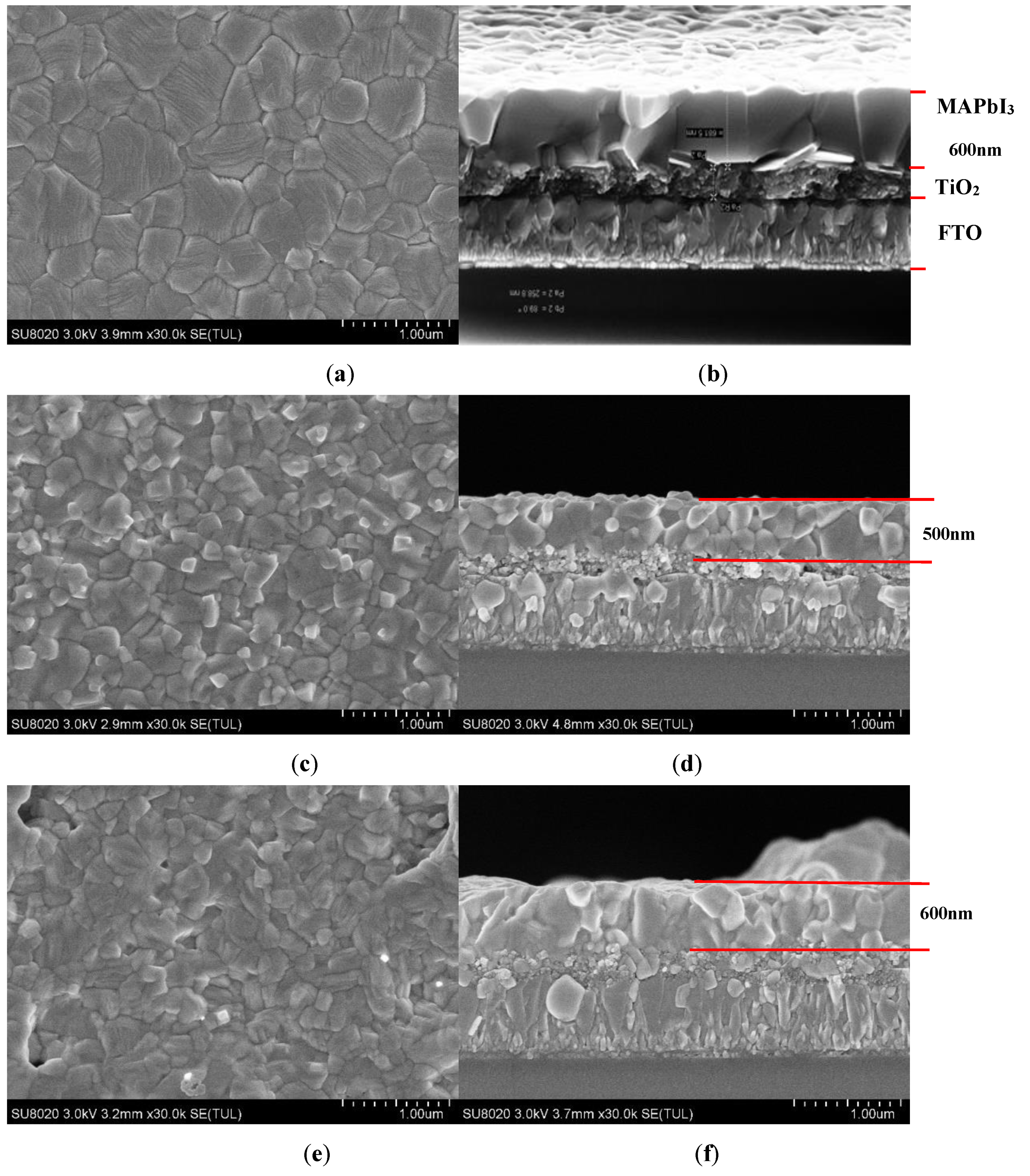
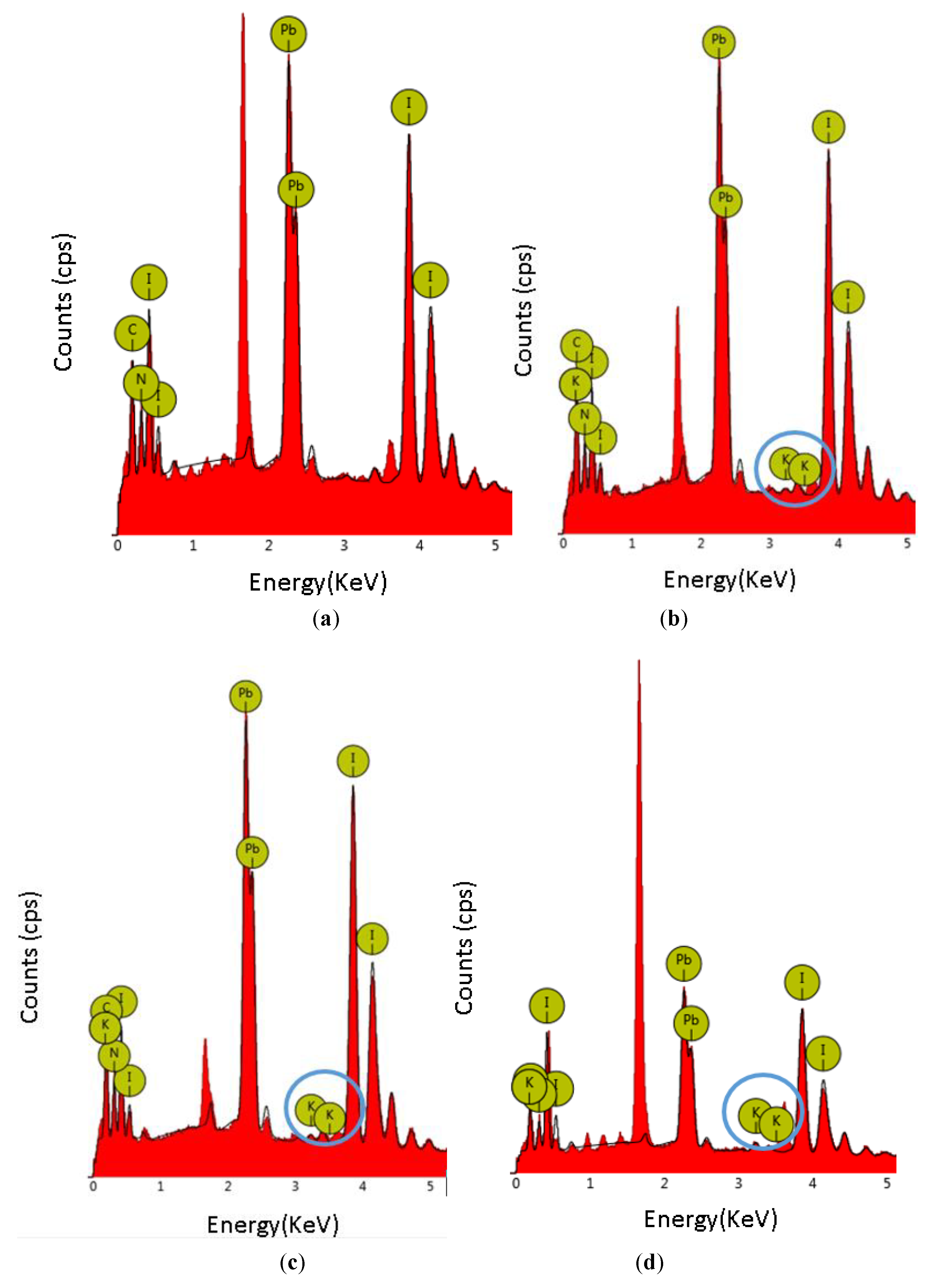
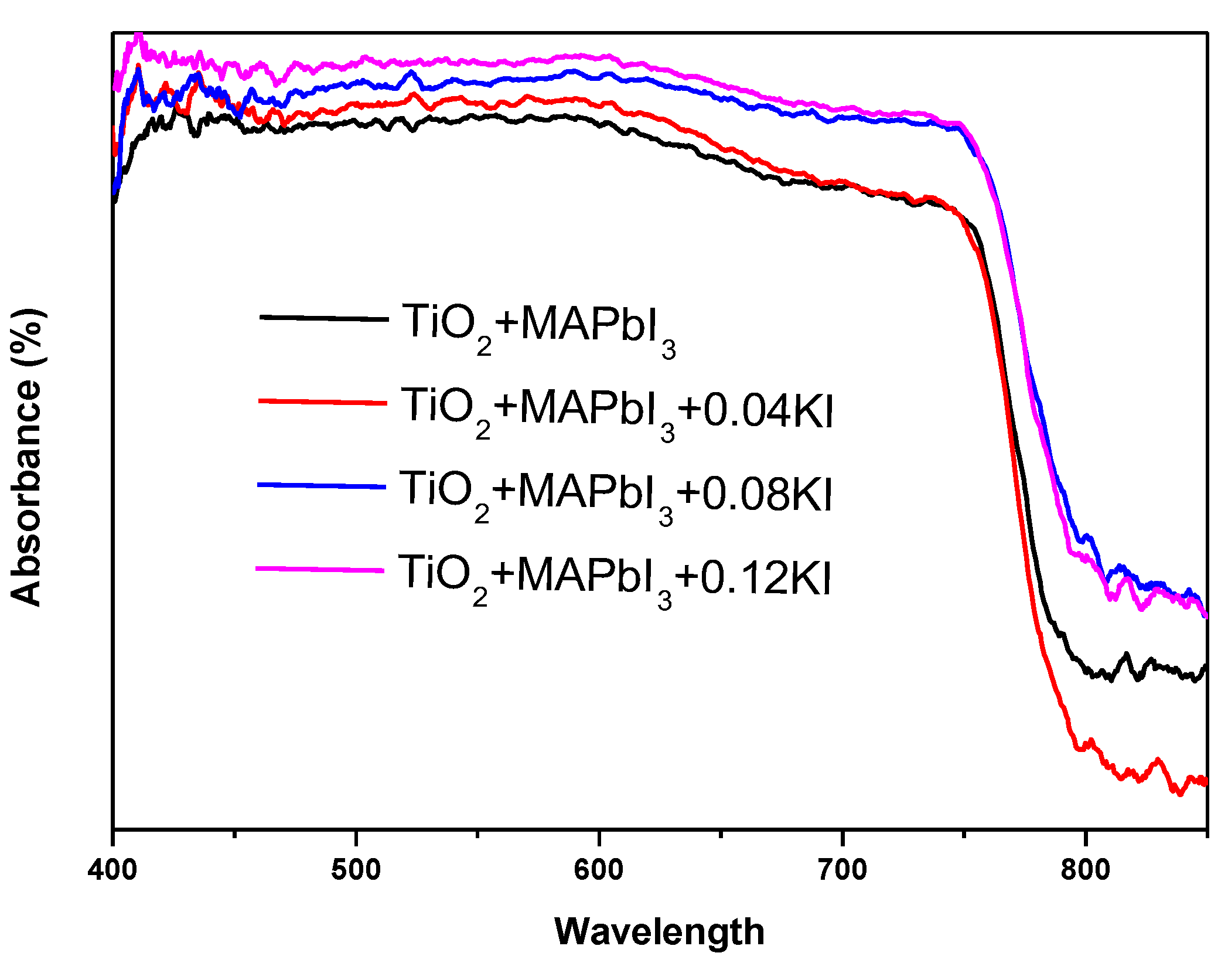
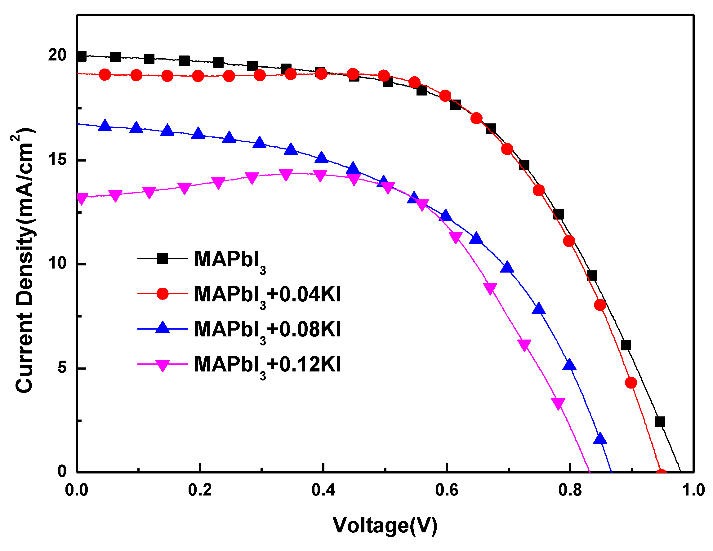
3. Results and Discussion

The Scanning Electron Microscope (SEM) image of the surface and cross-section of PbI2 film are shown in Figure 1. From Figure 1a, it can be seen that the un-doped PbI2 film is not dense, and the grain size of PbI2 is about 150 nm. The film has a large number of pin-holes, and the diameter of the pin-hole is about 100 nm. These pin-holes in the PbI2 layer contribute to the full reaction of the MAI solution with PbI2 and promote the formation of a perovskite thin film. From Figure 1b, few defects are observed between PbI2 and the mesoporous-TiO2 layer, which will facilitate electron transport. Figure 1c shows the surface of the PbI2+0.04KI film; it can be seen that the PbI2 crystal grains have become larger, the size is about 300 nm. However, the grain boundaries become darker. Compared with the un-doped PbI2 film, the size of the pin-hole becomes smaller, which is not conducive to the reaction of PbI2 with MAI to form a perovskite film. Figure 1d is a corresponding cross-section, it shows that the pin-holes between the PbI2 layer and the mesoporous-TiO2 layer become larger. There are defects between the TiO2/PbI2 interfaces, which reduces the transmission capability of electrons between the TiO2/PbI2 interfaces. Figure 1e is the surface of PbI2+0.08KI film; compared with low concentrations (≤ 0.04 mol/L), a large number of pin-hores were observed on the surface of the PbI2 film. Figure 1f is a corresponding cross-section, it can be seen that the surface of the PbI2 film is uneven and the defects between the TiO2/PbI2 interfaces increased. The transmission capability of electrons is reduced. Figure 1g is the surface of the PbI2+0.12KI film. The surface is rougher than 0.08M. Figure 1h is the cross-section, it displays that the defects increased on the TiO2/PbI2 interface. The PbI2 surface becomes rough. From SEM of PbI2, as the K+ doping concentration increases, the interfacial contact of TiO2/PbI2 deteriorates, which may affect the electron transport capability between the perovskite layer and the TiO2 layer [14,15,16].
Figure 2 is an SEM of the surface and cross section of different concentrations of K+ doped perovskite films. From Figure 2a, it can be seen that the surface of un-doped perovskite film is smooth, has large perovskite grain, and is pin-hole-free. Figure 2b is the corresponding cross-section. It can be seen that the crystal grain size is large. Figure 2c shows the surface of the MAPbI3+0.04KI film, it can be seen that the surface becomes rough and the grain size becomes small. Figure 2d displays that the surface of the film is rough. Figure 2e shows the surface of the MAPbI3 + 0.08 KI film, it displays that the grain size becomes small, and the grain boundaries of the perovskite film become darker. Figure 2f is a corresponding cross-section; the cross-section exhibits that the surface of the perovskite film is uneven, and the grain boundary becomes darker. From Figure 2g, the film is not compact anymore, there is incomplete surface coverage, and the grain boundaries are darker. Figure 2h is the cross section, it can be seen that the surface of the perovskite layer becomes rougher. From the SEM image of the perovskite film, as the K+ doping concentration increases, the number of pin-holes in the perovskite layer increases and the grain size decreases. The surface of the perovskite becomes rough [13,15,16]. The thickness of the perovskite layer with doping concentrations of 0, 0.04, 0.08 and 0.12 mol/L are 600, 500, 600 and 700 nm, respectively. With the K+ doping concentration increase, the quality of the PbI2 layer deteriorates, and the quality of the perovskite film deteriorates.
Figure 3 shows the X-ray diffractometer (XRD) pattern of a perovskite film which has different K+ doping concentrations. From the XRD, the perovskite crystals of different K+ concentrations show that the doping with different K+ concentrations did not change the crystal structure of the perovskite [8]. From Figure 3, it can be seen that at low concentrations (≤ 0.04 mol/L), PbI2 does not precipitate. When the K+ doping concentration increases, precipitation of PbI2 is observed from the peak position of 12.56° (001). When the K+ doping concentration is 0.12 M, the XRD data of PbI2 shows a higher diffraction intensity than 0.08 M. The increase in the peak intensity of PbI2 is observed with the increase the of K+ doping concentration, resulting in an uneven surface on the perovskite film. This is consistent with the SEM rule of the perovskite layer [17,18,19].
Figure 4 is an Energy Dispersive Spectroscopy (EDS) diagram of a K+ doped perovskite film. It shows that the peak value of K+ in the perovskite film increases as the doping concentration increases, indicating that the perovskite film contains K+. Table 1 shows the atomic percentage of the K doped perovskite film EDS. It can be seen that as the doping concentration increases, the percentage of K atoms increases [8].
Table 2 is the Hall test parameters of the K+ doped perovskite on glasses. It can be seen from the table that the un-doped perovskite is an n-type semiconductor. After K+ doping, the majority carrier concentration of the perovskite has increased and it is a p-type semiconductor. This indicates that the two-step K+ doping causes the majority carrier type of the perovskite to change from n-type to p-type. Hall experiments have shown that the majority carrier type of perovskite can be regulated by K+ extrinsic doping. In addition, as shown in Hall effects test experiments, the holes concentration of p-type perovskite was tuned up to 1012 cm−3 by K+ extrinsic doping.
Figure 5 is an ultraviolet-visible (UV-vis) absorption spectrum of a perovskite layer having different K+ concentrations. It can be observed from Figure 5 that the wavelength has a relatively strong absorption peak at 440 to 750 nm. When un-doped, the light absorption intensity is the weakest. This is consistent with the SEM rule of the perovskite layer. With the K+ doping concentration increase, the surface of the perovskite films becomes rough, producing lower reflected light and enhancing light absorption [13,20].
Figure 6 is a photoluminescence (PL) spectrum of a perovskite layer of different K+ concentrations. We found that the emission peaks of the four perovskite films ranged from 720 nm to 820 nm. When un-doped, consistent with the SEM, the interface between the perovskite layer and the TiO2 layer is better, and the peak of PL is low, indicating that the number of photo-generated carriers injected into the TiO2 from the perovskite light-absorbing layer is the largest. With the K+ doping concentration increases, the interface quality of the perovskite layer and the TiO2 layer deteriorates, the PL intensity of the perovskite gradually increases, and the number of photo-generated carrier injected to the TiO2 layer from the perovskite light-absorbing layer decrease.
Consistent with the SEM image, the mass of the perovskite film and the interface quality of the perovskite layer and the TiO2 layer deteriorate with the increase of the K+ doping concentration. The photo-generated carrier number decreases from the perovskite layer being injected the TiO2 layer and the quenching ability of the carrier decreases [13,21,22].
Figure 7 is a reverse scan (RS) of density–voltage (J–V) curves of perovskite devices with different K+ concentrations. Table 3 shows the photovoltaic parameters of perovskite devices with different K+ concentrations. It can be seen from Figure 7 that the un-doped device and the different K+ concentrations of the doped devices can work normally, and the device performance deteriorates. In Table 3, with the K+ doping concentration increase, the short-circuit current density (Jsc), open-circuit voltage (Voc) and photoelectric conversion efficiency (PCE) of the perovskite device decrease. The research indicates that with the defect increase of the TiO2/PbI2 interface and the K+ doping concentration increase, the quality of the perovskite film deteriorates, and the number of photo-generated carriers injected into the TiO2 layer from the perovskite layer is reduced, and subsequently, the device performance deteriorates.
The structure of the device is shown in Figure 8. In order to display that the majority carrier type of the perovskite thin film can be modulated from n-type to p-type perovskite thin film by K+ extrinsic doping, we have prepared the un-doped n-type MAPbI3 and doped p-type MA1-XKXPbI3 devices. In Figure 8a, when the majority carrier type of the perovskite layer is n-type, the perovskite layer forms a p-n junction with the hole transport layer (Spiro-MeOTAD layer). Figure 8b, when the majority carrier type of the perovskite layer is p-type, the perovskite layer forms a p–n junction with the electron transport layer (TiO2 layer). The spongy carbon/FTO is employed as CE in perovskite photovoltaic devices. The preparation of the entire installation is done in the air.

4. Conclusions

In our research, it was found that the majority charge carrier type of perovskite thin film can be modulated from n-type to p-type by K+ extrinsic doping, and the corresponding hole concentration was increased to 1012 cm−3. The increase of K+ doping concentration results in the perovskite film having a rough surface, producing lower reflected light and enhancing light absorption. In addition, the quality of perovskite film and the interface quality of the perovskite layer and the TiO2 layer deteriorated with the increase of the K+ doping concentration, and the number of photo-generated carrier injected to the TiO2 layer from the perovskite light-absorbing layer decrease. Meanwhile, the Jsc and Voc of the perovskite device decreased with the K+ doping concentration increase. Our research will open the avenue for the investigation of perovskite homo-junction by combined p-type extrinsic doping and n-type self-doping for solar cells.

Author Contributions

Data curation, J.C.; Investigation, T.L. and C.C.; Methodology, D.C.; Supervision, X.Z.; Writing – original draft, Y.Y.

Funding

This research was funded by the project of the Natural Science Foundation of China (No. 61875186), the project of the Natural Science Foundation of Beijing (No. Z160002), the Key Research Projects of BISTU (2018-22, 2019-22, 2019-23, and 2019-27), and the Beijing Key Laboratory for Sensors of BISTU (No. 2019CGKF007).

Conflicts of Interest

The authors declare that they have no conflict of interest.

References

  1. Zhou, H.; Chen, Q.; Li, G.; Luo, S.; Song, T.B.; Duan, H.S.; Yang, Y. Interface engineering of highly efficient perovskite solar cells. Science 2014, 345, 542–546. [Google Scholar] [CrossRef] [PubMed]
  2. Yang, W.S.; Noh, J.H.; Jeon, N.J.; Kim, Y.C.; Ryu, S.; Seo, J.; Seok, S.I. High-performance photovoltaic perovskite layers fabricated through intramolecular exchange. Science 2015, 348, 1234–1237. [Google Scholar] [CrossRef] [PubMed]
  3. Eperon, G.E.; Burlakov, V.M.; Docampo, P.; Goriely, A.; Snaith, H.J. Morphological Control for High Performance, Solution-Processed Planar Heterojunction Perovskite Solar Cells. Adv. Funct. Mater. 2014, 24, 151–157. [Google Scholar] [CrossRef]
  4. Wang, Q.; Shao, Y.; Xie, H.; Lyu, L.; Liu, X.; Gao, Y.; Huang, J. Qualifying composition dependent p and n self-doping in CH3NH3PbI3. Appl. Phys. Lett. 2014, 105, 163508. [Google Scholar] [CrossRef]
  5. Cui, P.; Wei, D.; Ji, J.; Huang, H.; Jia, E.D.; Dou, S.Y. Planar p–n homojunction perovskite solar cells with efficiency exceeding 21.3%. Nat. Energy 2019, 4, 150–159. [Google Scholar] [CrossRef]
  6. Jiang, Q.; Zhang, L.; Wang, H.; Yang, X.; Meng, J.; Liu, H.; You, J. Enhanced electron extraction using SnO2 for high efficiency planar-structure HC (NH2)2PbI3-based perovskite solar cells. Nat. Energy 2017, 2, 16177. [Google Scholar] [CrossRef]
  7. Jia, S.; Wang, J.; Zhu, L. Enhancing the photovoltaic performance of perovskite solar cells by potassium ions doping. J. Mater. Sci. Mater. Electron. 2019, 30, 2057–2066. [Google Scholar] [CrossRef]
  8. Ling, T.; Zou, X.; Cheng, J.; Yang, Y.; Ren, H.; Chen, D. Modulating Surface Morphology Related to Crystallization Speed of Perovskite Grain and Semiconductor Properties of Optical Absorber Layer under Controlled Doping of Potassium Ions for Solar Cells. Materials 2018, 11, 1605. [Google Scholar] [CrossRef]
  9. Abdi-Jalebi, M.; Andaji-Garmaroudi, Z.; Cacovich, S.; Stavrakas, C.; Philippe, B.; Richter, J.M.; Lilliu, S. Maximizing and stabilizing luminescence from halide perovskites with potassium passivation. Nature 2018, 555, 497–501. [Google Scholar] [CrossRef]
  10. Abdi-Jalebi, M.; Andaji-Garmaroudi, Z.; Pearson, A.J.; Divitini, G.; Cacovich, S.; Philippe, B.; Stranks, S.D. Potassium- and Rubidium-Passivated Alloyed Perovskite Films: Optoelectronic Properties and Moisture Stability. ACS Energy Lett. 2018, 3, 2671–2678. [Google Scholar] [CrossRef]
  11. Son, D.Y.; Kim, S.G.; Seo, J.Y.; Lee, S.H.; Shin, H.; Lee, D.; Park, N.G. Universal Approach toward Hysteresis-Free Perovskite Solar Cell via Defect Engineering. J. Am. Chem. Soc. 2018, 140, 1358–1364. [Google Scholar] [CrossRef] [PubMed]
  12. Ren, H.Y.; Zou, X.P.; Cheng, J.; Ling, T.; Bai, X.; Chen, D. Facile solution spin-coating SnO2 thin film covering cracks of TiO2 hole blocking layer for perovskite solar cells. Coatings 2018, 8, 314. [Google Scholar] [CrossRef]
  13. Yao, Y.; Zou, X.; Cheng, J.; Chen, D.; Chang, C.; Ling, T.; Ren, H. Impact of Delay Time before Annealing MAI-PbI2-DMSO Intermediate Phase on Perovskite Film Quality and Photo-Physical Properties. Crystals 2019, 9, 151. [Google Scholar] [CrossRef]
  14. Yang, Y.; Zou, X.; Pei, Y.; Bai, X.; Jin, W.; Chen, D. Impact of doping of NaI monovalent cation halide on the structural, morphological, optical and optoelectronic properties of MAPbI3 perovskite. J. Mater. Sci. Mater. Electron. 2018, 29, 205–210. [Google Scholar] [CrossRef]
  15. Cheng, J.; Qiang, Y.; Zhou, C.; Shi, H.; Liu, H.; Geng, C.; Xie, Y. Impactive improvement of the photovoltaic performance of carbon-based perovskites solar cells by grinding process and its capacitor model. J. Power Sources 2019, 422, 131–137. [Google Scholar] [CrossRef]
  16. Tan, H.; Jain, A.; Voznyy, O.; Lan, X.; De Arquer, F.P.G.; Fan, J.Z.; Fan, F. Efficient and stable solution-processed planar perovskite solar cells via contact passivation. Science 2017, 355, 722–726. [Google Scholar] [CrossRef]
  17. Kim, B.G.; Jang, W.; Cho, J.S.; Wang, D.H. Tailoring solubility of methylammonium lead halide with non-stoichiometry molar ratio in perovskite solar cells: Morphological and electrical relationships for high current generation. Sol. Energy Mater. Sol. Cells 2019, 192, 24–35. [Google Scholar] [CrossRef]
  18. Ogunniran, K.O.; Murugadoss, G.; Thangamuthu, R.; Karthikeyan, J.; Murugan, P.J.S.E.M. Integration of phenylammoniumiodide (PAI) as a surface coating molecule towards ambient stable MAPbI3 perovskite for solar cell application. Sol. Energy Mater. Sol. Cells 2019, 191, 316–328. [Google Scholar] [CrossRef]
  19. Tang, Z.; Tanaka, S.; Ito, S.; Ikeda, S.; Taguchi, K.; Minemoto, T. Investigating relation of photovoltaic factors with properties of perovskite films based on various solvents. Nano Energy 2015, 21, 51–61. [Google Scholar] [CrossRef]
  20. Huang, Y.C.; Tsao, C.S.; Cho, Y.J.; Chen, K.C.; Chiang, K.M.; Hsiao, S.Y.; Chen, C.W.; Su, C.J.; Jeng, U.S. Insight into evolution, processing and performance of multi-length-scale structures in planar heterojunction perovskite solar cells. Sci. Rep. 2015, 5, 13657. [Google Scholar] [CrossRef]
  21. Khadka, D.B.; Shirai, Y.; Yanagida, M.; Ryan, J.W.; Miyano, K. Exploring the impacts of interfacial carrier transport layers on device performance and optoelectronic properties of planar perovskite solar cells. J. Mater. Chem. C 2017, 5, 8819–8827. [Google Scholar] [CrossRef]
  22. Mojtaba, A.J.; Ibrahim, D.M.; Aditya, S.; Senanayak, S.P.; Fabrizio, G.; Mohammed, Z.S.; Michael, G. Impact of a mesoporous titania-perovskite interface on the performance of hybrid organic-inorganic perovskite solar cells. J. Phys. Chem. Lett. 2016, 7, 3264–3269. [Google Scholar]
Figure 1. SEM image of surface and cross-section of PbI2 films with different K+ concentrations: (a), (b) PbI2; (c), (d) PbI2+0.04KI; (e), (f) PbI2+0.08KI; (g), (h) PbI2+0.12KI.
Coatings 09 00647 g001
Figure 2. SEM images of surface and cross section of perovskite films with different K+ concentrations: (a), (b) MAPbI3; (c), (d) MAPbI3 + 0.04 KI; (e), (f) MAPbI3 + 0.08 KI; (g), (h) MAPbI3+0.12KI.
Coatings 09 00647 g002aCoatings 09 00647 g002b
Figure 3. XRD pattern of perovskite films with different K+ concentrations.
Coatings 09 00647 g003
Figure 4. The EDS of perovskite films with different K+ concentrations: (a) MAPbI3; (b) MAPbI3+0.04KI; (c) MAPbI3+0.08KI; (d) MAPbI3+0.12KI.
Coatings 09 00647 g004
Figure 5. UV-vis absorption spectrum of perovskite layer with different K+ concentrations.
Coatings 09 00647 g005
Figure 6. PL spectra of perovskite layer with different K+ concentrations.
Coatings 09 00647 g006
Figure 7. J–V curves of perovskite devices with different K+ concentrations.
Coatings 09 00647 g007
Figure 8. The un-doped and K+ doped hetero-junction perovskite device structure. (a) The un-doped perovskite device structure; (b) the K+ doping perovskite device structure. E: built-in electric field.
Coatings 09 00647 g008
Table 1. EDX element percentages (Atomic %) in the perovskite films with different K+ concentrations.
SampleAtomic Percentage
KNCIPb
MAPbI3025.2431.8025.2217.75
MAPbI3+0.04KI0.2921.1933.6126.0018.91
MAPbI3+0.08KI0.4223.1331.2026.7618.48
MAPbI3+0.12KI1.0327.2130.1825.0616.51
Table 2. Hall parameters of perovskite layer with different K+ concentrations.
SamplesHall Parameters
Mob (cm2/Vs)N (/cm3)Types
MAPbI3494−5.4 × 10¹⁰n
MAPbI3+0.04KI56.6+2.3 × 10¹²p
MAPbI3+0.08KI176+4.6 × 10¹³p
MAPbI3+0.12KI66.4+7.3 × 10¹¹p
N: Carrier concentration; Mob: Mobility; Rs: Surface resistivity.
Table 3. Photovoltaic parameters of perovskite devices with different K+ concentrations.
SamplesVoc (V)Parameters
Jsc (mA/cm2)
FF (%)η (%)
MAPbI30.9819.9956.6311.09
MAPbI3+0.04KI0.9519.1660.9211.05
MAPbI3+0.08KI0.8716.7350.747.36
MAPbI3+0.12KI0.8313.2265.897.24
Voc: open-circuit voltage; Jsc: short-circuit current density; FF: fill factor.

