Article

A Parametric Three-Dimensional Phase-Field Study of the Physical Vapor Deposition Process of Metal Thin Films Aiming at Quantitative Simulations

1
State Key Lab of Powder Metallurgy, Central South University, Changsha 410083, China
2
Institute of Nuclear Physics and Chemistry, China Academy of Engineering Physics, Mianyang 621900, China
*
Authors to whom correspondence should be addressed.
Coatings 2019, 9(10), 607; https://doi.org/10.3390/coatings9100607
Submission received: 4 September 2019 / Revised: 17 September 2019 / Accepted: 19 September 2019 / Published: 25 September 2019
(This article belongs to the Special Issue Physical Vapor Deposition)

Abstract

:
In this paper, a parametric three-dimensional (3D) phase-field study of the physical vapor deposition process of metal thin films was performed aiming at quantitative simulations. The effect of deposition rate and model parameters on the microstructure of deposited thin films was investigated based on more than 200 sets of 3D phase-field simulations, and a quantitative relationship between the deposition rate and model parameters was established. After that, the heat maps corresponding to the experimental atomic force microscopy images were plotted for characterization of the surface roughness. Different roughness parameters including the arithmetic average roughness (Ra), root mean square roughness (Rq), skewness (Rsk), and kurtosis (Rku), as well as the ratio of Rq to Ra were calculated and carefully analyzed. A quantitative relationship between the surface roughness and the deposition rate and model parameters was obtained. Moreover, the calculated Rq to Ra ratios for the thin films at the deposition rates of 0.22 and 1.0 nm s−1 agreed very well with the experimental data of the deposited Mo and Ti thin films. Finally, further discussion about the correlative behaviors between the surface roughness and the density was proposed for reasoning the shadowing effect as well as the formation of voids during the thin film production.

1. Introduction

Physical vapor deposition (PVD) is a well-known technology that is widely used for the deposition of various coatings including metal thin films, such as Mo and Cu thin films for microelectronic devices [1,2], Ti thin films for biomedical applications [3] and Zr thin films for nuclear industry [4], thermal barrier coatings for turbine engines [5,6,7], as well as wear and oxidation resistance coatings for machining tools [8,9]. In industry, the PVD coating properties significantly affecting the coated tool life can be tuned by applying different deposition parameters. Thus, numerous experiments have been conducted on the influence of different process parameters, such as the bias voltage, gas pressure, substrate temperature, pretreatments, etc., on the coating properties targeting the PVD coatings with optimal properties [10,11,12,13]. Moreover, the computational fluid dynamics (CFD) simulations have also been performed on some PVD coatings with a focus on the study of the fluid flow dynamics, temperature, pressure, the velocity of distribution of the species into the reactor, and others, which can help to design process conditions of the PVD processing, and thus optimize the coating properties [14,15,16,17]. However, in fact, PVD is a considerably sophisticated process and it is extremely difficult to improve the performance of the coating just through variation of the process parameters. As is well known, the microstructure evolution during the PVD process plays an important role in the properties of coatings [18,19,20,21,22,23]. Therefore, it is necessary to perform quantitative descriptions of the microstructure evolution of coatings and establish the relationship between various process parameters and their microstructures during the PVD process in order to further design the coatings with higher quality.
Up to now, various researchers have devoted themselves to experimental investigations of the effects of process parameters of PVD on the microstructure of coatings, conducting the corresponding microstructure characterization and preparing the coatings with significantly different microstructures by using different process parameters, such as the PVD chamber temperature, the substrate thickness, the substrate rotation, the incident vapor rate and angle, and the deposition time [2,5,24,25]. Typically, the experimental studies are time-consuming and costly, and computer simulations can help to realize the investigation on the microstructure of coatings during PVD. In fact, a large number of Monte Carlo (MC) simulations of PVD coatings have been performed, but most of them mainly focused on the effects of the incident vapor angle and substrate temperature on the orientation of columns, and the porosity and grain size [26,27,28,29]. Moreover, the surface roughness of coatings strongly influences their properties, such as the wear resistance of coatings for machining tools [30], electric conductivity of thin films for microelectronic devices [31], and biocompatibility of thin films for biomedical materials [32,33], however, the MC simulations [26,27,28,29] were limited to the two-dimension (2D) simulations and thus were not adequate to describe the surface roughness of coatings. Despite the above-mentioned efforts, the quantitative relationship between the coating microstructure and the process parameters has not been established up to now. In addition to MC simulations, the phase-field modeling has also been applied to simulate the thin film growth during PVD. Keblinski et al. [34] developed a phase-field model for the growth of interfaces and applied the model to simulate the solid film growth during PVD with different incident vapor fluxes. Coupling the interface growth phase-field model by Keblinski et al. [34] with the phase-field model for solidification of polycrystalline materials developed by Warren et al. [35], Stewart and Spearot [36,37] developed a phase-field model for the evolution of single-phase polycrystalline thin films and utilized the model to investigate the influence of model parameters on the grain size, as well as porosity and grain orientation. However, dimensionless parameters were used in the models [37,38] for PVD. Thus, the simulated results were only qualitative, and cannot be compared with the actual experimental microstructure, not to mention guiding the design of high-quality coatings.
Consequently, the phase-field model developed by Keblinski et al. [34] was used in the present work to perform a three-dimensional (3D) study of the PVD process of metal thin films, aiming at the quantitative simulations. First, a parametric study was conducted, resulting in the quantitative relationship between the model parameters and deposition rates. Second, a series of 3D phase-field simulation of the PVD process of metal thin films was carried out. The effect of deposition rate and time on the surface roughness and microstructure of the deposited metal thin film was systematically analyzed and compared with the existing experimental results.

2. Phase-field Model for the PVD Process of Metal Thin Film

The interface growth phase-field model of Keblinski et al. [34] can be used to describe the dynamics and morphology of a growing solid film during PVD and has been demonstrated to naturally capture prominent physical processes during PVD, such as: (i) arbitrary surface morphology formation, (ii) surface tension and diffusion, and (iii) nonlocal shadowing effects. Two field variables are introduced in the model, i.e., ϕ(r, t) and g(r, t). The field variable ϕ(r, t) describes the evolution of growing thin film solid, where ϕ(r, t) ≈ 1 describes the solid phase, ϕ(r, t) ≈ −1 describes the vapor phase, and ϕ(r, t) ≈ 0 describes the solid–vapor interface. The field variable g(r, t) that is always greater than or equal to 0 (i.e., g(r, t) ≥ 0) and does not contribute to the free energy of the system, describes the local density of the incident vapor, where g(r, t) ≈ 0 describes the presence of no vapor. The free energy functional was constructed based on the field variables ϕ(r, t) and their gradients and written as,
F = Ω { 1 2 ϕ ( r , t ) 2 + 1 4 ϕ ( r , t ) 4 + a ( ϕ ( r , t ) ) 2 }
where the first two terms in Equation (1) provide a double-well potential describing the bulk solid and vapor phases, the third term in Equation (1) provides an energy penalty for the presence of solid-vapor interface, and a is the interfacial gradient coefficient, which is related to surface tension. On the basis of Equation (1), the evolution equations for PVD of a single-phase polycrystalline thin film can be determined
ϕ ˙ = 2 δ F δ ϕ + B ( ϕ ) 2 g + C ( ϕ ) 2 g η
g ˙ = [ D g A g ] B ( ϕ ) 2 g
where Equation (2) describes the growth of films and Equation (3) describes the transport of the deposition vapor. The first term in Equation (2) provides Chan–Hilliard dynamics, which allows for arbitrary surface formation while simultaneously capturing surface diffusion. The second term in Equation (2) is the source term that couples Equation (2) with Equation (3), which allows the growth of the solid phase, i.e., ϕ(r, t), to occur at the expense of the incident vapor phase, i.e., g(r, t). The last term in Equation (2) provides surface fluctuations through a Gaussian noise distribution, η(r, t). The first term in Equation (3) is the diffusion equation modified by the presence of an external force, A, and the second term in Equation (3), which is the negative of second term in Equation (2), is a sink that removes the vapor in regions that have been converted into the solid phase. The coefficient B controls the growth rate, C controls the noise amplitude, D is the diffusion coefficient, and A provides the direction and strength of incident vapor.

3. Model Parameters and Numerical Solution

The PVD process is influenced by multiple process factors, i.e., the speed of the incident vapor, surface diffusion of the solid phase, interfacial gradient coefficient, and so on. In order to compare the simulated results with experimental data and obtain the quantitative relationship between process parameters and microstructures of deposited thin films, there is a need to parameterize the model parameters. The interfacial gradient coefficient, a (J m2) in Equation (1), is used to characterize the contribution of surface energy from the interface between the solid and vapor phases. The coefficient B (m2 s−1) controls the conversion of the g field into the ϕ field in the interfacial region leading to g(r, t) ≈ 0 below the interface (ϕ(r, t) ≈ 1) and thus can be quantified as the generated interface area per unit time, named the gas–solid transition velocity. The noise amplitude coefficient, C (J m−1), provides sufficient noise at the thin film surface to allow the formation of surface variations and features. The parameter D (m2 s−1) is the diffusion coefficient controlling the surface diffusion of the solid thin film. The parameter A is the incident vapor vector including the incident vapor rate A (m s−1) and angle (i.e., A = Ar). The direction of the incident vapor in the present simulation is perpendicular to the substrate (i.e., A = A z ^ ).
In order to perform the 3D phase-field simulation of the PVD process, an initially flat substrate is constructed in the present work along the entire x−y plane in the z direction with a thickness less than 1/10 of the grid points of the z axis, where ϕ(r, 0) = 1 and g(r, 0) = 0. The region above the substrate is taken to vacuum, where ϕ(r, 0) = −1 and g(r, 0) = g0. The equations of motion described in Equations (2) and (3) are discretized and solved on a uniform three-dimensional mesh. For these equations, the periodic condition is applied in the direction parallel to the substrate (i.e., x and y axes), while the no-flux and fixed conditions are applied at the lower and upper boundaries of the direction perpendicular to substrate (i.e., z axis). During the simulation, the g = g0 condition is maintained at the upper boundary of the z direction providing a constant downward flux Ag during PVD.
The model parameters in Equations (2) and (3) and numerical parameters for simulations that are fixed across the simulations in this work are summarized in Table 1. Parameters including the varied gas–solid transition velocity B, incident vapor rate A, and simulation dimension are presented in corresponding simulation results.

4. Results and Discussion

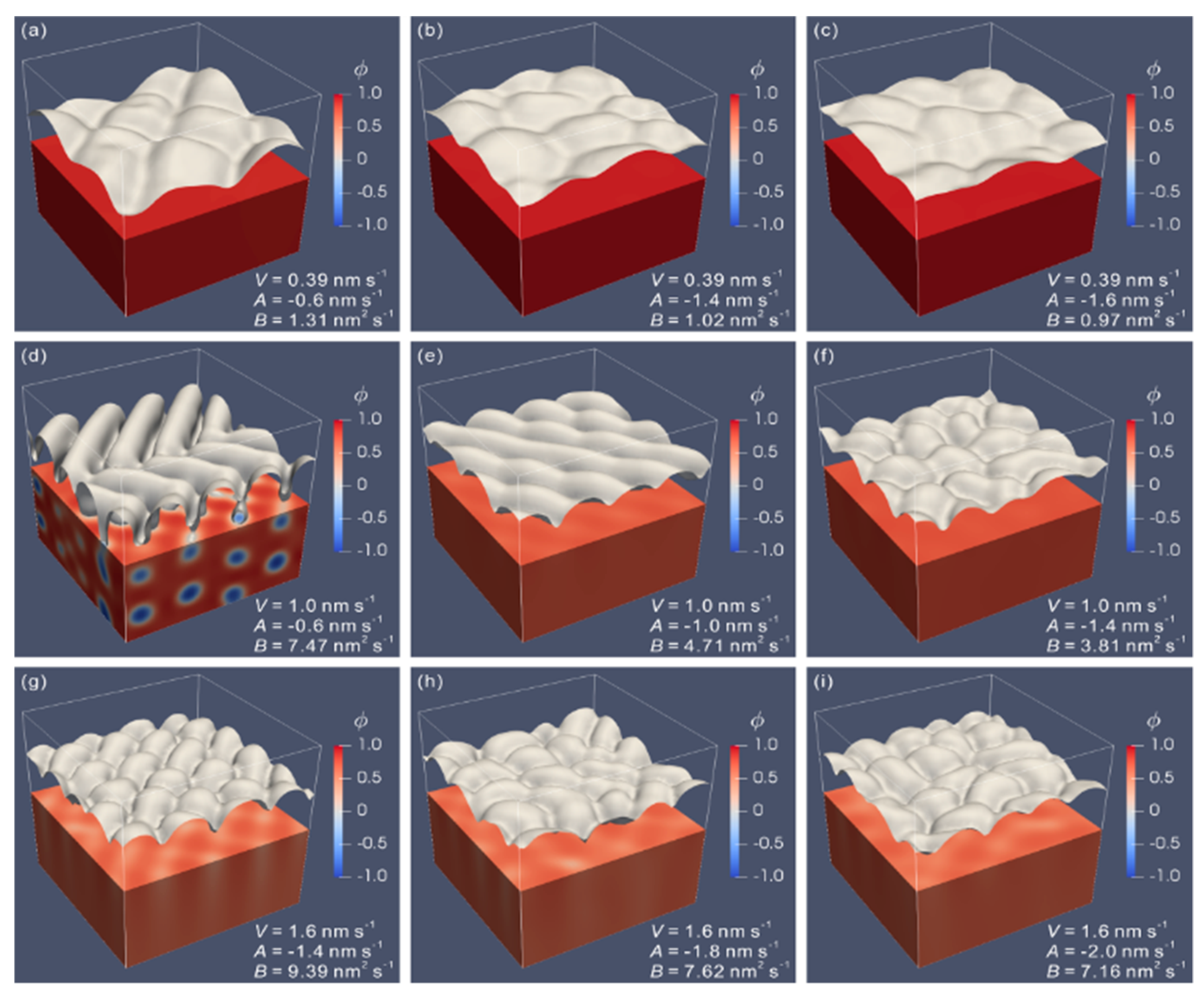
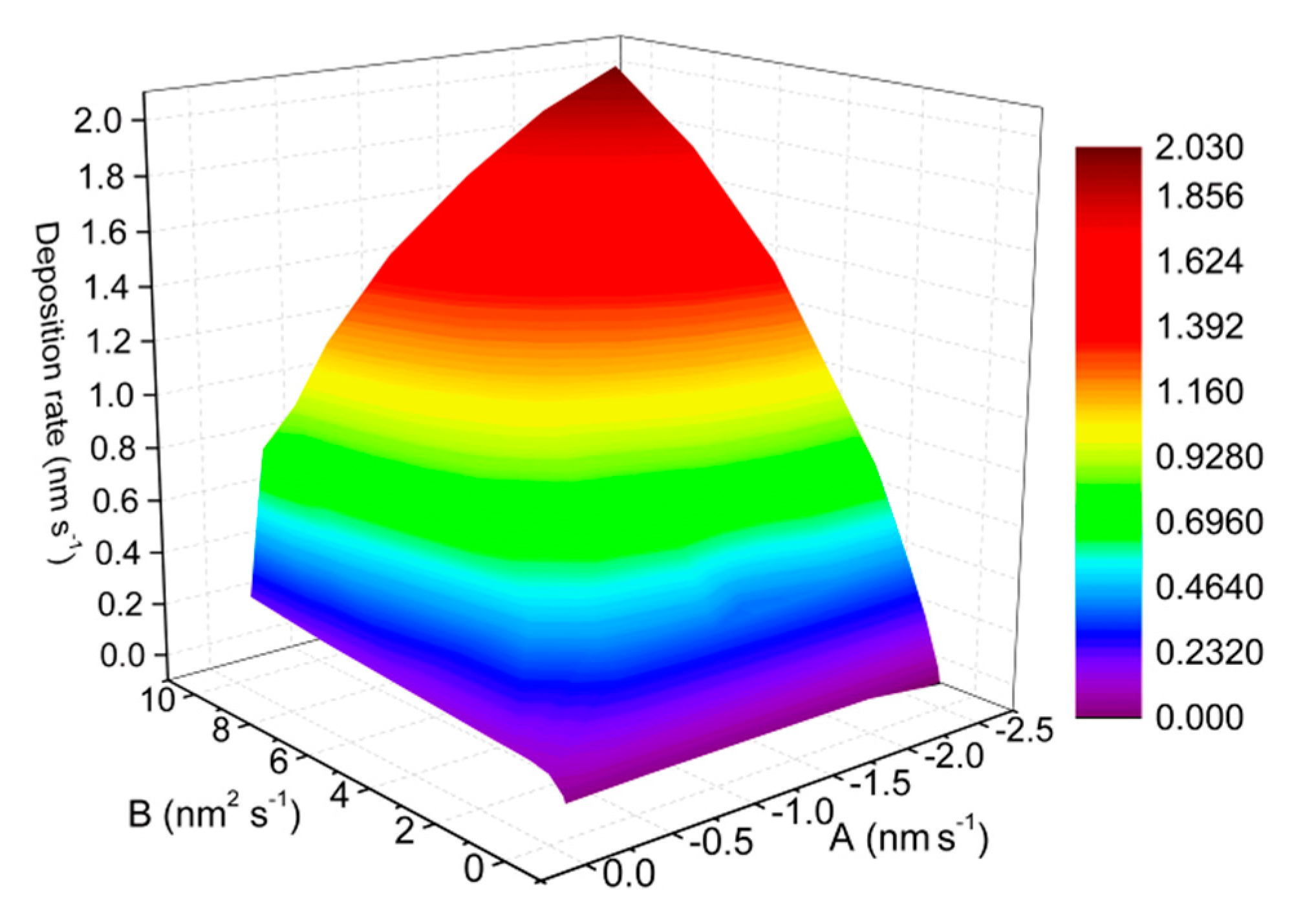
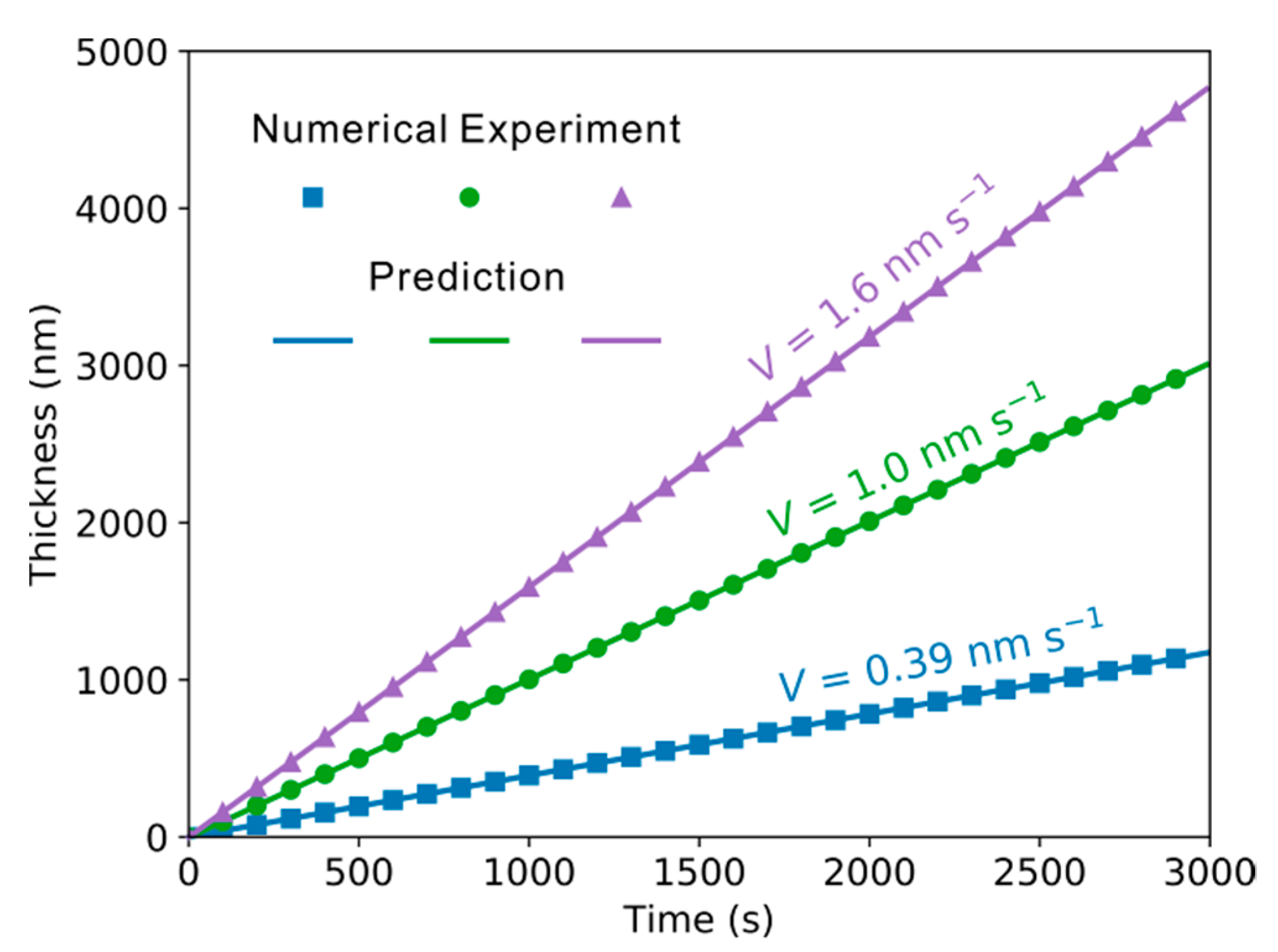
4.1. Relationship Between Deposition Rate and Model Parameters

The deposition rate of the thin films during the PVD process play an important role in controlling their properties. Extensive reports and discussions about the relationship between the deposition rate and the microstructure and surface morphologies of thin film are available. In this work, over 200 3D phase-field simulations for thin films during PVD were performed to obtain the relationship between the deposition rate and model parameters. Specifically, simulations were performed in a 3D domain of 48 × 48 × 48 grid points. The microstructures of the 3D simulations for thin films deposited with three different deposition rates (i.e., 0.39, 1.0, and 1.6 nm s−1) corresponding to the different gas–solid transition velocity and incident vapor rate at the deposition time of 10 min are displayed in Figure 1 for demonstration. As shown in Figure 1, the different gas–solid transition velocities and incident vapor rates corresponding to the same deposition rate result in different microstructures and surface topographies. The thin film deposited with a low deposition rate is denser than the one deposited with a high deposition rate. For the deposition rate of 0.39 nm s−1, the density of solid thin film does not significantly change with the gas–solid transition velocity and incident vapor rate. For the deposition rates of 1.0 and 1.6 nm s−1, the decreased incident vapor rate and the increased gas–solid transition velocity result in the thin film with lower density. Furthermore, there exist more columnar features of surface of the thin films with the higher deposition rate, especially for the thin film with higher gas–solid transition velocity (see Figure 1g).
Figure 2 displays the calculated deposition rates from the phase-field simulation results with different gas–solid transition velocities and incident vapor rates. As shown in Figure 2, the deposition rate decreases as the gas–solid transition velocity and incident vapor rate decrease. The deposition rate is relatively smaller and does not significantly change with the incident vapor rate when the gas–solid transition velocity is less than 1.0 nm2 s−1. Furthermore, it is obvious that the same deposition rate can be obtained through simulations with different sets of gas–solid transition velocities and incident vapor rates. For the same deposition rate, the required incident vapor rate is smaller when the gas–solid transition velocity is higher, whereas the required gas–solid transition velocity is smaller when the incident vapor rate is higher. Moreover, the deposition rates can be conveniently used to predict the temporal thin film thickness that are of interest in industry. The relationship between the thickness and deposition time due to the numerical simulations and the corresponding values predicted by the deposition rate are presented in Figure 3. As can be seen in the figure, both are in excellent agreement with each other.
The incident vapor rate provides the information on the amount of the vapor reaching the interface between gas and solid phase and the incident angle of the vapor. The gas-solid transition velocity is related to the characteristics of the film itself which is influenced by the deposition condition such as the gas pressure. The deposition rate is the efficient parameter usually used to characterize the properties of coatings. The deposition rate and parameterized model parameters including the incident vapor rate, gas-solid transition velocity and interfacial gradient coefficient can be compared to the control parameters in experiments, which realizes the correlation of the simulation results with the experimental data in the first step.

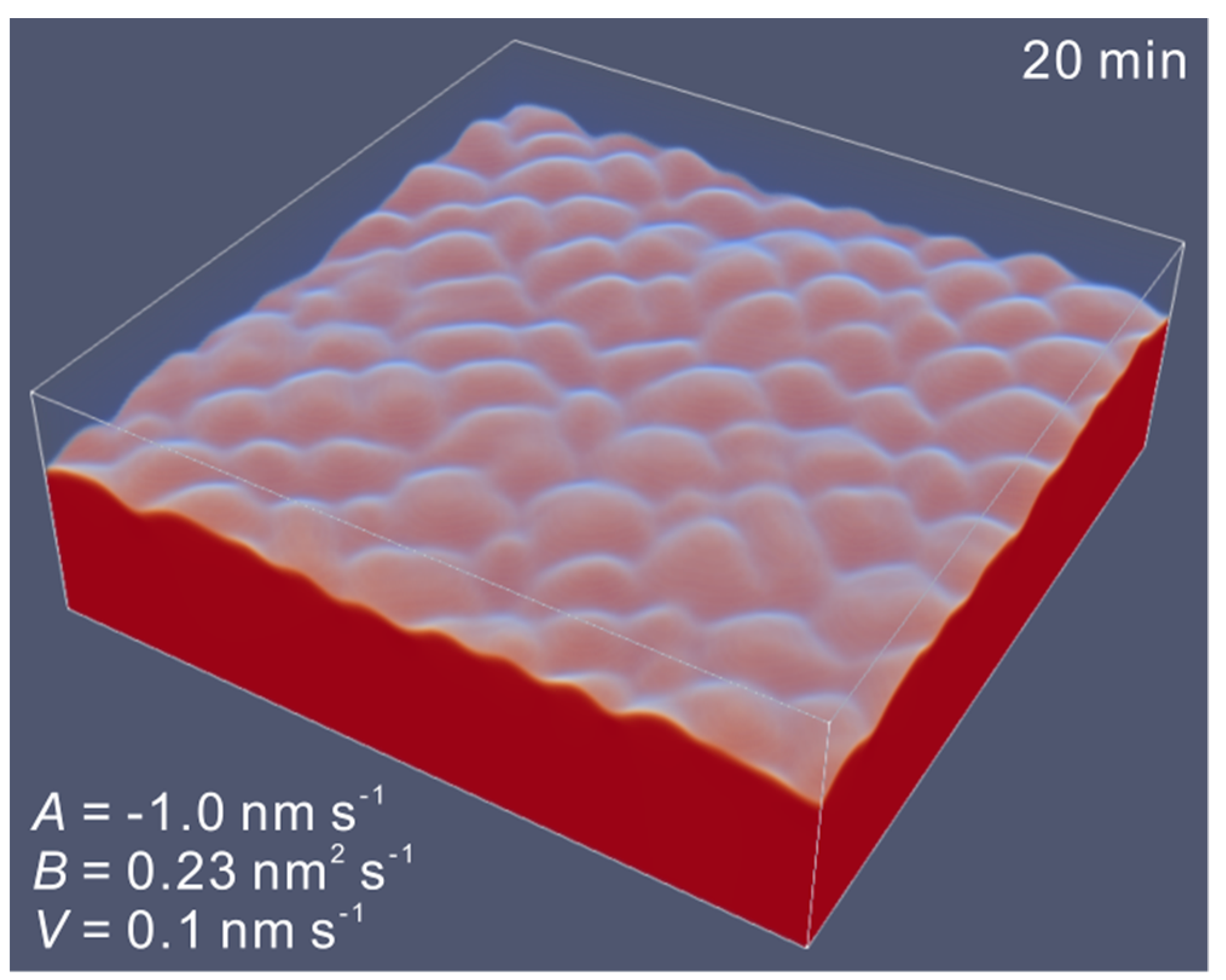
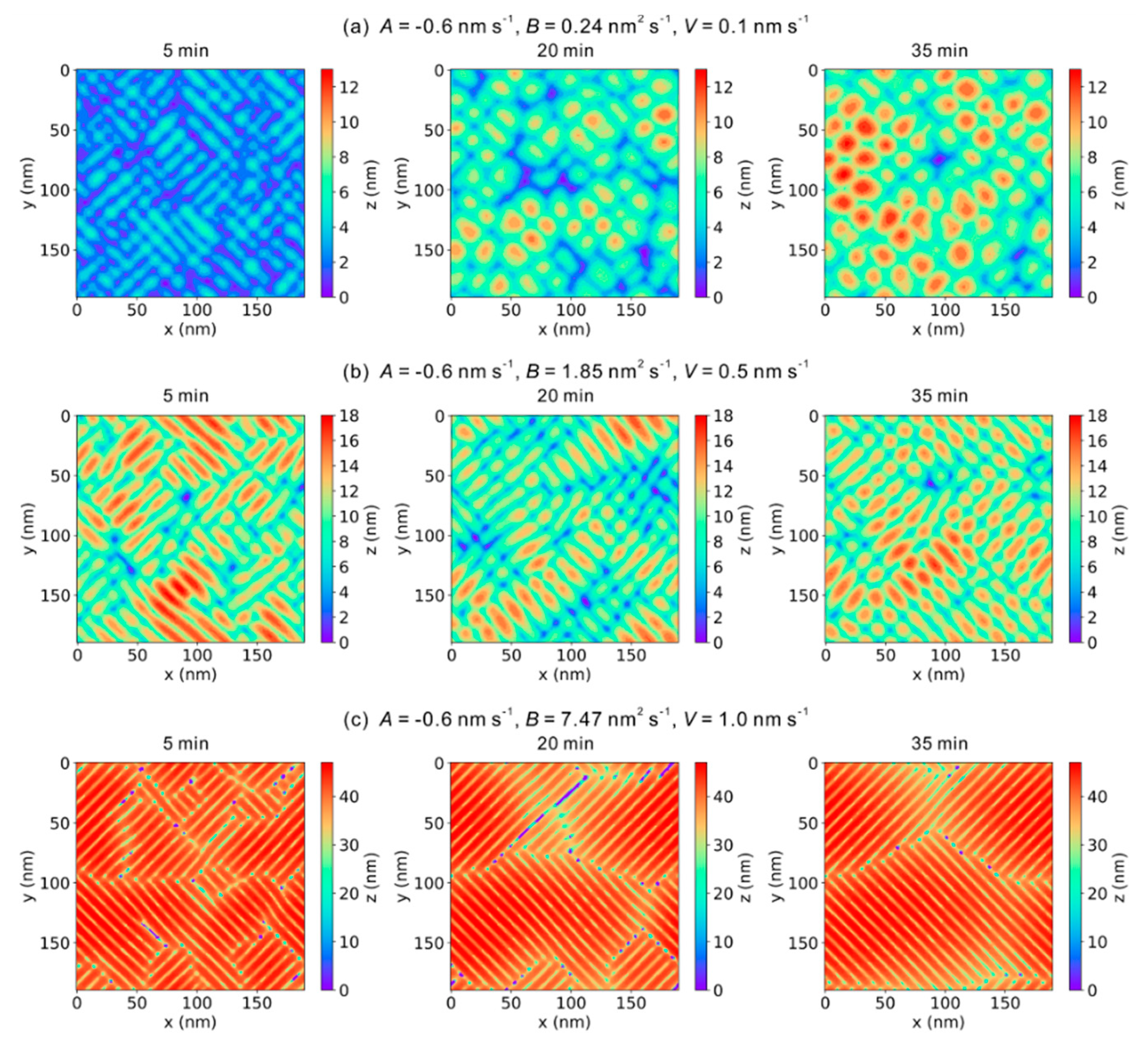
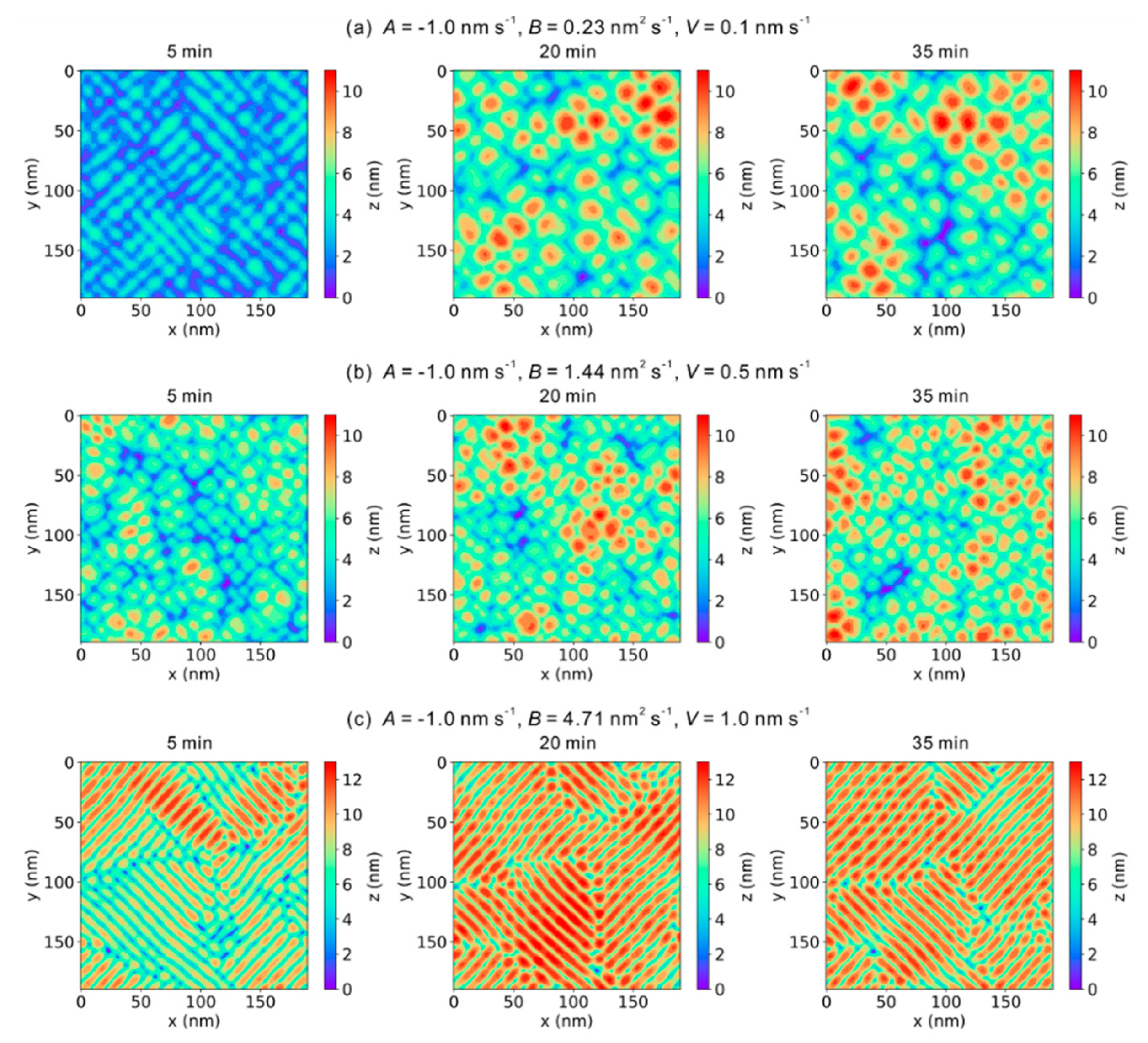
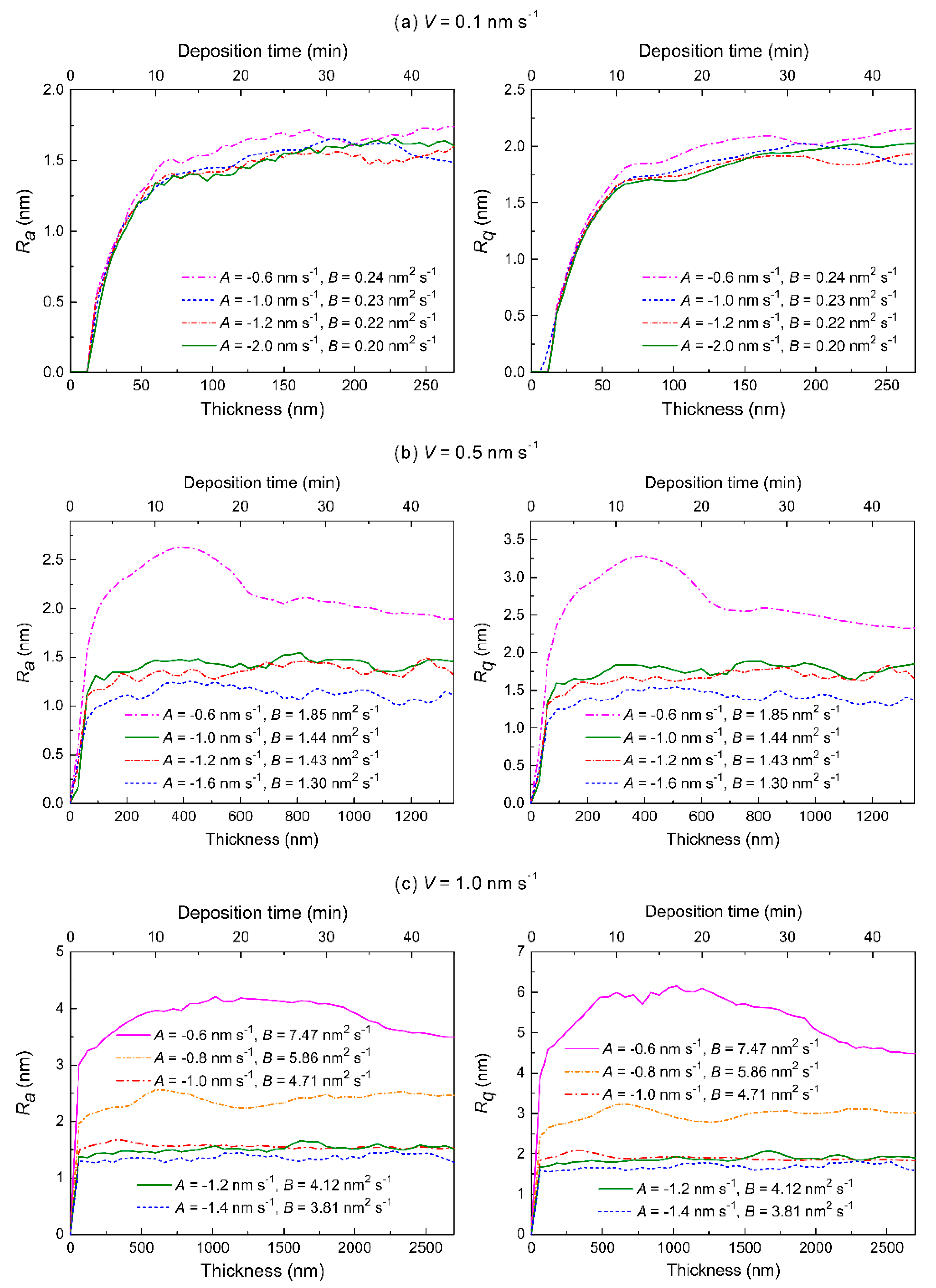
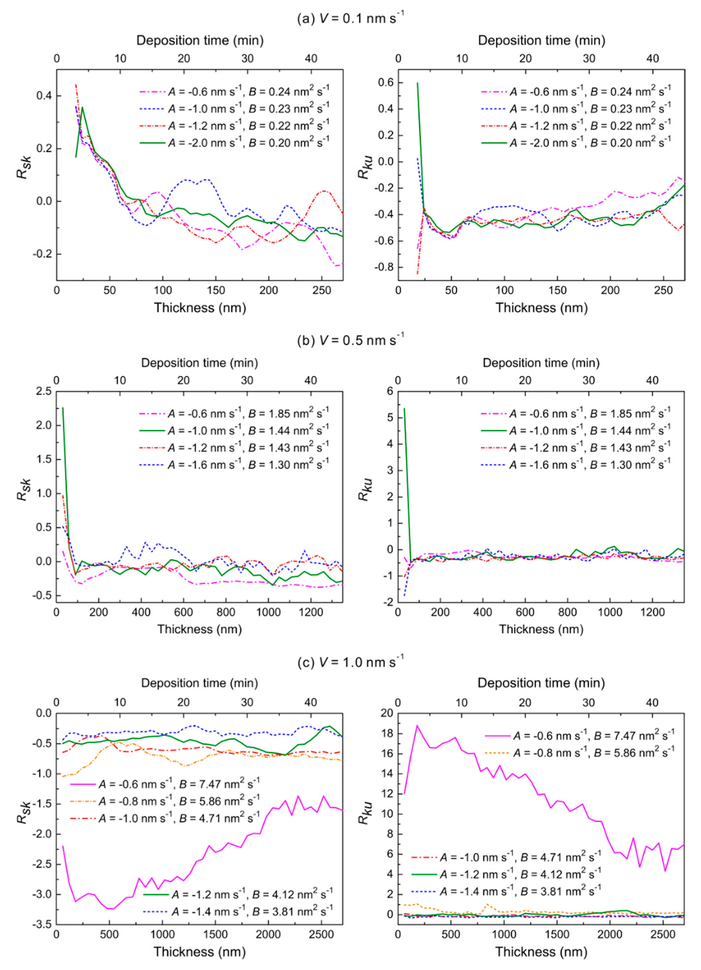
4.2. Effect of Deposition Rate and Time on Surface Roughness

The surface roughness commonly refers to the variations in the height of surface relative to a reference plane. The most commonly measured parameters for the roughness are the arithmetic average roughness (Ra) and root mean square roughness (Rq, also called RMS). Ra is the arithmetic mean of the absolute deviations between the height of the surface and the mean height of the surface, and Rq is the square root of the arithmetic mean of the square of deviations between the height of the surface and the mean height of the surface and is also used to calculate the skew and kurtosis parameters [38]. The mathematical forms of Ra and Rq are given as [2,38],
R a = 1 N x N y j = 1 N y i = 1 N x | Z i j μ |
R q = 1 N x N y j = 1 N y i = 1 N x ( Z i j μ ) 2
and
μ = 1 N x N y j = 1 N y i = 1 N x Z i j
where N x N y is the size for data sample, Zij is an array of relative heights of the surface in the x−y plane, and μ is the mean value of relative heights. Two other statistical height descriptors are skewness (Rsk) and kurtosis (Rku). Rsk is used to characterize the symmetry of the distribution for the variations of the surface heights relative to the mean height and is usually utilized to distinguish two profiles of the same Ra or Rq values but of different shapes. For distributions with dominating right tail, Rsk is positive, and thus peaks became dominant in the distribution, whereas for distributions with dominating left tail, Rsk is negative, and thus valleys become dominant in the distribution. Rku is a measurement of spikiness distribution profile. The surface is perfectly random if Rku = 3, spiky if Rku > 3, or bumpy for Rku < 3 [38]. Rsk and Rku are mathematically written as [2,39],
R s k = 1 N x N y R q 3 j = 1 N y i = 1 N x ( Z i j μ ) 3
R k u = 1 N x N y R q 4 j = 1 N y i = 1 N x ( Z i j μ ) 4 3
To systematically analyze surface roughness for thin films, several phase-field simulations with three different deposition rates of 0.1, 0.5, and 1.0 nm s−1 were performed in a larger 3D domain of 192 × 192 × 64 grid points. Figure 4 shows a typical 3D microstructure for the thin film due to the larger-size phase-field simulations with the deposition rate of 0.1 nm s−1 corresponding to the incident vapor rate of −1.0 nm s−1 and the gas–solid transition velocity of 0.23 nm2 s−1 at the deposition time of 20 min. The specific surface topography of thin films was further characterized according to their 3D simulated microstructures.
The heat maps of the surface height of thin films deposited with three different deposition rates of 0.1, 0.5, and 1.0 nm s−1 at three different deposition time of 5, 20, and 35 min are illustrated in Figure 5 and Figure 6, which are similar to the 2D atomic force microscopy (AFM) images used to analyze the surface roughness in the experimental investigation. As shown in Figure 5 and Figure 6, the surface heights of thin films with the deposition rate of 0.1 nm s−1 (see Figure 5a and Figure 6a) increase first as the deposition time increases from 5 to 20 min, but do not significantly change as the deposition time increases from 20 to 35 min. Moreover, there is no obvious difference in the surface heights of thin film with deposition rates of 0.5 nm s−1 (see Figure 5b and Figure 6b) and 1.0 nm s−1 (see Figure 5c and Figure 6c). This is because the growth of thin films with the deposition rate of 0.1 nm s-1 does not reach the steady state at the deposition time of 5 min, while the growth of thin films with deposition rates of 0.5 and 1.0 nm s−1 has reached the steady state at the deposition time of 5 min. Comparing Figure 5 with Figure 6, the surface heights of thin films with the incident vapor rate of −0.6 nm s−1 (see Figure 5) are higher than those of thin films with the incident vapor rate of −1.0 nm s−1 (see Figure 6) for the same deposition rate. For the deposition rate of 0.5 nm s−1 (see Figure 5b and Figure 6b), there exist same domains of the similar surface feature in the thin film with the incident vapor rate of −0.6 nm s−1 (see Figure 5b), but there is no such phenomenon in the thin films with the incident vapor rate of −1.0 nm s−1 (see Figure 6b). There are also some domains of the similar surface feature in thin films with the deposition rate of 1.0 nm s−1 (see Figure 5c and Figure 6c). Compared with the thin film with a deposition rate of 0.5 nm s−1 corresponding to the incident vapor rate of −0.6 nm s−1 (i.e., Figure 5b), there are wider domains of similar features in the thin films with the deposition rate of 1.0 nm s−1 (see Figure 5c and Figure 6c), especially for the thin film with the incident vapor rate of −0.6 nm s−1 (see Figure 5c). This is because there is not enough time to sufficiently diffuse and fluctuate for the vapor on the surface of the thin film, and there are a few vapors staying on the surface of thin film to further diffuse and fluctuate due to the large gas–solid transition velocity. There are a few vapors staying on the surface of thin film waiting to be deposited due to the large gas–solid transition velocity, which also causes the production of voids in thin films (see Figure 1d). From Figure 5c, it can be seen that domains of similar surface features become wider as the deposition time increases which is due to the continual incorporation of voids and columnar grains with the deposition time and shadowing effect.
The calculated surface roughness parameters due to the phase-field simulated thin films with the deposited thickness and deposition time are exhibited in Figure 7, Figure 8 and Figure 9. Figure 7 displays the values of Ra and Rq for thin films deposited at three different deposition rates of 0.1, 0.5, and 1.0 nm s−1 with the deposition thickness and deposition time. As shown in Figure 7, the values of Ra and Rq increase first as the deposited thickness and deposition time increase and then reach a steady state at the thickness of about 50 nm. The values of Ra and Rq of the thin films with larger deposition rates reach the steady state earlier than those with lower deposition rates, as confirmed in Figure 5 and Figure 6. Moreover, the values of Ra and Rq of thin films tend to increase as the deposition rate increases at the same incident vapor rate, whereas their values tend to decrease as the incident vapor rate increase for the same deposition rate. Figure 8 shows the ratio of Rq to Ra for thin films deposited at four different deposition rates of 0.1, 0.22, 0.5, and 1.0 nm s−1 with the deposition thickness and deposition time and also the comparison between ratios of Rq to Ra in the thin films with deposition rates of 0.22 and 1.0 nm s−1 due to the phase-field simulations and the experimental data in Mo and Ti thin films [2,3]. From Figure 8, it is found that most of the calculated ratios of Rq to Ra approach 1.31, suggesting that the distributions of surface heights approach a Gaussian distribution, which is in accordance with the report of Ref. [40]. Furthermore, the calculated ratios of Rq to Ra of thin films with deposition rates of 0.22 and 1.0 nm s−1 respectively agree well with the experimental data in Mo thin film by Aqil et al. [2] and Ti thin film by Lüdecke et al. [3]. Figure 9 exhibits the values of Rsk and Rku for thin films deposited at three different deposition rates of 0.1, 0.5, and 1.0 nm s−1 with the deposition thickness and deposition time. From Figure 9, it can be seen that most of the values of Rsk are negative, which indicates the valleys of most thin films due to the phase-field simulations, are dominant in the distribution. The values of Rsk of the thin film with the deposition rate of 1.0 nm s1, corresponding to the incident rate of −0.6 nm s−1 and gas–solid transition velocity of 7.47 nm2 s1, are negative and much smaller than the others, which indicates that there are a lot of very deep valleys in this thin film. The values of Rku of the thin films, except for the thin film with the deposition rate of 1.0 nm s1, corresponding to the incident rate of −0.6 nm s1 and gas–solid transition velocity of 7.47 nm2 s1 due to the phase-field simulation are smaller than 3, indicating their surfaces are bumpy. The values of Rku of the thin film with the deposition rate of 1.0 nm s1 corresponding to the incident rate of −0.6 nm s–1 and gas–solid transition velocity of 7.47 nm2 s1 are larger than 3, indicating its surface is spiky. As shown in Figure 7, Figure 8 and Figure 9, there are apparent differences in the calculated roughness parameters between the thin film with the deposition rate of 1.0 nm s1 corresponding to the incident rate of −0.6 nm s−1 and gas–solid transition velocity of 7.47 nm2 s1 and the others. That is because the valleys of the surface in the thin film with the deposition rate of 1.0 nm s1 corresponding to the incident rate of −0.6 nm s1 and gas–solid transition velocity of 7.47 nm2 s1 are very deep and their peaks are quite spiky because of the well-known shadow effects. Such deep valleys of the surface in the thin film will evolve to voids as the deposition time increases.

5. Further Discussion on the Relationship between Surface Roughness and Density

The surface roughness and density are two effective quantities for characterizing the properties of the microstructure and surface morphologies of the deposited thin films, which significantly affect their service performance. On the basis of the results in Section 4, it can be found that the model parameters, including the incident vapor rate and gas–solid transition velocity, show a profound impact on the phase-field simulated microstructure and surface morphologies during the PVD process. Specifically, the model parameters as well as the deposition rate tend to conjointly shape the microstructure and surface morphologies of the deposited thin film. Further insight into such cooperative effects can be indicated from the correlation between surface roughness and density of thin film, based on the comprehensive comparison among the microstructures in Figure 1, the surface morphologies in Figure 5 and Figure 6, and the calculated roughness parameters in Figure 7, Figure 8 and Figure 9. As shown in Figure 1, the thin film with the higher deposition rate corresponding to the lower incident rate and higher gas–solid transition velocity usually possesses the lower density. From Figure 5, Figure 6 and Figure 7, it can be found that the thin film with the higher deposition rate corresponding to the lower incident rate and higher gas–solid transition velocity possesses higher roughness. Comparing Figure 1d,e with Figure 5c, Figure 6c, and Figure 7c, the thin film with the higher roughness possesses the lower density because when the surface roughness is large enough, some parts of the interface are shadowed and hence do not grow. The shadowing effect is more obvious for thin films with the deep valleys (i.e., the values of Rsk of the thin film are negative and smaller) and very spiky surface (i.e., the values of Rku of the thin film with higher roughness are larger than three or even higher). There are a few incident vapors reaching deep valleys, especially for the thin film with higher gas–solid transition velocity, where there are a few vapors on surface to be deposited and further sufficiently diffuse. There exist massive voids in the thin film at deposition rate of 1.0 nm s−1 corresponding to the incident vapor rate of −0.6 nm s−1 and gas–solid transition velocity of 7.47 nm2 s−1 (see Figure 1d) and its roughness is also very large (see Figure 6c and Figure 7c), which confirms the presently proposed relationship between the surface roughness and the density.

6. Conclusions

  • In this paper, more than 200 sets of 3D phase-field simulations of the PVD process of metal thin films were performed based on the parameterized phase-field model by Keblinski et al. A quantitative relationship between model parameters and deposition rates at steady state was established.
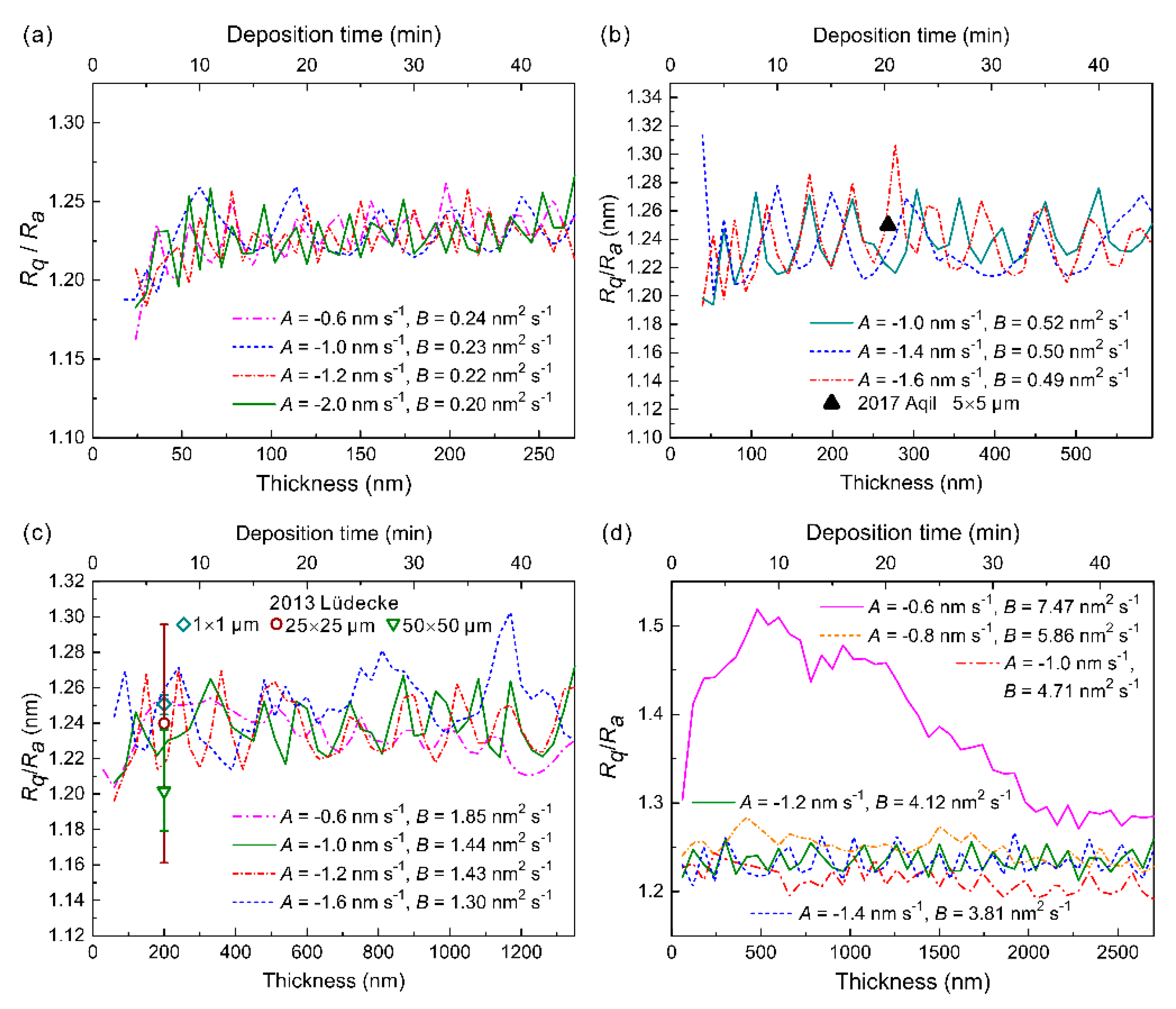
  • Insight into the relationship among the industrially concerned properties, i.e., deposition rates, surface roughness and density, and the microstructures and surface morphologies of the metal thin films was further investigated by conducting 3D phase-field simulations with larger domain. Relationship between the surface roughness and the deposition rate is proven to be in accordance with the common sense in experiments, i.e., that the higher deposition rate generally leads to the higher surface roughness. Specially, the calculated ratios of Rq to Ra of metal thin films with deposition rates of 0.22 and 1.0 nm s−1 are in very good agreement with the experimental data of the deposited Mo and Ti thin films.
  • Delicate elaboration over the formation of voids and the relation between the density and roughness was acquired by carefully associating the relation among different control parameters. It was found that the metal thin films with the higher roughness usually possess the lower density. Furthermore, the present results reveal the potential difficulties in the PVD process as the control parameters tend to affect the properties of thin films conjointly.
  • With the present quantitative phase-field simulations, the relationship between the control parameters and microstructures and properties of the deposited thin films can be efficiently established, which is anticipated to be used for precisely guiding the manufacture of thin films with the desired properties by means of the PVD technique.

Author Contributions

Conceptualization, L.Z. and M.C.; methodology and code, S.Y. and J.Z.; validation, S.Y., J.Z., and L.Z.; writing—original draft preparation, S.Y. and J.Z.; writing—review and editing, J.Z. and L.Z.; project administration, M.C. and L.Z.

Funding

This research was funded by the National MCF Energy R & D Program of China, grant number 2018YFE0306100, and the Director Foundation of China Academy of Engineering Physics, grant number YZ2015009.

Conflicts of Interest

The authors declare no conflict of interest.

References

  1. Chan, K.Y.; Tou, T.Y.; Teo, B.-S. Effects of substrate temperature on electrical and structural properties of copper thin films. Microelectron. J. 2006, 37, 930–937. [Google Scholar] [CrossRef]
  2. Aqil, M.M.; Azam, M.A.; Aziz, M.F.; Latif, R. Deposition and characterization of molybdenum thin film using direct current magnetron and atomic force microscopy. J. Nanotechnol. 2017, 2017, 4862087. [Google Scholar] [CrossRef]
  3. Lüdecke, C.; Bossert, J.; Roth, M.; Jandt, K.D. Physical vapor deposited titanium thin films for biomedical applications: Reproducibility of nanoscale surface roughness and microbial adhesion properties. Appl. Surf. Sci. 2013, 280, 578–589. [Google Scholar] [CrossRef]
  4. Singh, A.; Kuppusami, P.; Thirumurugesan, R.; Ramaseshan, R.; Kamruddin, M.; Dash, S.; Ganesan, V.; Mohandas, E. Study of microstructure and nanomechanical properties of Zr films prepared by pulsed magnetron sputtering. Appl. Surf. Sci. 2011, 257, 9909–9914. [Google Scholar] [CrossRef]
  5. Li, C.; Guo, H.; Gao, L.; Wei, L.; Gong, S.; Xu, H. Microstructures of yttria-stabilized zirconia coatings by plasma spray-physical vapor deposition. J. Therm. Spray Technol. 2015, 24, 534–541. [Google Scholar] [CrossRef]
  6. Ta, N.; Zhang, L.; Tang, Y.; Chen, W.; Du, Y. Effect of temperature gradient on microstructure evolution in Ni–Al–Cr bond coat/substrate systems: A phase-field study. Surf. Coat. Technol. 2015, 261, 364–374. [Google Scholar] [CrossRef]
  7. Ta, N.; Zhang, L.; Du, Y. A trial to design γ/γ′ bond coat in Ni–Al–Cr Mode TBCs Aided by Phase-Field Simulation. Coatings 2018, 8, 421. [Google Scholar] [CrossRef]
  8. Zhou, J.; Zhong, J.; Chen, L.; Zhang, L.; Du, Y.; Liu, Z.-K.; Mayrhofer, P.H. Phase equilibria, thermodynamics and microstructure simulation of metastable spinodal decomposition in c–Ti1− xAlxN coatings. Calphad 2017, 56, 92–101. [Google Scholar] [CrossRef]
  9. Grigoriev, S.; Vereschaka, A.; Metel, A.; Sitnikov, N.; Milovich, F.; Andreev, N.; Shevchenko, S.; Rozhkova, Y. Investigation into Performance of multilayer composite nano-structured Cr-CrN-(Cr0.35Ti0.40Al0.25) N coating for metal cutting tools. Coatings 2018, 8, 447. [Google Scholar] [CrossRef]
  10. Bujak, J.; Walkowicz, J.; Kusiński, J. Influence of the nitrogen pressure on the structure and properties of (Ti, Al) N coatings deposited by cathodic vacuum arc PVD process. Surf. Coat. Technol. 2004, 180, 150–157. [Google Scholar] [CrossRef]
  11. Kazmanli, M.; Ürgen, M.; Cakir, A. Effect of nitrogen pressure, bias voltage and substrate temperature on the phase structure of Mo–N coatings produced by cathodic arc PVD. Surf. Coat. Technol. 2003, 167, 77–82. [Google Scholar] [CrossRef]
  12. Ahlgren, M.; Blomqvist, H. Influence of bias variation on residual stress and texture in TiAlN PVD coatings. Surf. Coat. Technol. 2005, 200, 157–160. [Google Scholar] [CrossRef]
  13. Sprute, T.; Tillmann, W.; Grisales, D.; Selvadurai, U.; Fischer, G. Influence of substrate pre-treatments on residual stresses and tribo-mechanical properties of TiAlN-based PVD coatings. Surf. Coat. Technol. 2014, 260, 369–379. [Google Scholar] [CrossRef]
  14. Nastac, L.; Dong, H.; Dax, F.R.; Hanusiak, W. The CFD modeling of the EB-PVD of SiC/Ti-6Al-4V coatings. JOM 2004, 56, 49–53. [Google Scholar] [CrossRef]
  15. Adebiyi, D.; Popoola, A.; Botef, I. Experimental verification of statistically optimized parameters for low-pressure cold spray coating of titanium. Metals 2016, 6, 135. [Google Scholar] [CrossRef]
  16. Kapopara, J.M.; Mengar, A.R.; Chauhan, K.V.; Rawal, S.K. CFD analysis of sputtered TiN coating. Mater. Today Proc. 2017, 4, 9390–9393. [Google Scholar] [CrossRef]
  17. Pinto, G.; Silva, F.; Porteiro, J.; Mínguez, J.; Baptista, A. Numerical simulation applied to PVD reactors: An overview. Coatings 2018, 8, 410. [Google Scholar] [CrossRef]
  18. Raghavan, S.; Mayo, M.J.; Wang, H.; Dinwiddie, R.B.; Porter, W.D. The effect of grain size, porosity and yttria content on the thermal conductivity of nanocrystalline zirconia. Scr. Mater. 1998, 39, 1119–1125. [Google Scholar] [CrossRef]
  19. Mayrhofer, P.H.; Tischler, G.; Mitterer, C. Microstructure and mechanical/thermal properties of Cr–N coatings deposited by reactive unbalanced magnetron sputtering. Surf. Coat. Technol. 2001, 142, 78–84. [Google Scholar] [CrossRef]
  20. Kulkarni, A.; Vaidya, A.; Goland, A.; Sampath, S.; Herman, H. Processing effects on porosity-property correlations in plasma sprayed yttria-stabilized zirconia coatings. Mater. Sci. Eng. A 2003, 359, 100–111. [Google Scholar] [CrossRef]
  21. Mayrhofer, P.; Mitterer, C.; Musil, J. Structure–property relationships in single-and dual-phase nanocrystalline hard coatings. Surf. Coat. Technol. 2003, 174, 725–731. [Google Scholar]
  22. Zhang, C.X.; Liu, F.S.; Gong, S.K.; Xu, H.B. Characterization and evaluation of EB-PVD thermal barrier coatings by impedance spectroscopy. Mater. Sci. Forum 2005, 475–479, 3997–4000. [Google Scholar]
  23. Jang, B.-K.; Matsubara, H. Influence of porosity on thermophysical properties of nano-porous zirconia coatings grown by electron beam-physical vapor deposition. Scr. Mater. 2006, 54, 1655–1659. [Google Scholar] [CrossRef]
  24. Sohn, Y.; Biederman, R.; Sisson, R., Jr. Microstructural development in physical vapour-deposited partially stabilized zirconia thermal barrier coatings. Thin Solid Films 1994, 250, 1–7. [Google Scholar]
  25. Schulz, U.; Schmücker, M. Microstructure of ZrO2 thermal barrier coatings applied by EB-PVD. Mater. Sci. Eng. A 2000, 276, 1–8. [Google Scholar] [CrossRef]
  26. Yang, Y.; Johnson, R.; Wadley, H. A Monte Carlo simulation of the physical vapor deposition of nickel. Acta Mater. 1997, 45, 1455–1468. [Google Scholar]
  27. Zhang, J.; Adams, J.B. Modeling and visualization of polycrystalline thin film growth. Comput. Mater. Sci. 2004, 31, 317–328. [Google Scholar] [CrossRef]
  28. Cho, J.; Terry, S.; LeSar, R.; Levi, C. A kinetic Monte Carlo simulation of film growth by physical vapor deposition on rotating substrates. Mater. Sci. Eng. A 2005, 391, 390–401. [Google Scholar] [CrossRef]
  29. Wang, P.; He, W.; Mauer, G.; Mücke, R.; Vaßen, R. Monte Carlo simulation of column growth in plasma spray physical vapor deposition process. Surf. Coat. Technol. 2018, 335, 188–197. [Google Scholar] [CrossRef]
  30. Wang, Z.; Zhang, D.; Ke, P.; Liu, X.; Wang, A. Influence of substrate negative bias on structure and properties of TiN coatings prepared by hybrid HIPIMS method. J. Mater. Sci. Technol. 2015, 31, 37–42. [Google Scholar]
  31. Raoufi, D.; Kiasatpour, A.; Fallah, H.R.; Rozatian, A.S.H. Surface characterization and microstructure of ITO thin films at different annealing temperatures. Appl. Surf. Sci. 2007, 253, 9085–9090. [Google Scholar] [CrossRef]
  32. Huang, Y.; Lü, X.; Jing, W.M.; Huang, N. In vitro investigation of protein adsorption and platelet adhesion on inorganic biomaterial surfaces. Appl. Surf. Sci. 2008, 255, 257–259. [Google Scholar] [CrossRef]
  33. Puckett, S.D.; Taylor, E.; Raimondo, T.; Webster, T.J. The relationship between the nanostructure of titanium surfaces and bacterial attachment. Biomaterials 2010, 31, 706–713. [Google Scholar] [CrossRef] [PubMed]
  34. Keblinski, P.; Maritan, A.; Toigo, F.; Messier, R.; Banavar, J.R. Continuum model for the growth of interfaces. Phys. Rev. E 1996, 53, 759. [Google Scholar] [CrossRef] [PubMed]
  35. Warren, J.A.; Kobayashi, R.; Lobkovsky, A.E.; Carter, W.C. Extending phase-field models of solidification to polycrystalline materials. Acta Mater. 2003, 51, 6035–6058. [Google Scholar] [CrossRef]
  36. Stewart, J.A.; Spearot, D.E. Phase-field models for simulating physical vapor deposition and grain evolution of isotropic single-phase polycrystalline thin films. Comput. Mater. Sci. 2016, 123, 111–120. [Google Scholar] [CrossRef] [Green Version]
  37. Stewart, J.A.; Spearot, D.E. Phase-field simulations of microstructure evolution during physical vapor deposition of single-phase thin films. Comput. Mater. Sci. 2017, 131, 170–177. [Google Scholar] [CrossRef]
  38. Bhushan, B. Surface roughness analysis and measurement techniques. In Modern Tribology Handbook, Two Volume Set, 1st ed.; CRC press: Boca Raton, FL, USA, 2000; pp. 79–150. [Google Scholar]
  39. Kumar, B.R.; Rao, T.S. AFM Studies on surface morphology, topography and texture of nanostructured zinc aluminum oxide thin films. Dig. J. Nanomater. Bios. 2012, 7, 1881–1889. [Google Scholar]
  40. Thomas, T.R. Rough Surfaces, 2nd ed.; Imperial College Press: London, UK, 1999; pp. 133–150. [Google Scholar]
Figure 1. Typical microstructures due to the 3D phase-field simulations performed in a domain with 48 × 48 × 48 nm3 for thin films deposited with three different deposition rates (denoted as V) corresponding to the different gas-solid transition velocities (denoted as A) and incident vapor rates (denoted as B) at the deposition time of 10 min: (a) V = 0.39 nm s−1, A = −0.6 nm s−1 and B = 1.32 nm2 s−1, (b) V = 0.39 nm s−1, A = −1.4 nm s−1 and B = 1.02 nm2 s−1 , (c) V = 0.39 nm s−1, A = −1.6 nm s−1 and B = 0.97 nm2 s−1, (d) V = 1.0 nm s−1, A = −0.6 nm s−1 and B = 7.47 nm2 s−1, (e) V = 1.0 nm s−1, A = −1.0 nm s−1 and B = 4.71 nm2 s−1, (f) V = 1.0 nm s−1, A = −1.4 nm s−1 and B = 3.81 nm2 s−1, (g) V = 1.6 nm s−1, A = −1.4 nm s−1 and B = 9.39 nm2 s−1, (h) V = 1.6 nm s−1, A = −1.8 nm s−1 and B = 7.62 nm2 s−1 and (i) V = 1.6 nm s−1, A = −2.0 nm s−1 and B = 7.16 nm2 s−1.
Coatings 09 00607 g001
Figure 2. Calculated deposition rates based on the phase-field simulation results with different gas–solid transition velocities (i.e., B) and incident vapor rates (i.e., A). Here, the negative sign in front of values of A only represents the direction.
Coatings 09 00607 g002
Figure 3. Comparison between the temporal thickness of thin films deposited with the deposition rates of 0.39, 1.0, and 1.6 nm s−1 due to the phase-field simulations and the corresponding results predicted by the deposition rate. Symbols denote the phase-field simulated results, while solid lines denote the predicted results based on the pre-set deposition rates.
Coatings 09 00607 g003
Figure 4. A typical microstructure due to the 3D phase-field simulation performed in a domain with 192 × 192 × 64 nm3 for thin films deposited with the deposition rates of 0.1 nm s−1 corresponding to the incident vapor rate of −1.0 nm s−1 and the gas–solid transition velocity of 0.23 nm2 s−1 at the deposition time of 20 min.
Coatings 09 00607 g004
Figure 5. Heat maps of the surface height of thin films deposited with three different deposition rates corresponding to the incident vapor rate fixed as −0.6 nm s−1 and three different gas-solid transition velocities at three different deposition time of 5, 20 and 35 min due to the phase-field simulations.
Coatings 09 00607 g005
Figure 6. Heat maps of the surface height of thin films deposited with three different deposition rates corresponding to the incident vapor rate fixed as −1.0 nm s−1 and three different gas-solid transition velocities at three different deposition time of 5, 20 and 35 min due to the phase-field simulations.
Coatings 09 00607 g006
Figure 7. Values of Ra and Rq for thin films deposited at three different deposition rates of (a) 0.1 nm s−1, (b) 0.5 nm s−1, and (c) 1.0 nm s−1 with the corresponding deposition thickness and time.
Coatings 09 00607 g007
Figure 8. Ratios of Rq to Ra for thin films deposited at four different deposition rates of (a) 0.1 nm s−1, (b) 0.22 nm s−1, (c) 0.5 nm s−1, and (d) 1.0 nm s−1 with the deposition thickness and deposition time, compared with the experimental data [2,3].
Coatings 09 00607 g008
Figure 9. Values of Rsk and Rku for thin films deposited at three different deposition rates of (a) 0.1 nm s−1, (b) 0.5 nm s−1, and (c) 1.0 nm s−1 with the corresponding deposition thickness and deposition time.
Coatings 09 00607 g009
Table 1. List of the model and numerical parameters used in the present phase-field simulations.
ParametersSymbolsValues
Grid spacingΔx1.0 nm
Interfacial gradient coefficienta0.5 J m2
Noise amplitudeC2.5 J m−1
Gaussian noise factorη0.5
Supplied incident vaporg01.0

