Article

Relationship Processing–Composition–Structure–Resistivity of LaNiO3 Thin Films Grown by Chemical Vapor Deposition Methods

1
FEMTO-ST Institute, University of Bourgogne Franche-Comté, CNRS (UMR 6174), ENSMM, 26 rue de l’Epitaphe, 25030 Besançon, France
2
Faculty of Chemistry and Geosciences, Vilnius University, Naugarduko 24, 03225 Vilnius, Lithuania
3
Annealsys, 139 rue des Walkyries, 34000 Montpellier, France
4
Jean Lamour Institute, CNRS (UMR 7198), Université de Lorraine, 2 allée André Guinier, 54011 Nancy, France
*
Author to whom correspondence should be addressed.
Coatings 2019, 9(1), 35; https://doi.org/10.3390/coatings9010035
Submission received: 21 September 2018 / Revised: 22 December 2018 / Accepted: 27 December 2018 / Published: 10 January 2019
(This article belongs to the Special Issue Chemical Vapor Deposition 2018)

Abstract

:
Precision control of resistivity/conductivity of LaNiO3 (LNO) films is essential for their integration as electrodes in the functional heterostructures. This becomes possible if the relationship between processing parameters–composition–structure–resistivity is determined. LaNiO3 films were deposited by three different chemical vapor deposition methods using different precursor supply systems: direct liquid delivery, pulsed liquid injection, and aerosol generation. The possibilities to ameliorate the efficiency of precursor evaporation and of film growth were studied. The relationship between deposition conditions and composition was determined. Detailed analysis of the epitaxial growth of LNO films on cubic and trigonal substrates and the influence of the rhombohedral distortion on the microstructural quality was done. The resistivity of LaNiO3 films, grown by chemical vapor deposition, was mainly defined by microstructural defects and La/Ni composition. The high epitaxial quality LaNiO3/LaAlO3 films with nearly stoichiometric La/Ni ratio presented low resistivity, which was very close to that of bulk LaNiO3. Their annealing in oxygen atmosphere had little effect on the resistivity, which suggests a minor presence of oxygen vacancies in the as-grown films.

Graphical Abstract

1. Introduction

Research on conductive oxides exhibiting a perovskite-type ABO3 structure, e.g., SrRuO3 (SRO), LaNiO3 (LNO), or (LaxBa1−x)SnO3 are widely studied due to the fact that they could be employed as bottom electrodes and greatly improve the aging and the fatigue of ferroelectric memories [1]. In this family, LNO is a paramagnetic and metallic oxide down to 1.5 K and its bulk resistivity value is around 2.5 mΩ cm at room temperature [2,3]. LNO has a trigonal structure, which can be described by the hexagonal cell with a = 5.454 Å, c = 13.106 Å, and γ = 120° or rhombohedral cell with parameters a = 5.385 Å and α = 60.84° [4]. The LNO lattice parameters fit well with many functional perovskite materials such as SrTiO3 (STO), LaAlO3 (LAO), BaTiO3, Pb(Zr,Ti)O3 (PZT), etc. The LNO films were widely studied as a bottom electrode and as a seed layer for the growth of highly (100)-oriented PZT films for applications in actuators and energy harvesters [5,6]. The deposition of artificial LNO/LAO superlattices has been investigated for next generation devices [7,8] as well. Mainly, the (01 1 ¯ 2) growth orientation of hexagonal cell ((100) orientation in pseudo-cubic settings) has been reported. Although, the epitaxial LNO growth on cubic and pseudo-cubic substrates such as STO and LAO is well known in literature and the description of the LNO structure is usually completed by using a simplified pseudo-cubic cell. It is important to note that LNO is not a cubic but trigonal material and its physical and structural properties are not isotropic.
LNO films have been deposited by several different physical and chemical deposition methods including a pulsed laser deposition (PLD) [9,10], metalorganic decomposition (MOD) [11], sputtering [12], metalorganic chemical vapor deposition (MOCVD), and atomic layer deposition (ALD) [13,14,15]. However, as Ni3+ is not the most stable oxidation state of nickel, deposited films often contained a mixture of Ni3+ and Ni2+ ions, which then led to the formation of oxygen vacancies in the structure heavily impacting the conductivity of the layer [16]. Although, the relationship between oxygen non-stoichiometry and conductivity/resistivity of LNO layers was widely investigated, the effect of La/Ni ratio on LNO film properties remains little studied [13]. This can be explained by the fact that tuning of the film composition demands the change of the target in physical methods and, thus, stoichiometric targets are usually considered if the deposited materials do not have volatile components. The CVD methods offer a possibility to investigate easily the relationship between the film composition and the physical properties of deposited films.
Different types of La and Ni precursors including bimetallic precursors were tested for the growth of LNO films by means of MOCVD [17]. La and Ni β-diketonates (Ni(tmhd)2 and La(tmhd)3, where tmhd stands for 2,2,6,6-tetramethyl-3,5-heptadionato) remain to be the most frequently used ones [13,18,19,20]. Although, the thermogravimetric analysis for these two precursors can be found in the literature [19,21,22], their thermal decomposition was less studied. The evaporation temperatures for MOCVD processes were most of the time chosen arbitrarily and without detailed optimization. Thus, there is a strong disagreement in the literature regarding the relationship between the La/Ni ratio and the film composition [13,22].
The precursors delivery principle and conditions may considerably influence the deposition process and film composition, especially in the case of the deposition of multi-component oxide layers. Therefore, in this paper, in order to optimize the composition and the growth efficiency of LNO films from La and Ni β-diketonates by CVD techniques, the effects of solvent, evaporation temperature, deposition pressure, growth temperature, and relationship between compositions of film and solution have been studied by using CVD reactors with three different precursor delivery systems. (01 1 ¯ 2) LNO films were grown epitaxially on pseudo-cubic (trigonal) and cubic substrates. The relationship between the microstructure and resistivity of LNO films is discussed.

2. Materials and Methods

LaNiO3 thin films were grown on (01 1 ¯ 2) R-sapphire, (100) Si, and (01 1 ¯ 2) LaAlO3 substrates by three different metal organic chemical vapor deposition (MOCVD) methods: pulsed injection (PI) MOCVD [23,24], atmospheric pressure (AP) MOCVD [25], and commercial direct liquid injection (DLI) MOCVD (annealsys MC-100) [26,27]. The schematic representations of the used PIMOCVD, APMOCVD, and DLI-CVD reactors can be found in [22,28,29], respectively. In the case of DLI-CVD, prior to depositions, the substrates were cleaned in acetone and piranha solution (H2SO4 + H2O2), rinsed in deionized water, and then dried under N2 gas flow. Prior to PIMOCVD and APMOCVD processes, the substrates were cleaned in toluene (heated up to 110 °C), rinsed in acetone and ethanol, and dried under N2 gas flow. The deposition conditions used in three methods are summarized in Table 1. In the case of the PIMOCVD or DLI-CVD, micro-doses of a solution of metalorganic precursors were injected with a defined frequency into a hot evaporator where they quickly evaporated. A single liquid injector line was used to introduce a solution of La and Ni precursor mixture in PIMOCVD, while two new two-stage mist injection systems, plugged on the same vaporizer body, were used to introduce separately the La and Ni solution in the DLI-CVD tool. An aerosol of precursor solution, generated by an ultrasound, was transported by carrier gasses at ambient conditions to the heated substrates in APMOCVD. Anhydrous 1,2-dimethoxyethane (monoglyme, 99.5%, Sigma-Aldrich Chimie, Saint-Quentin-Fallavier, France), toluene, and mesitylene (99%, Acros Organics, Thermo Fisher Scientific, Waltham, MA, USA) were used as solvents. La(tmhd)3 1,2-dimethoxyethane and Ni(tmhd)2 precursors, synthesized and purified at Vilnius University, and 1,2-dimethoxyethane (monoglyme) solvent was used in PIMOCVD and APMOCVD processes. In the case of the industrial DLI-CVD technique, commercial La(tmhd)3 and Ni(tmhd)2 precursors (99.9%, Strem Chemicals, Newburyport, MA, USA; their solutions were stored in separate tanks) and different solvents were tested.
θ/2θ X-ray diffraction (XRD) patterns were collected by using a Rigaku MiniFlex II diffractometer (Rigaku, Tokyo, Japan) with Cu Kα radiation (1.5418 Å). The texture and epitaxial quality (rocking curves and φ-scans) of the films were measured by using a Bruker D8 Discover diffractometer with Co Kα radiation (1.79026 Å). The film thickness measurements were done by using profilometers Bruker Dektak XTA (Billerica, MA, USA) and Taylor Hobson (Leicester, UK) with accuracy of ±5 nm taking into account film roughness). The film elemental analysis was carried out through energy dispersive X-ray spectroscopy (EDX) analysis (FEI Quanta 450W EDAX APEX 21 (FEI Company, Hillsboro, OR, USA) and Hitachi SU70 TM3000 (Tokyo, Japan)) and the surface morphology was observed by using scanning electron microscopy (SEM; Hitachi SU70). The surface morphology of the different films was examined by AFM using a Digital Instruments multimode scanning probe microscope (Bresso, Italy), in the tapping mode. The electrical resistance of grown films was measured by using a four-probe technique and the specific electrical resistance was calculated by using the Wan der Pauw equation.

3. Results

3.1. Evaporation and Decomposition of La and Ni Precursors

3.1.1. Effect of Solvent

Ni(thd)2 is a hygroscopic β-diketonate and it changes its color from purple to green after a long exposition to ambient conditions [22]. The water molecule tends to coordinate to the highly positively charged metal center. The oxygen/nitrogen containing solvents or Lewis bases such as 1,2-dimethoxyethane or TMEDA (tetramethylethylenediamine) coordinate to the Ni2+ ion in the same way, and these solutions turned green when stirring at room temperature, while, when using a non-coordinating solvent such as toluene, the precursor dissolved and the solution remained purple. In fact, the color of the solution is usually a very strong indicator of the solvent donor number [30]. N,N,N′,N′-tetramethylethylenediamine (TMEDA) with two stoichiometric molar equivalents of precursor concentration and 1,2-dimethoxyethane with three stoichiometric equivalents were used as Lewis bases, which help to solubilize the precursors in mesitylene and toluene and to minimize intermolecular interactions diminishing volatility through the saturation of the coordination sphere of the metallic center, respectively. In DLI-CVD, the solvent was selected according to the evaporation temperature: (i) toluene-1,2-dimethoxyethane in the range 150–185 °C; (ii) 1,2-dimethoxyethane at 185 °C; and (iii) mesitylene-TMEDA in the range 185–215 °C. At an evaporation temperature of 185 °C, the growth rates were 94, 173, and 103 nm/mmol from solutions with toluene-1,2-dimethoxyethane, 1,2-dimethoxyethane, and mesitylene-TMEDA solvents, respectively. The three solution systems presented a different oxygen ratio available for the growth of the thin film, which highly affected the growth rate. The oxygen coordinated to the metal center increases the growth rate. Therefore, the highest deposition efficiency was attained when the 1,2-dimethoxyethane was used as a solvent. In the case of mesitylene-TMEDA, the molecular oxygen is less available for the precursor due to a higher distance with the metallic center and the hindering effect by TMEDA as compared to precursors in a 1,2-dimethoxyethane solvent. Nevertheless, the solvent/Lewis basis system, such as mesitylene-TMEDA, with a vapor pressure similar to that of the precursor helps to keep the evaporation lines clean. Therefore, the mesitylene was selected for evaporation temperatures >185 °C although the deposition efficiency was lower. In the case of PIMOCVD and APMOCVD, using simplified liquid delivery systems (liquid injectors and aerosol generation), only 1,2-dimethoxyethane was used as a solvent.

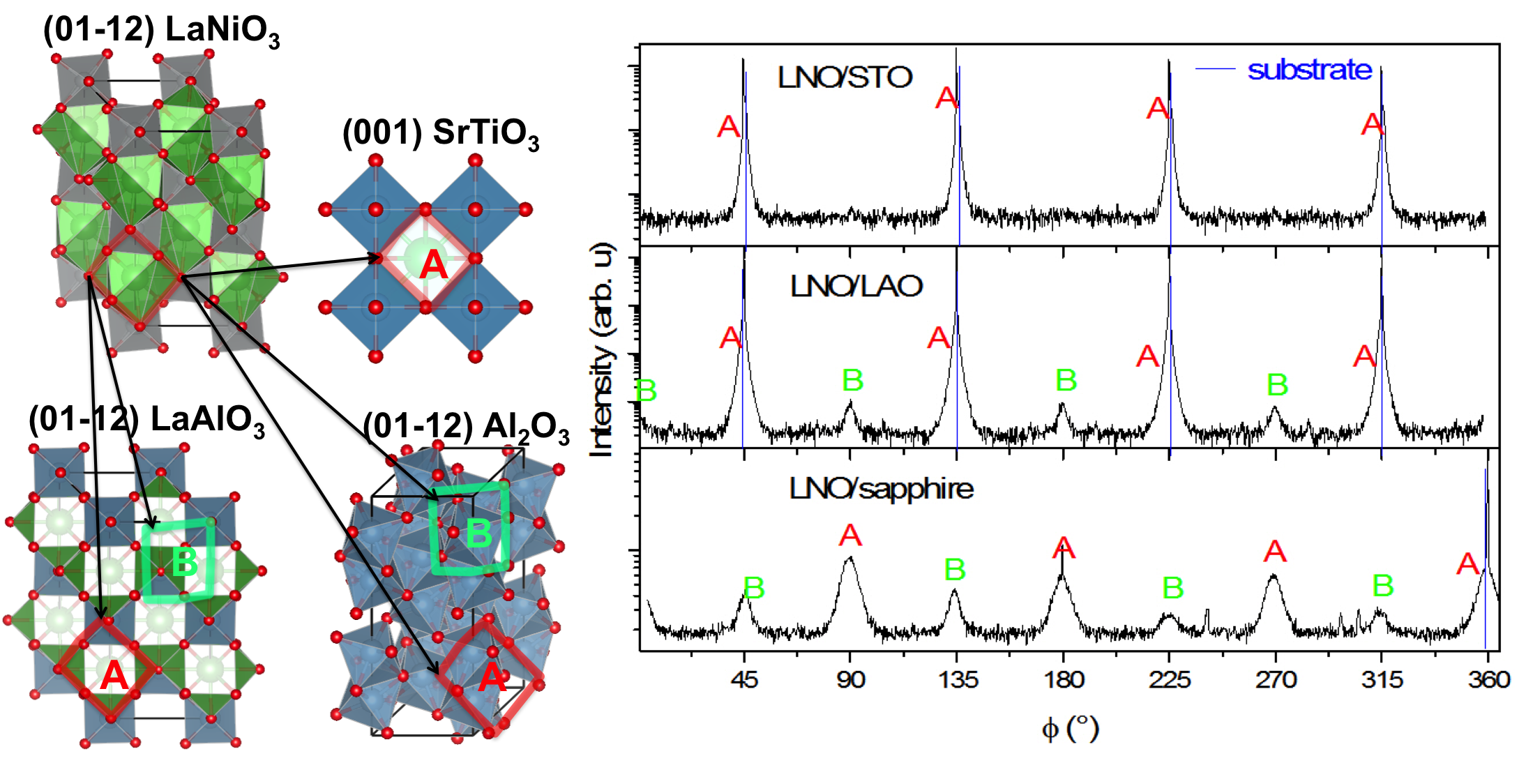
3.1.2. Evaporation Temperature

In the case of PIMOCVD and DLI-CVD, the influence of the evaporation temperature on the growth rate of the layer and the efficiency of evaporation of La and Ni precursors and their incorporation in the film was studied, which was represented by relationship, µ, between the La/Ni molar ratio in the grown film and the La/Ni molar ratio in the precursor solution (results are given in Figure 1a). The deposition temperature and pressure were set at 750 °C and 3.4 Torr in the DLI-CVD experiment and at 600 °C and 10 Torr in the PIMOCVD experiment, respectively.
According to the results obtained on the evaporation efficiency by DLI-CVD, the LNO growth rate and supplied La/Ni ratio were constant (165–170 nm/mmol) in the evaporation temperature range from 150 to 185 °C. Independently on the solvent used to dissolve the precursors, at evaporation temperatures higher than 185 °C, the growth rate started to decrease (by 1.3%/°C) while the µ ratio started to increase (by 1.5%/°C, up to µ = 0.64 at 215 °C) (Figure 1a). According to the thermogravimetric analysis of these precursors [21,31], the evaporation of Ni precursors are taken at lower temperatures than that of La(thd)3. 80% of solid precursor mass was evaporated at 220 and 270 °C at an atmospheric pressure, respectively. The liquid atomization technique and the vacuum conditions ameliorate the evaporation efficiency and decrease the evaporation temperature considerably. Thus, the temperatures of 150–185 °C are suitable for the evaporation of the Ni precursor but they are too low for the La precursor. Thus, the increase of the evaporator temperature up to 215 °C resulted in the increase of the La amount in the layer. This indicates, that the La–Ni system, in order to optimize the growth rate and to attain the fine control of the layer composition, would be preferable for using two separate evaporators and two separate tanks of solutions rather than a single evaporator with a single solution source. The corresponding decrease of the growth rate at temperatures below the precursor decomposition temperatures could be related to two origins: a density change of the layer or a difference of the growth rates of different La–Ni–O phases.
In the case of PIMOCVD, the maximum growth rate of 1135 nm/mmol and max µ = 0.66 was attained at an evaporation temperature of 250 °C, which indicates that optimal conditions for Ni evaporation can be attained at much higher temperatures in simple liquid injection systems as compared to DLI vapor supply systems. It is important to note that this difference in temperatures might be at least partially related to the difference in temperature homogeneity/thermocouple placement and efficiency of evaporator heating. A higher growth rate attained in the PIMOCVD reactor as compared to the DLI-CVD machine was related to a lower deposition temperature and a higher oxygen ratio in the precursor coordination sphere and in the solvent. The La amount in the layer increased with the growth of the evaporator temperature from 220 to 270 °C, which shows amelioration of its evaporation. It is important to note that, in the case of a single solution of La(thd)3 and Ni(thd)2 in 1,2-dimethoxyethane, a rearrangement/interaction between precursor and solvent molecules may appear to ameliorate La evaporation/incorporation. At evaporation temperatures higher than 270 °C, the La amount started to decrease, which indicates that the volume decomposition of the La precursor was accompanied with a further decrease of the growth rate (approximately 0.6%/°C).

3.1.3. Deposition Pressure and Injection Frequency

Figure 1b shows the impact of the operating pressure in PIMOCVD on the growth rate of the layer and the µ ratio. Other deposition parameters were kept constant: evaporation and substrate temperatures were set at 270 and 600 °C, respectively. As expected, increasing the pressure from 2.5–5 Torr drastically increased the growth rate (from 917 to 1450 nm/mmol) while µ remained around 0.71, which suggests that more precursors were involved in the formation of the layer as precursors stayed in the vicinity of the substrate for a longer period of time and/or more efficient evaporation. However, a further increase of the pressure up to 10–15 Torr resulted in diminishing the growth rate down to 750–800 nm/mmol and the µ ratio to 0.63. In the case of high pressures at high deposition temperatures, the flow rate of the precursors is low and the precursors can attain their decomposition temperature in the reactor volume and decompose before reaching the substrate. The decrease of the µ ratio by 0.08 suggests that La(thd)3 is less thermally stable and decomposes at a higher rate than Ni(thd)2.
In the case of PIMOCVD, the precursor injection frequency was varied from 1 to 2 Hz and no significant changes in the composition (La/Ni ratio in film 1.1 ± 0.2), resistivity (~9.7 × 10⁻⁴ ± 0.001 Ω cm), and roughness (~2.4 ± 0.1 nm) of deposited films were observed.

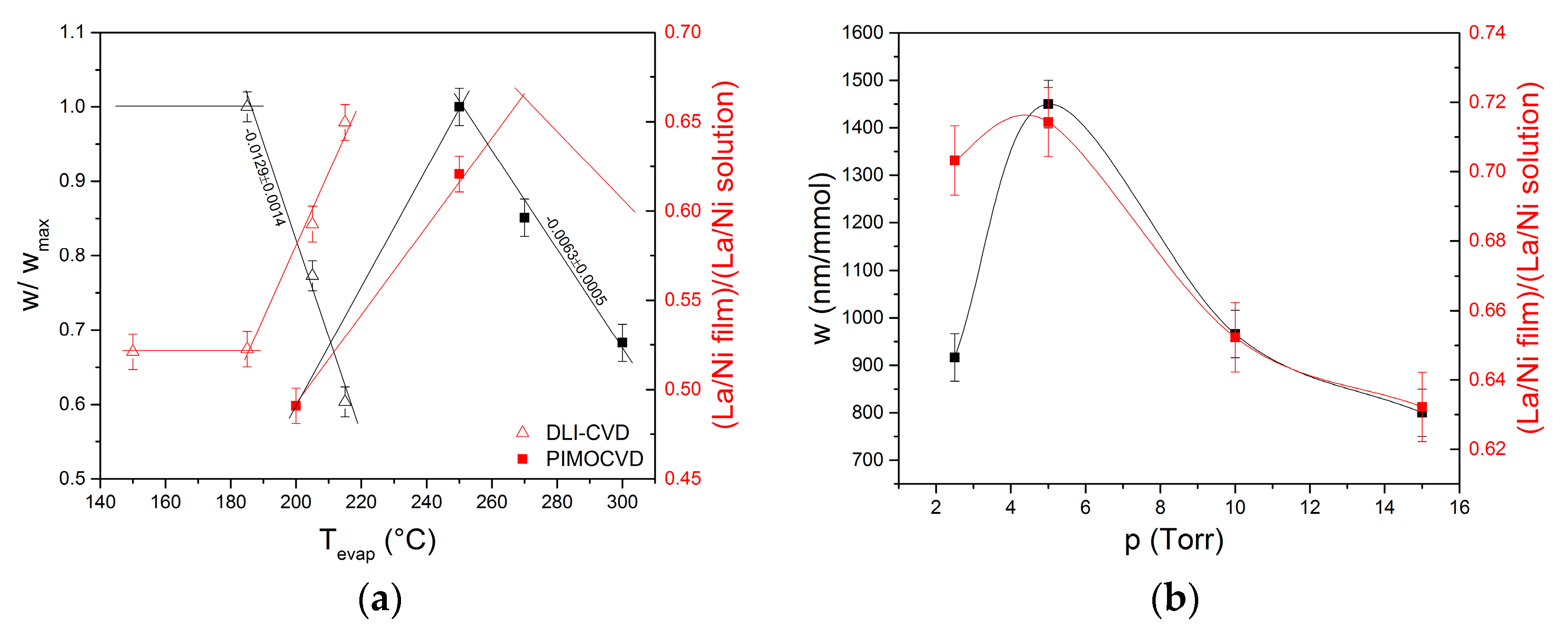
3.1.4. Deposition Temperature

The kinetics of APMOCVD and PIMOCVD processes, expressed as Arrhenius plots of the growth rate versus the deposition temperature, are represented in Figure 2. The evaporation temperature and pressure were set at 200 °C and 10 Torr in the PIMOCVD experiments, respectively. The 0.02 M solutions of La(thd)3 and Ni(thd)2 in monoglyme with La/Ni ratio in film of around 1.05 and 1.03 were used for PIMOCVD and APMOCVD depositions, respectively.
In the case of PIMOCVD, at temperatures below 500 °C, the growth rate was limited by chemical reaction kinetics and temperature (Regime I) and it increased linearly with an increasing deposition temperature based on the Arrhenius equation.
ln w = E a R T + ln A
where w is the growth rate (nm/min); A—pre-exponential factor, a constant for each chemical reaction (Arrhenius constant); Ea—activation energy; R—universal gas constant; and T—temperature. This regime was not observed in the case of APMOCVD, as the depositions at temperatures below 500 °C were not done. When the deposition temperature reached 500 °C, the growth rate remained constant with a further temperature rise to 575 and 600 °C in the case of APMOCVD and PIMOCVD, respectively. This indicates the diffusion or mass transport limited regime (Regime II) where the growth rate of the film mostly depends on the gas phase transport rate towards the nucleation surface. Maximum growth rates of 9.1 and 23.2 nm/min, as presented in Figure 2, were attained in this stage by PIMOCVD and APMOCVD, respectively. However, considering the amount of precursors used during the process, these maximum growth rates were 367 and 730 nm/mmol, respectively, which demonstrates a lower difference in the efficiency of two processes when the efficiency is expressed through the precursors yield. Increasing the growth temperature over 575 and 600 °C in APMOCVD and PIMOCVD, respectively, resulted in a decreasing growth rate due to the depletion of precursors (Regime III), which are related to the decomposition of precursors in the volume. In the case of DLI-CVD, no change in the growth rate was observed in the used deposition temperature range from 650 to 775 °C. Considerably higher temperature ranges of the Regime II in DLI-CVD as compared to PIMOCVD is related to the substrate heating method. In the DLI-CVD, the substrate holder has internal resistive heating to assure a high thermal gradient in the proximity of the substrate and to avoid the decomposition of precursors in the volume and thermalized reactor walls (at 250 °C) to avoid precursor condensation. In PIMOCVD, the hot wall reactor (external resistive furnace mounted on the quartz tube) was used. Thus, the temperature gradient was smaller in PIMOCVD than in DLI-CVD, which increases the probability of decomposition of precursors in the volume at high substrate temperatures. Moreover, the deposition took place on the reactor wall as well.

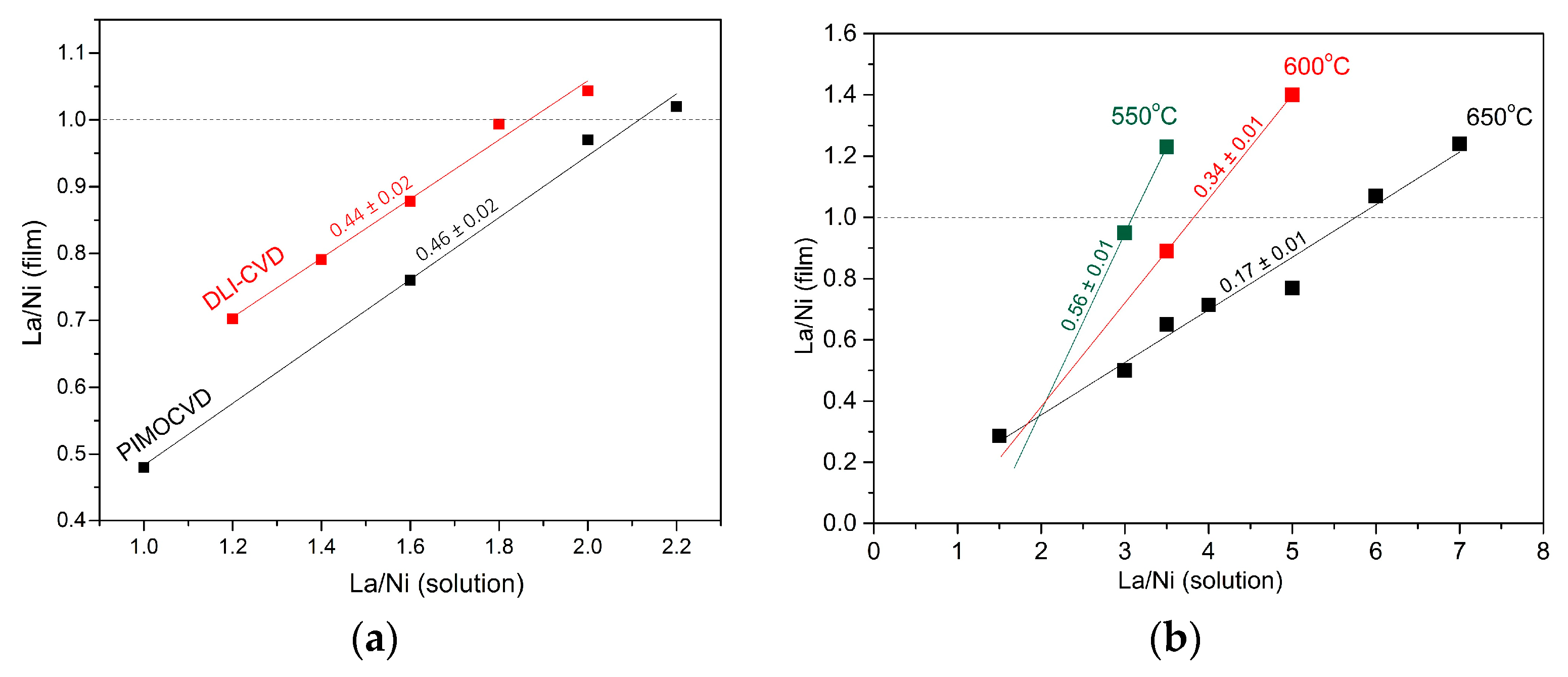
3.1.5. La/Ni Ratio in Solution

The relationship between La/Ni molar ratios in the film and in the solution of precursors were studied at deposition temperatures of 750 °C/700 °C and pressure of 3.4 Torr/10 Torr in DLI-CVD/PIMOCVD (Figure 3a), and at deposition temperatures of 550, 600, and 650 °C in APMOCVD (Figure 3b). It is important to note that temperatures >675 °C could not be used in APMOCVD for security reasons. The evaporation temperatures of 185 and 200 °C were used in DLI-CVD and PIMOCVD, respectively. In the case of all three methods, the La/Ni ratio in film depends linearly on the La/Ni ratio in the solution. However, the incorporation of La in films is really poor in the case of APMOCVD and it diminishes with the increase of the temperature (Figure 3b). To attain stoichiometric composition of LNO films (La/Ni = 1) deposited by means of APMOCVD, the La/Ni ratio in the solution had to be of 3.0, 3.8, and 5.8 at deposition temperatures of 550, 600, and 650 °C, respectively. It is important to note that the film growth by APMOCVD (Figure 2) was in a depletion regime at deposition temperatures of 600 and 650 °C. This indicated that the La precursor tends to decompose before reaching the substrate and it is less thermally stable than the Ni precursor. At high deposition temperatures during APMOCVD, the aerosol of the precursor solution evaporates before reaching the substrate and, in the depletion regime, the precursors start to decompose in the volume. In APMOCVD, the deposition atmosphere contains humidity and carbon dioxide, which easily react with La precursor derivatives and lanthanum oxide. This reduces drastically the efficiency of La2O3 incorporation in the growing layer. Therefore, considerably better efficiency in La incorporation in grown films was attained in vacuum deposition conditions (DLI-CVD and PIMOCVD). The stoichiometric LNO films were grown from solutions with La/Ni ratios of 1.8 and 2.1, respectively (Figure 3a). Although it seems that these specific DLI-CVD conditions were better adapted to the evaporation and/or deposition of La2O3 than PIMOCVD ones, the change of the film composition as a function the La/Ni ratio in the solution was represented by the same slope (0.45) in the case of both methods (Figure 3a). In the case of DLI-CVD and PIMOCVD, the µ ratio was independent of the deposition temperature in the range of 650–750 °C and 550–700 °C, respectively.

3.2. Properties of LaNiO3 Thin Films

The physical properties such as conductivity or resistivity are mainly defined by the film orientation, microstructural and lattice defects, and composition. The creation of some defects might be related to the deposition process itself such as the pinning of Ar+ ions in the films deposited by sputtering techniques [32]. Our films were deposited by the same type of deposition technique, CVD, and the difference in the precursor delivery systems will not actually alter the physical and structural properties of deposited films. The film quality will be mainly dependent on the deposition conditions (growth rate and deposition temperature) and the ability to optimize the deposition conditions and to control film composition [33,34]. Therefore, in this work, we intentionally do not compare the structural quality and resistivity of LNO films grown by three different CVD methods, and we prefer to focus on the microstructure and composition effects on the electrical properties.

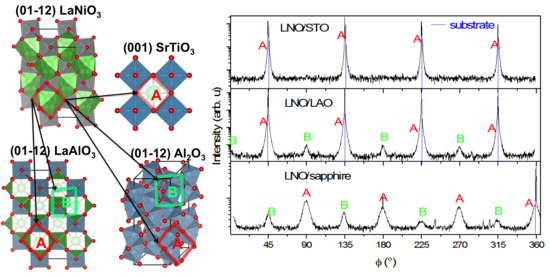
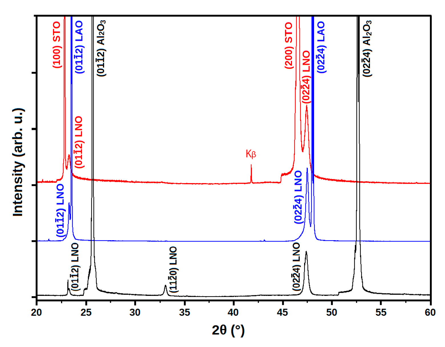
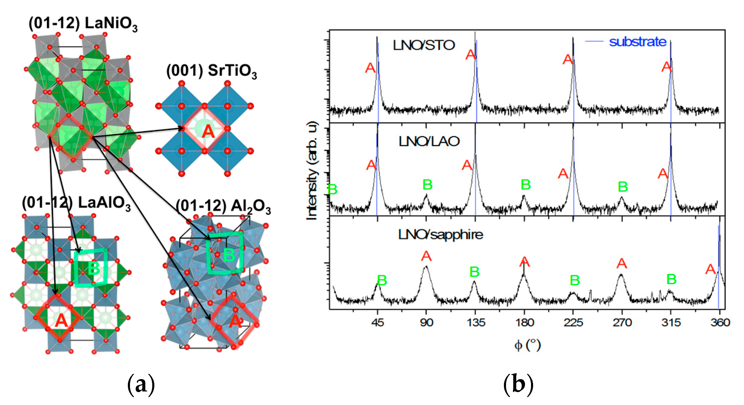
3.2.1. Structural Properties
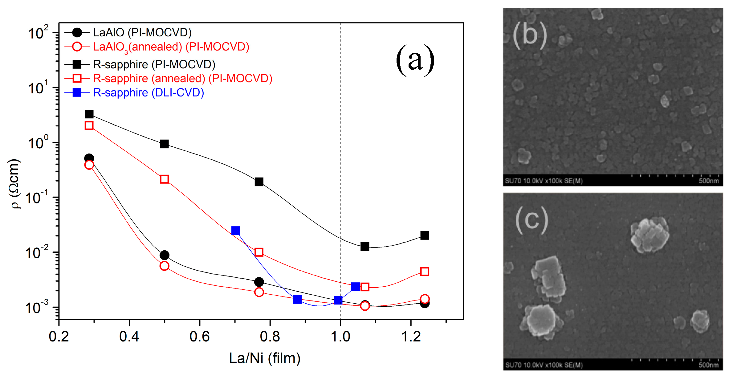
Texture and epitaxial quality of nearly stoichiometric LNO films grown with thickness of around 130 nm at 750 °C on R-sapphire substrates by DLI-CVD, and on (01 1 ¯ 2) LAO & (001) STO substrates by PIMOCVD were studied by means of XRD. According to θ/2θ patterns, LNO films on these three substrates presented <01 1 ¯ 2> planes parallel to the substrate surface (Figure 4). The films on LAO and STO substrates contained pure texture, while the films on R-sapphire presented volume fraction of 15% of (11 2 ¯ 0) oriented grains (volume fraction was estimated from the XRD reflection intensities normalized with respect to the theoretical intensities). The FWHM (full width at half maximum) of the rocking curve of (02 2 ¯ 4) reflections of LNO films on R-sapphire, LAO, and STO substrates were of 0.88°, 0.77°, and 0.63°, respectively (the instrumental resolution was of 0.23°). In order to determine the orientation of LNO films in the substrate plane, φ-scans of (0006) LNO reflection were measured (Figure 5). In a trigonal crystal structure, (0006) reflection of hexagonal cell is unique. Thus, a single reflection should be observed in φ-scans. However, three reflections of {20 2 ¯ 2} family planes present very close inter-planar distances and tilt the angle with respect to the (01 1 ¯ 2) planes to those of (0006) reflection (Figure 6). Therefore, the reflections of (0006) and {20 2 ¯ 2} planes of LNO and LAO cannot be separated in φ-scans and four reflections are observed. However, the intensity of {20 2 ¯ 2} LNO reflections is expected to be three times higher than that of (0006) LNO reflection. The φ-scans of LNO/STO films presented four reflections with equivalent intensities and with FWHM of 1.52° (Figure 5), which indicates a presence of four types of growth variants (hereafter named A-variants) rotated with respect to each other by 90° in the substrate plane. Similar A-variants were observed in the case of LNO films on LAO and sapphire substrates, as well. However, in the case of LNO/LAO and LNO/sapphire films, the second type of growth variants (B-variants), rotated by 45° in the substrate plane with respect to the A-variants was identified. There were four types of A-variants and B-variants rotated with respect to each other by 90° in the substrate plane and their volume fraction was similar in which four corresponding reflections presented similar intensities. The volume fractions of B-variants (estimated from intensities of corresponding reflections in φ-scans) were 1.3% and 23.6%, respectively. The FWHMs of (0006)/ {20 2 ¯ 2} reflections in φ-scans of A and B variants LNO/LAO (LNO/sapphire) films were 2.11° and 4.55° (7.0° and 5.8°), respectively.
The effect of deposition temperature on the texture and in-plane orientation of LNO films grown on LAO substrates by PIMOCVD was studied. The films grew epitaxial by forming A- and B-growth variants at deposition temperatures from 500 to 750 °C. The volume fraction of B-growth variants were 1.3%, 2.7% and 5.7% in the films grown at temperature of 750, 600, and 500 °C, respectively. The FWHM of the (024) rocking curves ((0006)/{20 2 ¯ 2} reflections in φ-scans of A variants) of LNO/LAO films grown at 750, 600, and 500 °C were 0.77° (2.11°), 1.11° (2.68°), and 1.09° (3.03°), respectively. The LNO/LAO films grown by APMOCVD at the temperature of 625 °C presented the mosaicity of 0.93°, the disorientation of A-variants in the substrate plane of 2.74°, and the volume fraction of B-variants of 16.6%. The LNO films on sapphire grown by APMOCVD at deposition temperature of 625 °C and by PIMOCVD at 500–650 °C did not present any preferential orientation in the substrate plane and any peak in the rocking curve measurements indicating very high mosaicity.

3.2.2. Resistivity

Resistivity of films, grown on LAO and sapphire substrates at 600 °C by PIMOCVD and on sapphire substrates at 750 °C by DLI-CVD, was characterized by a four-point probe technique at room temperature. The relationship between the La/Ni ratio in the film and the resistivity of films is presented in Figure 7. In the case of films grown by PIMOCVD, LNO/sapphire films showed resistivity of 1–2 orders higher than LNO/LAO layers. NiO-rich films had higher resistivity, and the resistivity was decreasing by increasing La2O3 amount in the layer towards nearly stoichiometric compositions. The lowest resistivities, attained in LNO/LAO and LNO/sapphire layers with nearly stoichiometric La/Ni ratio (around 1.05), were 1.09 × 10⁻³ and 1.26 × 10⁻² Ω cm, respectively. It is important to note that the resistivity of nearly stoichiometric LNO/LAO film was close to that of bulk LNO (ρbulk = 2.5 × 10⁻³ Ω cm) [2]. Further deviation from stoichiometric La/Ni ratio towards La2O3-rich compositions introduced an increase of resistivity, as well. The resistivities of LNO/LAO and LNO/sapphire layers grown at 500 °C by PIMOCVD were 2.16 × 10⁻³ and 1.06 Ω cm, respectively. The LNO/sapphire films, grown by DLI-CVD at 750 °C, presented similar change of resistivity as a function of La/Ni ratio in the film and showed the lowest resistivity values of 1.33 × 10⁻³–1.39 × 10⁻³ Ω cm at the La/Ni ratio of 0.88–1.0. The resistivity of LNO/sapphire films grown by DLI-CVD at temperature of 750 °C was lower by one order of magnitude as compared to those of PIMOCVD films deposited at 600 °C. The resistivities of films with La/Ni ratio close to 1.05, grown on LAO and sapphire substrates at 625 °C by APMOCVD were 3.60 × 10⁻³ and 7.20 × 10⁻³ Ω cm, respectively.
In order to study a role of defects in the conductivity and to ameliorate the crystallinity of LNO films grown by PIMOCVD at 600 °C, the studied LNO/LAO and LNO/sapphire films were annealed at 750 °C for 60 min in air. The resistivity of LNO/sapphire films reduced significantly (up to 81.5%). The decrease of resistivity was observed only in NiO-rich LNO/LAO films and it was markedly lower (3.7%) than in LNO/sapphire films. The minimum resistivities obtained in nearly stoichiometric LNO/LAO and LNO/sapphire films after annealing were 1.05 × 10⁻³ and 2.33 × 10⁻³ Ω cm, respectively. The LNO/sapphire films grown at 600 °C by PIMOCVD and annealed at 750 °C presented almost identical resistivity as the films grown directly at 750 °C by DLI-CVD.
SEM images of La2O3-poor (La/Ni = 0.9) and La2O3-rich (La/Ni = 1.02) LNO films are given in Figure 7b,c, respectively. Commonly, in the case of La2O3-rich films, the morphology of the films contained the hillocks, formed after deposition in ambient conditions (Figure 7c). This suggested that the surface of these films was reactive with humidity and/or CO2 present in the air. It is well known that lanthana is unstable in the air and forms hydroxides/carbonates [35,36]. These hillocks were not observed in stoichiometric and La2O3-poor films. The grain size was estimated by means of atomic force microscopy and the typical morphology of ( 01 1 ¯ 2 ) oriented films consisted of grains with the size of around 50 nm in the range of La/Ni ratio from 0.9 to 1.2.

4. Discussion

Ni(thd)2 presents very good volatility and stability at a temperature range of 150–250 °C and pressure of several Torr even though the volatility of Ni(thd)2 depends on the used solvent and the presence of water since it tends to coordinate oxygen containing solvents or Lewis bases. Thus, a particular attention should be given to the quality of used solvents and storage/preparation conditions. The major issues were encountered with La(thd)3 precursor since it presents lower volatility than Ni(thd)2. Although, its volatility can be increased with the increase of evaporation temperature without decomposition of Ni(thd)2, it starts to decompose at evaporation temperatures higher than 270 °C. This thermal instability of La(thd)3 precursor results in at least 40% lower efficiency of La2O3 integration to the layer as compared to NiO and in a strong dependence of the film composition on the deposition conditions such as deposition pressure, evaporation, and deposition temperatures. Therefore, lower pressure conditions are preferable especially at high deposition temperatures to generate a fast flow of precursors and to limit thermal exchanges of precursors with their environment even if the deposition efficiency might be reduced. This, in particular, applies to the hot-wall CVD reactors. In the case of hot-wall PIMOCVD, at a pressure of 5 Torr, the growth rate was constant in the temperature range from 500 to 600 °C. The depletion regime occurred above 600 °C, probably related to the precursor decomposition in the PIMOCVD reactor volume since the depletion regime was not observed in the temperature range of 650–775 °C in the DLI-CVD system with an internal substrate heating system. Thus, high thermal gradients should be used in order to avoid the volume decomposition of thermally instable precursors. The LNO films were successfully grown epitaxially on LAO substrates by PIMOCVD at deposition temperatures ≥500 °C and at relatively high deposition rates (9 nm/min) and the epitaxial quality of these films was slightly ameliorated by the increasing the deposition temperature. However, in the case of sapphire substrates, the epitaxial growth was not observed at these conditions. The films grown on sapphire by APMOCVD at deposition temperature of 625 °C were not epitaxial, as well. LNO was grown epitaxially on sapphire at 750 °C and at growth rate of 0.5 nm/min by means of DLI-CVD. Although, the regime limited by diffusion is usually used for the efficient growth of thin films by MOCVD, the temperatures ≥700 °C and low growth rates are needed to assure epitaxial growth on the substrates presenting the high lattice mismatch with the layer.
The texture and in-plane orientation quality is directly related to the matching of the film and the substrate lattices. As expected, LNO grew epitaxially on (100) cubic STO substrate, with epitaxial relationship of (110)STO‖(11 2 ¯ 0)LNO, (110)STO‖(01 1 ¯ 4)LNO, and (100)STO‖(01 1 ¯ 2)LNO, family planes with lattice mismatches of +1.3%, +2.6%, and +1.9%, respectively (Figure 6). The cubic symmetry of the surface plane of the STO substrate resulted in the four growth variants rotated with respect to each other by 90° in the substrate plane. LAO has a trigonal structure, but its (01 1 ¯ 2) orientation presents very small distortion and, in literature, this orientation of LAO is usually considered as a pseudo-cubic one. The four types of growth variants, rotated 90 ° with respect to each other in the substrate plane (A-type) were present in LNO/LAO films (Figure 5) with epitaxial relationships (lattice mismatch).
  • (11 2 ¯ 0)LAO‖(11 2 ¯ 0)LNO (−1.6%) and (01 1 ¯ 4)′LAO‖(01 1 ¯ 4)′LNO (−0.5%);
  • (11 2 ¯ 0)LAO‖( 1 ¯ 1 ¯ 20)LNO (−1.6%) and (01 1 ¯ 4)′LAO‖(0 1 ¯ 1 4 ¯ )′LNO (−0.5%);
  • (11 2 ¯ 0)LAO‖(01 1 ¯ 4)′LNO (−0.4%) and (01 1 ¯ 4)′LAO‖(11 2 ¯ 0)LNO (−1.8%);
  • (11 2 ¯ 0)LAO‖(0 1 ¯ 1 4 ¯ )′LNO (−0.4%) and (01 1 ¯ 4)′LAO‖( 1 ¯ 1 ¯ 20)LNO (−1.8%).
It is important to note that ( 01 1 ¯ 4 ) planes in a hexagonal cell of trigonal structure are tilted from the surface plane by a small angle (90°—χ, χ angles of ( 01 1 ¯ 4 ) planes of LNO, LAO, and sapphire can be found in Figure 6). In the case of LAO substrates, there was a second in-plane matching orientation-B variants. The ( 01 1 ¯ 4 ) and ( 1 ¯ 1 ¯ 20 ) family planes of B-variants were parallel to ( 01 1 ¯ 2 ) family planes of the LAO substrate and ( 01 1 ¯ 2 ) LNO planes parallel to ( 01 1 ¯ 4 ) LAO and ( 1 ¯ 1 ¯ 20 ) LAO planes. To match the LAO lattice, three interplanar (01 1 ¯ 4)′LNO distances, d LNO ( 01 1 ¯ 4 ) , of B-variants fit on two d LAO ( 01 1 ¯ 2 ) (with lattice mismatch of 6.1%), 3 × d LNO ( 11 2 ¯ 0 ) 2 × d LAO ( 01 1 ¯ 2 ) (6.1%), 2 × d LNO ( 01 1 ¯ 2 ) 3 × d LAO ( 11 2 ¯ 0 ) (5.0%), and 2 × d LNO ( 01 1 ¯ 2 ) 3 × d LAO ( 01 1 ¯ 4 ) (4.9%). The worse lattice matching of B-variants requiring plane arrangement in a longer range on the LAO substrate resulted in their small volume fraction and worse quality of in-plane orientation as compared to A-variants. The long-range order is ameliorated at higher deposition temperatures due to increased surface mobility of atoms. Therefore, the volume fraction of B-variants in LNO/LAO films was decreased from 5.7% to 1.3% by increasing the deposition temperature from 500 to 750 °C. The mobility of atoms is highly limited at atmospheric pressure and at high deposition rates, used for APMOCVD, thus, the volume fraction of B-variants was considerably higher (16.6%) comparing to that in PIMOCVD films grown at similar temperature (2.7%).
In the case of trigonal ( 01 1 ¯ 2 ) sapphire substrates, eight (0006)/(20 2 ¯ 2) reflections were observed in φ-scans, which indicates a presence of A-variants and B-variants with equivalent lattice arrangements to those on LAO substrate. The lattice mismatch of A-variants with sapphire lattice was of −12.7% for ( 11 2 ¯ 0 ) sapph ( 11 2 ¯ 0 ) LNO , −5.2% for ( 01 1 ¯ 4 ) sapph ( 01 1 ¯ 4 ) LNO , and +9.2% for ( 01 1 ¯ 2 ) sapph ( 01 1 ¯ 2 ) LNO planes. In the case of B-variants, the mismatch of −13.8% is present for 3 × d LNO ( 01 1 ¯ 4 ) 2 × d sapph ( 01 1 ¯ 2 ) , −14.9% for 3 × d LNO ( 11 2 ¯ 0 ) 2 × d sapph ( 01 1 ¯ 2 ) , −6.8% for 2 × d LNO ( 01 1 ¯ 2 ) 3 × d sapph ( 11 2 ¯ 0 ) , and −0.1% for 2 × d LNO ( 01 1 ¯ 2 ) 3 × d sapph ( 01 1 ¯ 4 ) . The volume fraction of B-variants was much higher in LNO/sapphire films (23.6%) than in LNO/LAO films (1.3%). The lattice mismatches were considerable for both types of variants in LNO/sapphire layers. However, the formation of A-variants was favored by the alignment of the dense ( 01 1 ¯ 2 ) planes and the reproduction of the surface symmetry of the sapphire substrate. To summarize, the interplanar distances of perpendicular planes to the ( 01 1 ¯ 2 ) plane of LNO are matching well in-plane parameters of (100) STO and ( 01 1 ¯ 2 ) LAO substrates (with higher mismatch in the case of LAO substrates). The surface of the R-sapphire surface is less compatible with an LNO structure. This is directly reflected in the texture and in-plane orientation quality. The highest epitaxial quality of LNO films was obtained on STO and LAO substrates.
Although, in cubic/tetragonal/orthorhombic materials only lattice parameters are considered in the epitaxial relationships. It is important to note that, in trigonal materials, the angle between ( 11 2 ¯ 0 ) planes and ( 01 1 ¯ 2 ) planes (see angle φ in Figure 7) is not equal to 45° as in cubic materials. In the case of sapphire substrate, this deviation from 45° is of 2.14° while it is only of 0.36° (0.04°) in LNO (LAO). Therefore, to match the sapphire substrate, LNO unit cells had to rotate by several degrees in the sapphire substrate plane introducing considerable dispersion of the in-plane orientation (represented by high FWHM of reflections in φ-scans), while, in the case of LAO and STO substrates, LNO had incompatibility in ( 01 1 ¯ 2 ) plane alignment of 0.32°–0.36° and the quality of in-plane orientation was better.
Since LNO films on sapphire and LAO substrates had the same growth orientation and were grown at the same deposition conditions (oxygen concentration should be the same in both films), the difference in resistivity of these films can be explained only by microstructural defects. The LNO/sapphire films presented higher B-variant concentration, a lower quality of texture and in-plane orientation, and, consequently, a higher density of defects and grain boundaries than LNO/LAO films. The LNO/LAO films grown by PIMOCVD at 500–600 °C and by APMOCVD at 625 °C presented similar quality of texture and in-plane orientation but they had different B-variant fraction. The films with higher B-variant volume fraction (2.7%, –5.7%, −16.6%) showed higher resistivity (1.09 × 10⁻³, −2.16 × 10⁻³, −3.60 × 10⁻³ Ω cm). This indicates that grain boundaries play an important role in the resistivity of LNO films and tend to increase it. It is expected that annealing in oxygen atmosphere at high temperatures would compensate the oxygen vacancies present after deposition and would reduce the resistivity of the LNO films [37]. It is important to note, that annealing at higher temperatures than those used for the deposition results in a recrystallization of films and decrease of the crystalline defects, as well. The resistivity of LNO/sapphire films after annealing at 750 °C decreased significantly while the resistivity of nearly stoichiometric LNO/LAO film remained almost the same. It is important to note, that the epitaxial quality of LNO/LAO films was little changing with the increased deposition temperature from 600 to 750 °C thus, little amelioration of crystalline quality is expected in the LNO/LAO films during thermal treatment at 750 °C. The LNO/sapphire films were not epitaxial and significant lattice rearrangement took place resulting in the decrease of resistivity during annealing and the resistivities close to those of the films grown directly at 750 °C with low deposition rates were attained. This also indicates that the oxygen deficiency does not seem to be the main origin of increased resistivity in LNO films grown by CVD, as the films were grown at a relatively low vacuum and the partial pressure of oxygen was around 40%. To summarize, the oxygen vacancies could contribute at least partially to the decrease of the resistivity of LNO films grown by CVD at pressures of several Torr and with a partial oxygen pressure of 40%. However, the main origin of increased resistivity in LNO films can be attributed to the deviation from nearly stoichiometric La/Ni ratio or to the increased microstructural defects such as grain boundaries. In the case of epitaxial films, the grain boundary density is mainly related to the volume fraction of the growth variants.

5. Conclusions

The solvents such as monoglyme and TMEDA, able to act as a Lewis basis, coordinated to the Ni(thd)2 precursor and ameliorated its volatility and solubility in mesitylene and toluene. The major encountered issues were related to the high evaporation temperature and thermal instability of La(thd)3, which introduced the necessity to use the excess of the La precursor in the solution and the dependence of film composition on deposition parameters such as pressure and deposition temperature. The best epitaxial quality of (01 1 ¯ 2) LNO films was obtained on (100) STO and (01 1 ¯ 2) LAO substrates. Although, epitaxial growth of this LNO orientation was also attained on R-sapphire substrates, the rhombohedral distortion of R-sapphire was too big to match properly angular relationships between LNO crystallographic planes, which resulted in considerable mosaicity and dispersion of in-plane orientation. “Cube on cube” growth was dominant in the case of all three substrates. However, the second type of growth variants, rotated by 45° in the substrate plane with respect to the matrix of the film, appeared in the LNO films grown on LAO and sapphire. The resistivity of LNO films, grown by CVD, was mainly defined by composition deviation from stoichiometry and by microstructural defects. The annealing in oxygen atmosphere of high epitaxial quality LNO/LAO films with nearly stoichiometric La/Ni ratio had little effect on the resistivity, which suggests a minor presence of oxygen vacancies in as-grown films. The increased volume fraction of growth variants resulted in the increased grain boundary density and consequently in the increased resistivity. The similar annealing of LNO films on sapphire considerably reduced the resistivity likely due to the reduction of microstructural defects.

Author Contributions

Conceptualization, A.B.; Methodology, J.-M.D., A.A., V.P., C.M., and A.B.; Validation, S.K., and V.A.; Formal Analysis, S.K., V.A., and A.B.; Investigation, S.K., V.A., A.A., V.P., P.B., and A.B.; Resources, Z.S., C.M., P.B., and S.M.; Data Curation, S.K., V.A., P.B., and S.M.; Writing–Original Draft Preparation, S.K., V.A., and A.B.; Writing–Review & Editing, A.B., J.-M.D., V.P., S.K., V.A., and A.A.; Supervision, A.B., C.M., A.A., and V.P.; Project Administration, A.B.; Funding Acquisition, A.B. and J.-M.D.

Funding

This research was funded by the French RENATECH network, SME Annealsys, Bourgogne Franche-Comté region, EUR EIPHI program (ANR-17-EURE-0002) and French National Research Agency funding ANR LiLit (ANR-16-CE24-0022-011).

Acknowledgments

Authors would like to thank Virgaudas Kubilius for the development of the four-probe measurement of resistivity at Vilnius University.

Conflicts of Interest

The authors declare no conflict of interest. The funders had no role in the design of the study, in the collection, analyses, or interpretation of data, in the writing of the manuscript, or in the decision to publish the results.

References

  1. Ramesh, R.; Gilchrist, H.; Sands, T.; Keramidas, V.G.; Haakenaasen, R.; Fork, D.K. Ferroelectric La–Sr–Co–O/Pb–Zr–Ti–O/La–Sr–Co–O heterostructures on silicon via template growth. Appl. Phys. Lett. 1993, 63, 3592–3594. [Google Scholar] [CrossRef]
  2. Satyalakshmi, K.M.; Mallya, R.M.; Ramanathan, K.V.; Wu, X.D.; Brainard, B.; Gautier, D.C.; Vasanthacharya, N.Y.; Hegde, M.S. Epitaxial metallic LaNiO3 thin films grown by pulsed laser deposition. Appl. Phys. Lett. 1993, 62, 1233–1235. [Google Scholar] [CrossRef]
  3. Aytug, T.; Kang, B.W.; Cantoni, C.; Specht, E.D.; Paranthaman, M.; Goyal, A.; Christen, D.K.; Verebelyi, D.T.; Wu, J.Z.; Ericson, R.E.; et al. Growth and characterization of conductive SrRuO3 and LaNiO3 multilayers on textured Ni tapes for high-Jc YBa2Cu3O7−δ coated conductors. J. Mater. Res. 2001, 16, 2661–2669. [Google Scholar] [CrossRef]
  4. Garcia-Munoz, J.L.; Rodriguez-Carvajal, J.; Lacorre, P.; Torrance, J.B. Neutron-diffraction study of RNiO3 (R = La, Pr, Nd, Sm): Electronically induced structural changes across the metal-insulator transition. Phys. Rev. B Condens. Matter. 1992, 46, 4414–4425. [Google Scholar] [CrossRef] [PubMed]
  5. Meng, X.; Sun, J.; Yu, J.; Wang, G.; Guo, S.; Chu, J. Enhanced fatigue property of PZT thin films using LaNiO3 thin layer as bottom electrode. Appl. Phys. A 2001, 73, 323–325. [Google Scholar] [CrossRef]
  6. Guerrero, C.; Sanchez, F.; Ferrater, C.; Roldán, J.; García-Cuenca, M.V.; Varela, M. Pulsed laser deposition of epitaxial PbZrxTi1−xO3 ferroelectric capacitors with LaNiO3 and SrRuO3 electrodes. Appl. Surf. Sci. 2000, 168, 219–222. [Google Scholar] [CrossRef]
  7. Benckiser, E.; Haverkort, M.W.; Brück, S.; Goering, E.; Macke, S.; Frañó, A.; Yang, X.; Andersen, O.K.; Cristiani, G.; Habermeier, H.-U.; et al. Orbital reflectometry of oxide heterostructures. Nat. Mater. 2011, 10, 189–193. [Google Scholar] [CrossRef] [Green Version]
  8. Jang, A.N.; Seung, S.K.; Choi, K.H.; Song, J.H. Epitaxial growth and electrical transport property of artificial LaNiO3/LaAlO3 superlattices. Ceram. Int. 2012, 38, S627–S630. [Google Scholar] [CrossRef]
  9. Guo, X.; Li, C.; Zhou, Y.; Chen, Z. High-quality LaNiO3 thin-film electrode grown by pulsed laser deposition. J. Vac. Sci. Technol. A 1999, 17, 917–920. [Google Scholar] [CrossRef]
  10. Kim, S.S.; Kang, T.S.; Je, J.H. Microstructures of LaNiO3 films grown on Si(001) by pulsed laser deposition. Thin Solid Films 2002, 405, 117–121. [Google Scholar] [CrossRef]
  11. Li, A.; Ge, C.; Lü, P.; Ming, N. Preparation of perovskite conductive LaNiO3 films by metalorganic decomposition. Appl. Phys. Lett. 1996, 68, 1347–1349. [Google Scholar] [CrossRef]
  12. Wakiya, N.; Azuma, T.; Shinozaki, K.; Mizutani, N. Low-temperature epitaxial growth of conductive LaNiO3 thin films by RF magnetron sputtering. Thin Solid Films 2002, 410, 114–120. [Google Scholar] [CrossRef]
  13. Lane, P.A.; Crosbie, M.J.; Wright, P.J.; Donohue, P.P.; Hirst, P.J.; Reeves, C.L.; Anthony, C.J.; Jones, J.C.; Todd, M.A.; Williams, D.J. The metal–organic chemical vapor deposition of lanthanum nickelate electrodes for use in ferroelectric devices. Chem. Vapor Depos. 2003, 9, 87–92. [Google Scholar] [CrossRef]
  14. Korsakov, I.; Mankevich, A.; Tsymbarenko, D.; Makarevich, A.M.; Murzina, T.; Kaul, A. Epitaxial heterostructures of KNbO3/LaNiO3/SrTiO3 and KNbO3/La1−xKxMnO3/SrTiO3: MOCVD preparation and properties. ECS Trans. 2009, 25, 513–519. [Google Scholar]
  15. Seim, H.; Mölsä, H.; Nieminen, M.; Fjellvåg, H.; Niinistö, L. Deposition of LaNiO3 thin films in an atomic layer epitaxy reactor. J. Mater. Chem. 1997, 7, 449–454. [Google Scholar] [CrossRef]
  16. Qiao, L.; Bi, X. Direct observation of Ni3+ and Ni2+ in correlated LaNiO3−δ films. Europhys. Lett. 2011, 93, 57002. [Google Scholar] [CrossRef]
  17. Kuzmina, N.; Malkerova, I.; Ryazanov, M.; Alikhanyan, A.; Rogachev, A.; Gleizes, A.N. Volatility studies on single source precursors for LaNiO3 film deposition: Mass spectrometry and thermal analysis. J. Phys. IV France 2001, 11, 661–667. [Google Scholar] [CrossRef]
  18. Hassan, A.J. Study of optical and electrical properties of nickel oxide (NiO) thin films deposited by using a spray pyrolysis technique. J. Mod. Phys. 2014, 5, 2184–2191. [Google Scholar] [CrossRef]
  19. Gorbenko, O.Y.; Bosak, A.A. Growth of LaNiO3 thin films on MgO by flash MOCVD. J. Cryst. Growth 1998, 186, 181–188. [Google Scholar] [CrossRef]
  20. Abrutis, A.; Bartasyte, A.; Garcia, G.; Teiserskis, A.; Kubilius, V.; Saltyte, Z.; Faucheux, V.; Figueras, A.; Rushworth, S. Metal-organic chemical vapour deposition of mixed-conducting perovskite oxide layers on monocrystalline and porous ceramic substrates. Thin Solid Films 2004, 449, 94–99. [Google Scholar] [CrossRef]
  21. Eisentraut, K.J.; Sievers, R.E. Thermogravimetric studies of metal β-diketonates. J. Inorg. Nucl. Chem. 1967, 29, 1931–1936. [Google Scholar] [CrossRef]
  22. Burriel López, M. Epitaxial Thin Films of Lanthanum Nickel Oxides: Deposition by PI-MOCVD, Structural Characterization and High Temperature Transport Properties. Ph.D. Thesis, Universitat Autònoma de Barcelona, Bellaterra, Spain, March 2007. [Google Scholar]
  23. Bartasyte, A.; Bouregba, R.; Dogheche, E.; Boudard, M.; Poullain, G.; Chaix-Pluchery, O.; Jimenez, C.; Plausinaitiene, V.; Remiens, D.; Abrutis, A.; et al. Ferroelectric PbTiO3 films grown by pulsed liquid injection MOCVD. Surf. Coat. Technol. 2007, 201, 9340–9344. [Google Scholar] [CrossRef]
  24. Bartasyte, A.; Abrutis, A.; Jimenez, C.; Weiss, F.; Chaix-Pluchery, O.; Saltyte, Z. Ferroelectric PbTiO3 films grown by pulsed liquid injection metalorganic chemical vapour deposition. Ferroelectrics 2007, 353, 104–115. [Google Scholar] [CrossRef]
  25. Kuprenaite, S.; Murauskas, T.; Abrutis, A.; Kubilius, V.; Saltyte, Z.; Plausinaitiene, V. Properties of In-, Ga-, and Al-doped ZnO films grown by aerosol-assisted MOCVD: Influence of deposition temperature, doping level and annealing. Surf. Coat. Technol. 2015, 271, 156–164. [Google Scholar] [CrossRef]
  26. Cabello, M.; Varghese, A.; Montserrat, J.; Rebollo, J.; Decams, J.M.; Godignon, P. Analysis of ZrxSiyOz as High-k Dielectric for 4H-SiC MOSFETs. Mater. Sci. Forum 2018, 924, 939–942. [Google Scholar] [CrossRef]
  27. What does DLI mean? Available online: https://www.annealsys.com/applications/dli-processes/what-does-dli-mean-ty20804.html (accessed on 20 September 2018).
  28. Bartasyte, A.; Plausinaitiene, V.; Abrutis, A.; Stanionyte, S.; Margueron, S.; Kubilius, V.; Boulet, P.; Huband, S.; Thomas, P.A. Thickness dependent stresses and thermal expansion of epitaxial LiNbO3 thin films on C-sapphire. Mater. Chem. Phys. 2015, 149–150, 622–631. [Google Scholar] [CrossRef]
  29. Astié, V.; Millon, C.; Decams, J.-M.; Bartasyte, A. Direct liquid injection chemical vapor deposition. In Chemical Vapor Deposition for Nanotechnology; Pietro, M., Ed.; InTech: Vienna, Austria, 2018. [Google Scholar]
  30. Soukup, R.W.; Schmid, R. Metal complexes as color indicators for solvent parameters. J. Chem. Educ. 1985, 62, 459. [Google Scholar] [CrossRef]
  31. Jones, A.C. MOCVD of electroceramic oxides: A precursor manufacturer’s perspective. In Proceedings of the Twelfth European Conference on Chemical Vapour Deposition, Sitges, Spain, 10–15 September 1999; pp. 169–179. [Google Scholar]
  32. Kuprenaite, S.; Margueron, S.; Raschetti, M.; Millon, C.; Baron, T.; Daniau, W.; Ballandras, S.; Gautier, B.; Albertini, D.; Boulet, P.; et al. Effect of LiNbO3 polarity on the structural, optical and acoustic properties of epitaxial ZnO and MgxZn1−xO films. J. Phys. D Appl. Phys. 2018, 51, 484003. [Google Scholar] [CrossRef]
  33. Margueron, S.; Bartasyte, A.; Plausinaitiene, V.; Abrutis, A.; Boulet, P.; Kubilius, V.; Saltyte, Z. Effect of deposition conditions on the stoichiometry and structural properties of LiNbO3 thin films deposited by MOCVD. In Oxide-based Materials and Devices IV, Proceedings of SPIE OPTO, San Francisco, CA, USA, 2–7 February 2013; Teherani, F.H., Look, D.C., Rogers, D.J., Eds.; SPIE: Bellingham, WA, USA, 2013. [Google Scholar]
  34. Bartasyte, A.; Margueron, S.; Baron, T.; Oliveri, S.; Boulet, P. Toward high-quality epitaxial LiNbO3 and LiTaO3 thin films for acoustic and optical applications. Adv. Mater. Interfaces 2017, 4, 1600998. [Google Scholar] [CrossRef]
  35. Bernal, S.J.A.D.; Diaz, J.A.; Garcia, R.; Rodriguez-Izquierdo, J.M. Study of some aspects of the reactivity of La2O3 with CO2 and H2O. J. Mater. Sci. 1985, 20, 537–541. [Google Scholar] [CrossRef]
  36. Zhao, Y. Design of higher-k and more stable rare earth oxides as gate dielectrics for advanced CMOS devices. Materials 2012, 5, 1413–1438. [Google Scholar] [CrossRef]
  37. Qiao, L.; Bi, X. Direct observation of oxygen vacancy and its effect on the microstructure, electronic and transport properties of sputtered LaNiO3−δ films on Si substrates. Thin Solid Films 2010, 519, 943–946. [Google Scholar] [CrossRef]
Figure 1. Growth rate (nm/mmol) and relationship between La/Ni molar ratios in the film and in the solution of precursors as a function of (a) evaporation temperature, used in DLI-CVD and PIMOCVD (the growth rate was normalized with respect to the maximum growth rate attained by that method; the maximum growth rates were 1135 and 169 nm/mmol in PIMOCVD and DLI-CVD processes, respectively). (b) Pressure during the PIMOCVD process.
Coatings 09 00035 g001
Figure 2. Arrhenius relationship between the growth rate of LNO films and the deposition temperature during APMOCVD and PIMOCVD processes. Regime I is a kinetic regime. Regime II is a diffusion or mass transport regime and Regime III is a depletion regime.
Coatings 09 00035 g002
Figure 3. Relationship between La/Ni molar ratios in the LNO film and in the solution of precursors: (a) at deposition temperatures of 750 and 700 °C in DLI-CVD and PIMOCVD, respectively; (b) at deposition temperatures of 550, 600, and 650 °C in APMOCVD.
Coatings 09 00035 g003
Figure 4. θ/2θ XRD patterns of LNO films with thickness of around 130 nm grown at 750 °C on R-sapphire substrates by DLI-CVD, and on (01 1 ¯ 2 ) LAO & (001) STO substrates by PIMOCVD. Note that the narrow reflections without labels correspond to the Kβ reflections of the substrates.
Coatings 09 00035 g004
Figure 5. (a) Projections of polyhedral structure representations along the normal to the plane (001) of SrTiO3 and to the (01 1 ¯ 2) planes of LaNiO3, LaAlO3, and Al2O3. Red balls represent oxygen anions, green balls–lanthanum or strontium cations, and blue balls–nickel, titanium, or aluminum cations. The LaNiO3 cell matching on the surface of SrTiO3, LaAlO3, and Al2O3 are illustrated as well. The growth variants, rotated in the substrate plane by 45° with respect to each other, were named A and B. (b) XRD φ-scans of (0006)/{20 2 ¯ 2} planes of LaNiO3 films on SrTiO3, LaAlO3, and Al2O3 substrates.
Coatings 09 00035 g005
Figure 6. Stereographic projections along the normal to the (100) planes of cubic SrTiO3 and to the (01 1 ¯ 2) planes of hexagonal cell of trigonal LaAlO3, LaNiO3, and Al2O3. Comparison of interplanar distances, d, and tilt angles, χ, in-plane rotation, φ, of major planes of cubic and hexagonal cells.
Coatings 09 00035 g006
Figure 7. (a) Composition dependence of resistivity of as-deposited and annealed (at 750 °C) LaNiO3 films on LaAlO3 and R-sapphire substrates grown by PI-MOCVD at 600 °C and by DLI-CVD at 750 °C. The resistivity SEM image of LaNiO3 film morphology with (b) La2O3-poor (La/Ni = 0.9) and (c) La2O3-rich (La/Ni = 1.02) compositions.
Coatings 09 00035 g007
Table 1. Substrates and deposition conditions used for the growth of LNO films by PIMOCVD, APMOCVD, and DLI-CVD.
Deposition ParametersPIMOCVDAPMOCVDDLI-CVD
SubstratesLaAlO3, R-Sapphire, SrTiO3, SiLaAlO3, R-Sapphire, SiR-Sapphire
Deposition temperature (°C)450–750500–675650–750
Evaporation temperature (°C)200–300150–215
Carrier gasAr + O2N2 + O2Ar + N2 + O2
Total pressure (Torr)5–157603.4
Partial O2 pressure (%)201040
Solution concentration (mol/L)0.020.020.01
Film thickness (nm)120–300120–26060–140

