Abstract
This work compares the deposition of aluminum nitride by magnetron sputtering on silicon to multilayer ceramic substrates. The variation of sputter parameters in a wide range following a fractional factorial experimental design generates diverse crystallographic properties of the layers. Crystal growth, composition, and stress are distinguished because of substrate morphology and thermal conditions. The best c-axis orientation of aluminum nitride emerges on ceramic substrates at a heater temperature of 150 °C and sputter power of 400 W. Layers deposited on ceramic show stronger c-axis texture than those deposited on silicon due to higher surface temperature. The nucleation differs significantly dependent on the substrate. It is demonstrated that a ceramic substrate material with an adapted coefficient of thermal expansion to aluminum nitride allows reducing the layer stress considerably, independent on process temperature. Layers sputtered on silicon partly peeled off, while they adhere well on ceramic without crack formation. Direct deposition on ceramic enables thus the development of optimized layers, avoiding restrictions by stress compensating needs affecting functional properties.
1. Introduction
Sputtered aluminum nitride (AlN), depending on composition and microstructure, can fulfill several functional demands such as optical functionalization [1,2], high-k dielectric [3,4], piezoelectric element [5,6], microelectromechanical systems (MEMS) resonators [6] or heat spreader [7]. It is therefore widely used in electronic circuits and MEMS devices. To employ the pyro- and piezoelectric properties in microelectromechanical and electronic devices, c-axis oriented AlN is required [8,9]. The same holds also for acousto-electronic devices [10,11], nonlinear optics and optomechanical devices, [12] as well as phononic crystals [13].
Usually, silicon is the substrate of choice for the device processing. Since the coefficient of thermal expansion (CTE) of silicon and AlN differs, thermal mismatch causes significant residual stress dependent on process temperature [14]. Strategies exist, such as variation of the N2/Ar ratio during the process [15], which compensate thermal stress by intrinsic stress components. However, this method entails an increase of lattice failures and thus, limitations of desired functional properties must be accepted. The use of substrates with adapted CTE would eliminate these disadvantages.
Low temperature co-fired ceramic (LTCC) stands for a technology, which uses green ceramic foils consisting of ceramic and glass powder, embedded in an organic matrix, for the fabrication of multilayer circuit boards with printed electronic components [16,17]. High reliability and temperature stability completed by a wide freedom in design and the possible integration of low resistivity conductor paths made of gold or silver boosts their application as radio frequency (RF) devices [18,19,20,21] and for smart system integration [22,23,24]. The composite character of the fired ceramic allows the variation of functional properties, such as permittivity, thermal expansion, or insulation resistance [25,26]. This flexibility, which entails the possibility of using a substrate with adapted CTE, was the first motivation for this study.
A second motivation originates from packaging aspects: Multiple device chips and passives are assembled on package carriers. Connections between chips, carrier, and passives require space and reduce the performance due to parasitic losses. The monolithic integration of functional units on the package contributes to cost reduction and system miniaturization. It requires the direct deposition of functional thin film components on LTCC ceramics [27].
Sputtering of AlN on LTCC substrates with high c-axis orientation would open new integration aspects. First works on this topic focused on the application of AlN as a heat spreader [7,28]. The used LTCC ceramic in this study has still a CTE mismatch and the layer was sputtered on the pristine and therefore rough ceramic surface. The roughness influences the grain structure and c-axis orientation is disturbed.
In the present study, a CTE adapted LTCC ceramic is used and the surface is polished in order to achieve the best conditions for textured layer growth. Morphological properties and layer stress of AlN layers sputtered on (100) silicon and LTCC ceramic are compared. The setup of the sputter coater supports high deposition rates, which allows the deposition of reasonable film thickness in acceptable process time. The experimental design covers a wide parameter range in order to assess a wide process window. The current investigation is a first step towards the deposition of well-textured AlN layers on polished LTCC surfaces with minimized stress. The parallel coating of ceramic and silicon substrates provides an insight into the growth process depending on the substrate.
2. Experimental Procedure
2.1. Sample Preparation
The CTE of sputtered AlN layers with (002) texture amounts to 5.3 × 10⁻⁶ K−1 along the c-axis and 4.2 × 10⁻⁶ K−1 in the basal plane according to the literature [29]. A commercially available LTCC green foil (DuPontTM, GreenTapeTM 9k7, DuPont Nemours, Bristol, UK) serves as substrate in the current work. Pursuant to the manufacturer data sheet, the sintered LTCC ceramic substrates have a CTE of 4.4 × 10⁻⁶ K−1 and a thermal conductivity of 3.3 W m−1 K−1. The resulting thermal mismatch should therefore be low. The green foils were stacked, laminated, and sintered at a peak temperature of 850 °C, which is held for 20 min. The fired ceramic is diced in pieces of 35 × 35 mm2 in order to obtain the ceramic substrates for the sputter process.
Literature reports that the surface roughness influences c-axis orientation significantly [7,28]. Therefore, the LTCC substrates were polished. The surface roughness is studied in Appendix A. Pores, formed during the sintering process, are opened during the polishing process [30]. The area roughness Sq including pores is 175 nm and the porosity is 23%. The evaluation of line scans revealed mean rms value of 9 nm beside the pores. The evaluation of atomic force microscopy (AFM) measurements confirms these values.
After polishing, the ceramic substrates were cleaned in three cycles in an ultrasonic assisted acetone bath for 20 min, one cycle in an ultrasonic assisted isopropanol bath, subsequently rinsed in deionized water for 5 min and finally dried for 10 min at 80 °C in a convection oven. The silicon samples were diced in pieces of 10 × 10 mm and treated with a solution of BakerClean® JTB-111 FEOL Cleaner (Avantor Performance Materials, Inc., Center Valley, PA, USA):H2O2:H2O of 1:0.2:5 for 20 min at 70 °C. Rinsing in deionized water for 5 min and drying for 10 min in a convection oven finishes the protocol. Both ceramic and silicon samples were clamped on the same substrate holder. Before sputtering, the samples were exposed to an argon plasma sputter process at 200 W (Ardenne LA 440 S, von Ardenne GmbH, Dresden, Germany) and an argon flow of 180 sccm for 3 min. After this step, the plasma was initiated and the chamber was conditioned for 5 min before opening the shutter and starting the deposition. The experiments were carried out using a RF magnetron sputtering reactor and an aluminum nitride target at a base pressure of approximately 3 × 10⁻⁷ mbar and a working pressure of approximately 1 × 10⁻³ mbar. The distance between target and substrates in this reactor is 20 mm. This setup allows high deposition rates. The substrate heater is situated at the backside of the substrate holder and its temperature is controlled by a thermocouple placed at the heater front side.
2.2. Experimental Design, Statistical Method, and Test Realization
Even though interactions between the influences of the single settings are expected to occur, a fractional factorial design was used to get as much information on the deposition process as possible with a minimum experimental effort. Heater temperature (tH), RF power, targeted thickness (tth) and ratio between nitrogen and argon gas flow (N2/Ar ratio) were varied in three levels each. Table A1 in Appendix B gives an overview of the experimental design. The tH varies between room temperature and 300 °C and the RF power between 300 and 500 W. In a preliminary experiment, the deposition rate was determined using different values of applied RF power for a short deposition time of 5 min at room temperature and pure argon gas flow. These rates were the base for the calculation of the tth in the range between 0.3 µm to 1.7 mm. The N2/Ar ratio in this study varies between 0% and 10%, whereby the argon gas flow in the chamber has a constant value of 80 sccm.
All layers on LTCC and silicon samples were analyzed with X-ray diffraction (XRD) (D5000, Siemens/Bruker, Karlsruhe, Germany) in Bragg–Bretano mode. The curves of a reference measurement of the uncoated substrates were subtracted in order to obtain only the information on the deposited film. All patterns are provided in Figure S1 (on ceramics) and Figure S2 (on silicon), supplementary material. The relative texture coefficient (RTC) of the respective (hkl) orientation was calculated from the intensity of the measured curves using Equation (1) [31,32]:
Ihkl is the intensity of the measured peak determined from the XRD patterns and I0hkl the theoretical intensity of the respective peak. In total, eight peaks are considered leading to a RTC value of 12.5% for a poly-crystalline material. Each crystalline orientation with a RTC higher than 12.5% can be considered as preferred orientation. The bar charts for all RTC calculations are given in Figure S3 for ceramic and Figure S4 for silicon in the supplementary material. The RTC(002) values for all experiments are summarized in Table A1, Appendix B. They served as criterion for the DoE evaluation. Two samples have amorphous character, for those a RTC(002) value of 0.5 was set in order to perform the analysis of means (ANOM) fulfilling the valid parameter range. The analysis was carried out for each substrate type separately using the software Minitab (Minitab 18.1, Minitab GmbH, Munich, Germany). The target value in this study is a maximum RTC(002) as index for pronounced c-axis orientation. The mean plots of RTC(002) resulting from ANOM are depicted in Figure 1. They allow the assessment of single parameters: If a factor change leads to a strong shift of the target value, it influences the process target strongly. The ANOM allows thus a factor weighting. Further, the best settings for the factors can be derived. A low shift of the target value can be attributed to a no-significant influence of the parameter. A supporting measure, the analysis of variances (ANOVA) allows a reliable assertion that the factor has significant influence. It correlates the variances of single factor levels with the total process variance and compares the result with the fisher-distribution (F-test). It allows thus the judgement of the factor significance on a chosen confidence level. In the present study, the analysis of variances (ANOVA) was carried out at confidence level of 99% and 99.95% to evaluate the significance of parameter influences.
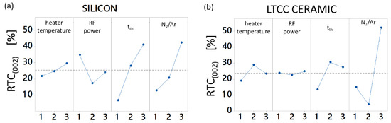
Figure 1.
Analysis of Means (ANOM) plot with relative texture coefficient (RTC)(002) as evaluation criterion (maximum optimization): (a) for silicon substrates; (b) for ceramic substrates.
The mean size of ordered domains d, which is related to grain size, was calculated for the respective strongest orientation using Scherrer method, see Equation (2) [33]:
In this equation, λ is the wavelength of copper radiation, β is the line broadening at half the maximum intensity, θ is the Bragg’s angle, and K a dimensionless shape factor, which was set to 1. These calculation results are also summarized in Table A1, Appendix B.
The real thickness of all layers was determined evaluating field emission scanning electron microscopy (FE-SEM) images, at a constant working distance of 8 mm, and acceleration voltages of 1.5 kV in all cases. The thickness results and respective real deposition rates are given in Table A1, Appendix B.
3. Results and Discussion
3.1. Influence of Process Parameters on Texture
Since a huge process range is investigated using a fractional factorial screening design, it is not possible to predict all influences. Thus, only evident trends will be highlighted in the following.
The process mean for the RTC value of the (002) orientation is 23.79% for layers deposited on ceramic substrates and 25.38% RTC(002) for layers deposited on silicon. The variance of the RTC evaluation amounts to 3%. ANOM results based on RTC(002) calculations are depicted in Figure 1a for silicon substrates and Figure 1b for ceramic substrates. Both charts differ significantly from each other. While the c-axis texture of the layers deposited on silicon increases strongly with increasing substrate temperature and thickness, the layers deposited on LTCC ceramic do not exhibit comparable behavior.
The ANOM plot reveals that, regardless of the substrate material, N2/Ar ratio has the strongest influence on the formation of a (002) texture, followed by tth. A clear increasing trend for these both parameters was observed for layers deposited on silicon, while the means of RTC(002) for layers deposited on ceramic show rising and falling tendencies as well. This fact is assumed to have its origin in the particular process conditions which occur using LTCC ceramic substrates at N2/Ar ratio of 5%. Although heater temperature and applied RF power have significant influence, which results from ANOVA, their effect on textured (002) growth is minor. Since nitrogen content in the atmosphere has a strong influence on arrival rate and incident energy of the adatoms, it affects the deposition rate significantly [34,35].
The real thickness differs significantly from the theoretical values, which are based on a rough estimation of the deposition rate, determined in preliminary attempts. These were carried out without substrate heating in pure argon atmosphere for 5 min. The real deposition rate changes significantly depending on RF power and N2/Ar ratio. These parameters effect an opposing trend: A nitrogen increase decreases the process mean of the deposition rate from 30 nm/s (pure argon) to 10 nm/s (10% N2/Ar), whereas an increase of the RF power increases the deposition rate from 10 nm/s (300 W) to 30 nm/s (500 W). A significant influence of heat temperature on the deposition rate could not be proven.
Summarizing all experiment results in Table A1, Appendix B, the best (002) texture was achieved in experiment #4 on ceramics with a N2/Ar ratio of 10%, heater temperature of 150 °C, RF power of 300 W, and a theoretical thickness of 1 µm. Since pronounced (002) orientation in the initial state is apparent in experiment #8 with only 670 nm thickness, it was repeated with prolonged deposition time in order to achieve thick layers with better (002) orientation (#10). Although this experiment leads to a high (002) texture, the RTC is still lower than that in experiment #4, which was performed with lower RF power and heater temperature. The lower deposition rate of 13 nm/s in this experiment and plasma interactions can cause this effect.
3.2. Layer Composition
Energy dispersive X-ray spectroscopy (EDX) (EDAX Element detector with Team-Software, 25 mm2, Si3N4 window, AMETEK Materials Analysis Division, AMETEK, Inc., Berwyn, PA, USA) was carried out at 15 kV acceleration voltage in order to determine the chemical composition. Samples coated in experiment #5, #7, and #10 were investigated as exemplary for the respective nitrogen content. Cross sections of the samples were prepared by grinding and coated with a 20 nm carbon layer in order to achieve sufficient conducting behavior. Aluminum and nitrogen content were measured on six points distributed over the layer. The ratio of the detected element concentration was evaluated. Mean value and standard deviation are depicted in Figure 2. The nitrogen content of the layer is distinguished significantly dependent on the substrate in #5 (0% N2). The nitrogen concentration of the layer deposited on the silicon is significantly lower than that deposited on the ceramic. Both layer present a clear substoichiometry between the Al and N. At higher nitrogen concentration (5% and 10%), the ratio trends towards a relation of 1:1. The deviation of measurements at 5% nitrogen content was very high. The EDX spectrum of all samples revealed the presence of oxygen. The oxygen incorporation in sputtered aluminum nitride is a known effect [2,6]. Its influence on functional properties must be studied in detail in further works.
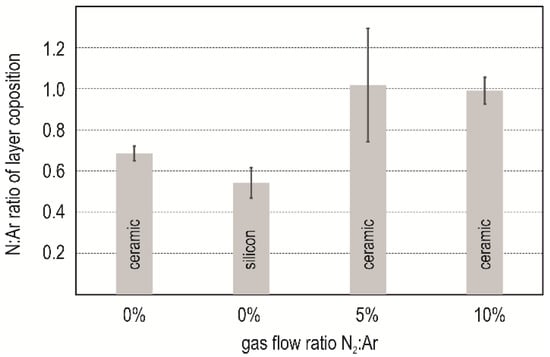
Figure 2.
Layer composition derived from energy dispersive X-ray spectroscopy (EDX) measurements.
3.3. Influence of Nitrogen to Argon Ratio on Morphology
3.3.1. Nitrogen to Argon Ratio 0%
All experiments carried out in poor nitrogen atmosphere produced layers with poor state of organization. The XRD patterns are shown in Figure 3. The thinnest layer deposited at room temperature (#1) has amorphous character. The others form cubic polycrystalline layers with hexagonal inclusions. The metastable cubic phase of aluminum nitride can be stabilized by none-equilibrium synthesis conditions [36,37], structural replication [38], and high stresses (pressures) [39].
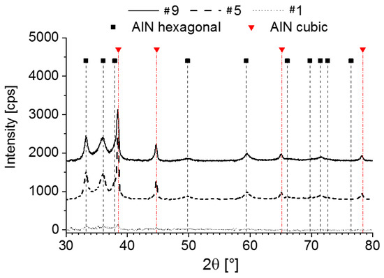
Figure 3.
X-ray diffraction (XRD) patterns of layers deposited in pure argon atmosphere on low temperature co-fired ceramic (LTCC).
Figure 4 depicts typical morphologic structures. Figure 4a,b show amorphous layers, deposited on silicon and ceramic. The thickness of the layer on ceramic is larger than that on silicon. On both substrates the layers appear densely with vermicular structures on top, originated from the aluminum excess during deposition. These features are of sub-stoichiometric aluminum rich composition [40]. Their size differs and they are larger when layers are deposited on LTCC. Figure 4c shows a pronounced example on ceramic. Comparing the layers in Figure 4d,e deposited in #9, the structure roots on ceramic start at a thickness of 3 µm approximately, while on silicon the initial dense layer is significantly thinner. Reference [40] confirms the relation between evident aluminum excess and occurrence of vermicular structures. Obtained layer are characterized by a high light absorption in the UV region. The relation between AlN stoichiometry and optical properties is studied in. An aluminum excess significantly affects refractive index and extinction coefficient. Accordingly, aluminum rich AlN can be used as absorbance layer in optical applications [2,41].
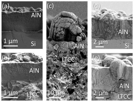
Figure 4.
Scanning electron microscope (SEM) micrographs of sputtered aluminum nitride (AlN) layer cross sections (N2:Ar = 0); (a) #1 on silicon; (b) #1 on ceramic; (c) #5 on ceramic; (d) #9 on silicon and (e) #9 on ceramic.
3.3.2. Nitrogen to Argon Ratio 5%
Consulting Figure 2 it can be assumed that at this deposition atmosphere the nitrogen saturation point necessary for stoichiometric composition is reached. It is known from the literature that small changes in the atmosphere affect deposition rate, layer structure, and morphology [35]. The deposition rate values in Table A1 have an unsteady characteristic.
Layer crystallinity is studied on the basis of #2 and #7, because #6 produced an amorphous layer. Figure 5 depicts SEM micrographs of the polycrystalline layers. They demonstrate the characteristic appearance of layers formed in the transition zone with densely packed fibrous grains, described by Thornton Modell [42]. Figure 5a,b compare samples deposited under the same conditions on silicon and ceramic. Both show a fine-grained column structure, but the columns on the silicon substrate are inclined and the layer has a significantly reduced thickness. The same inclination is observed in Figure 5c. This layer is deposited on ceramics at a significantly higher substrate temperature and at a lower deposition rate. The top view in Figure 5d reveals that the grains on top of the layer have triangular shape and the size is in the range of 200 nm.
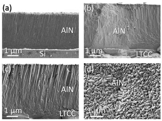
Figure 5.
SEM micrographs, samples sputtered with N2/Ar ratio of 5%: (a) #2 on silicon; (b) #2 on ceramic; (c) #7 on ceramic; (d) #7 top view on AlN (substrate ceramic).
The XRD patterns revealed several peaks. The peak intensity is depicted in the form of a bar chart of the calculated RTC values to provide a better clarity of the texture formation. Figure 6 compares experiment #2 and #7. The RTC distribution of the layer deposited in #2 on silicon, Figure 6a resembles this deposited on ceramic, Figure 6b. With decreasing deposition rate and increasing heater temperature #7, the deposition on silicon (Figure 6c) evolve (002) texture while those on ceramic (Figure 6d) are not significantly influenced by the process parameters.
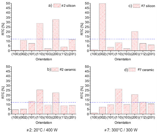
Figure 6.
Comparison of RTC distribution for layers sputtered with N2/Ar ratio of 5% on ceramic and silicon: (a) #2 (silicon); (b) #2 (ceramic); (c) #7 (silicon); (d) #7 (ceramic). The blue line indicates the RTC value that would represent a polycrystalline material of the respective measurement.
Despite the different heater temperature, RF power, deposition rate, and layer thickness in #2 and #7, similar crystal morphology arises on the different substrates (Figure 5a,c). Distribution of RTC (Figure 6a,d) and mean size of ordered domains (Table A1) are comparable as well, indicating that thermodynamic conditions at the substrate surface are similar.
3.3.3. Nitrogen to Argon Ratio 10%
The N2/Ar ratio of 10% provides the best deposition conditions for (002) textured layers in the investigated process range for both substrates. The deposition rate correlates with RF power. Figure 7 depicts the XRD patterns of layers deposited on ceramic. It reveals that the most pronounced (002) texture is achieved in #4 at a heater temperature of 150 °C and 400 W.
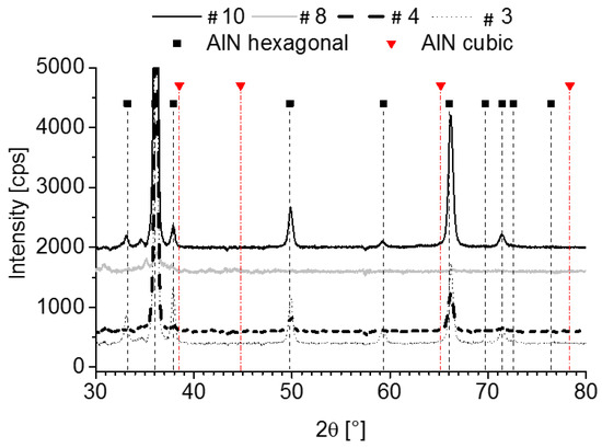
Figure 7.
XRD plots of layers deposited on ceramic at an N2/Ar ratio of 10%.
Figure 8 depicts cross sections of layers deposited on ceramic, the preparation of silicon samples failed because of the poor adherence. On all micrographs, an initial smooth layer at the substrate interface merges with a columnar structure. The thickness of this smooth transition layer varies. In Figure 8a (#3) the transition point starts at a thickness of 2 µm and in Figure 8b (#4) below 1 µm. In accordance with the RTC(002) values in Table A1, the columnar structure can be related to (002) texture. Figure 8c and d compare #8 and #10: The layer was deposited under same the condition, except the process time. The transition in Figure 8c starts at the 400 nm layer thickness, while in Figure 8d this zone is shifted to a thickness of almost 4 µm. Recrystallization can be accountable for this effect, supported by the fact that the mean size of the ordered domains increases from 14 nm to 24 nm. Along with this, the deposition rate rises. However, the desired increase of RTC(002) was not received. A more detailed experimental setup considering factor interactions will be carried out at this operation point in further works.
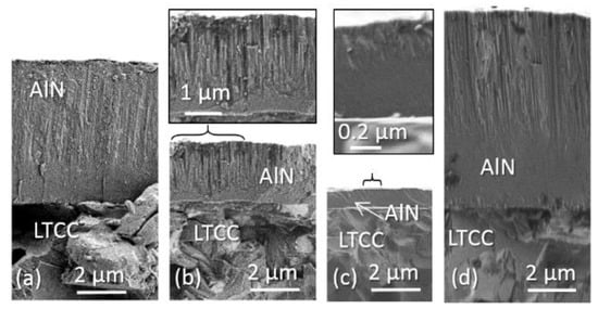
Figure 8.
SEM micrographs of layers deposited with N2/Ar ratio of 10% on LTCC: (a) #3; (b) #4; (c) #8; (d) #10.
3.4. Substrate Influence
3.4.1. Nucleation
Experiment #6 (tH 150 °C) allows a view on the starting grain growth on ceramic and silicon. The XRD pattern indicates an amorphous layer. On SEM images and corresponding AFM maps (Figure 9), commencing grain formation is visible. Nuclei size and distribution differ significantly depending on the substrate material. A dense distribution of fine seeds is visible on ceramic (Figure 9a). On silicon, the nuclei are larger and their distribution is sparse (Figure 9b). Experiment #1 (tH 20 °C) gives another example for the beginning nucleus formation. Crystallinity is still not detectable with XRD diffraction. Figure 10 depicts a top view on the layer surfaces; the difference between the seed structure is evident. While on silicon smaller nuclei are distributed with high density, on ceramic they are larger and less dense. These nuclei grow later to vermicular structures (compare Figure 4c). Despite of surface influence of the substrate, the thermal conditions undoubtedly play an important role.
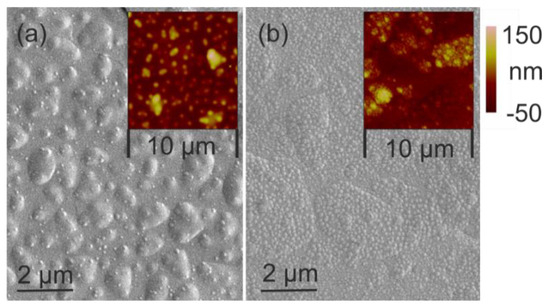
Figure 9.
SEM image and AFM-Plot of the sample surface in experiment #6: (a) silicon; (b) ceramic.
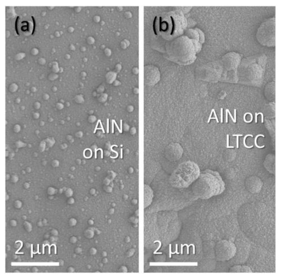
Figure 10.
SEM micrographs of initial nuclei in #1: (a) silicon; (b) ceramic.
3.4.2. Consideration of the Thermal Conditions
Thermal conditions on top of both substrates can be judged based on a rough calculation, using well-known physical relations of heat transport and storage. Since a part of the RF power produces heat at the substrate surface, the substrate temperature rises during the process. The total amount is not known, but the heat transport from the substrate surface to the substrate holder can be estimated. The rough calculation and the results can be found in Appendix C. This rough estimation shows, that the achievement of stable deposition conditions on ceramic substrates need a considerable longer time than those on silicon. Furthermore, the final temperature on LTCC ceramic surfaces is certainly higher than that at the silicon surface as a consequence of the higher thermal resistance. This leads to an apparent gradient of layer properties, which manifests in the grain structure change with increasing film thickness, see Figure 8a–d. Experiment #8 (Figure 8c) and #10 (Figure 8d) are deposited under the same conditions varying the process time. The beginning of the columnar structures is visibly shifted towards the thicker layers in experiment #10 and the main size of ordered domains d increases from 14 nm (#8) to 24 nm (#10). A further indication of higher substrate temperature on LTCC ceramic is the pronounced (002) texture observed in experiment #4 in comparison to silicon.
3.4.3. Layer Stress
Visual inspection and SEM image analysis were the base of the adhesion’s assessment. Peeled off layers were assessed with “−“, layers with cracks and chipping with “−“, well adherent layers with cracks with “+” and excellent adhered layers without cracks with “++”. The results are listed in Table A1, Appendix B. The layer adhesion on ceramic is excellent, in the sense that no cracks were detected, there were no areas in which the top layer was peeled off the ceramic, and SEM indicated a substrate/layer interface without voids. In comparison, the adhesion is partially poor on silicon. Here, only the thin layer adheres well, while the thicker layer possess cracks at the interface between the substrate and layer, or chipping. Particularly those layers deposited under high nitrogen content showed poor adhesion. In the case of experiment #10, the layer is fully peeled off from the silicon substrate, indicating high stress.
The layer stress can be estimated from the deviation between measured crystal parameters (extracted from XRD pattern) and theoretical values. The lattice expansion εx, εy in the respective direction in plane was calculated using Equation (3):
Here, a0 is the theoretical constant of a non-deformed layer and a constant of the real layer, extracted from the XRD pattern. The value for a0 is 3.112 Å [43]. The expansion εz perpendicular to the plane was calculated using Equation (4):
Here, cij stands for the elastic constants in the respective direction relating to substrate surface, where i, j = 1,2 or 3, for x, y or z directions, respectively. The respective tensions σ were calculated using Equation (5) for tension in plane:
and Equation (6) for tensions perpendicular to the plane:
The variation of the stress values was estimated on the basis of three independent measurements on equal layers and amounts to 3%. Amorphous layers or such with only weak orientation cannot be evaluated. This concerns experiment #1, #6, and #8. Table A1 summarizes all other values and Figure 11 compares them graphically.
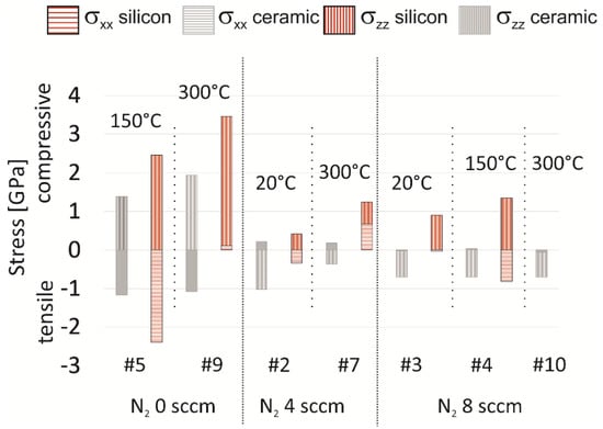
Figure 11.
Layer stress depending on substrate material, ordered by gas atmosphere and heater temperature.
The resulting stress superposes internal stress generated by layer growth (intrinsic) and thermal stress generated by thermal mismatch between substrate and layer (extrinsic). Lattice mismatch, grain boundary effects, and lattice defects cause intrinsic stress.
In the current experiment, no significant influence of RF power and thickness on layer stress is apparent. A clear difference between the resulting stress of layers deposited on ceramic and silicon is evident and due to the reduction of the extrinsic stress component for the LTCC substrate having a lower thermal mismatch to AlN. As pointed out in Figure 11, the stress σxx in plane for layers deposited on ceramic substrates mainly depends on nitrogen content. The heater temperature has no significant influence. Layers deposited with nitrogen content of 10% show absolute stress lower than 60 MPa (both, tensile and compressive). The stress perpendicular to the substrate plane σzz has compressive character at low nitrogene content and turns over to tensile character at higher nitrogen content. Independently from heater temperature, it reaches values around 700 MPa tensile strain when the N2/Ar gas flow ratio is 10%.
Layers deposited on silicon evince a significantly different behavior. Besides the nitrogen content influence, both stress components, σxx in plane and σzz perpendicular, depend strongly on heater temperature as well. Increasing heater temperature leads to a shift of the in plane stress σxx towards a compressive character. It turns to tensile for layers deposited at high nitrogen content and reaches a value of 810 MPa tensile stress. The perpendicular stress components have compressive character and their variation with the heater temperature is low. The comparison of the process means in Figure 12 reveals that mean of real values (obtained from signed values) as well as mean of absolute value is lower when the layers are deposited on LTCC substrates. This pertains to stress in the basal plane and the perpendicular as well, independent from the process conditions.
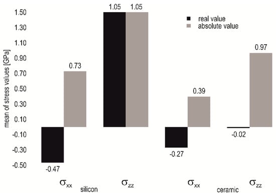
Figure 12.
Comparison of the process means based on real and absolute stress value on silicon and ceramic substrate.
4. Conclusions
The deposition of aluminum nitride on silicon and LTCC ceramic was investigated over a wide parameter range using RF magnetron sputtering. The N2/Ar ratio has the most significant influence on all investigated characteristics, due to a variation of the layer composition. The nitrogen content of the layers increases strongly with rising N2/Ar ratio from 0% to 5%. At 5% N2/Ar ratio, saturation occurs. Layers deposited under an atmosphere with 10% N2/Ar ratio show stoichiometric composition.
The effect of process parameter change, including heater temperature, RF power, N2/Ar ratio and targeted thickness, on layer morphology depends strongly on the substrate material. Different thermal properties leading to dissimilar surface temperatures and heat-up performance are an essential reason for this. Stable deposition conditions on LTCC ceramic need considerable longer time. Since a high heat amount emerges during the sputtering process, the surface temperature on the LTCC ceramic substrate is higher than that on silicon because of a two order of magnitude higher thermal resistance. Due to these circumstances, the nucleation differs significantly in dependence on the substrate material and layer formation continues differently. Thus, the process conditions for c-axis oriented AlN layer deposition vary significantly dependent on the substrate. Best (002) texture is achieved on ceramic substrates at a heater temperature of 150 °C and RF power of 300 W.
The use of CTE adapted LTCC substrates leads to a significant stress reduction. Since stress caused by CTE mismatch is minimized, resulting components are mainly produced by internal factors, such as lattice defects or grain boundary influences. Very low stress of 60 MPa (tensile and compressive as well) is achieved in the basal plane. The use of ceramic substrates with adapted coefficient of thermal expansion enables thus a targeted process development, producing layers with application tailored properties whose characteristics are not restricted by stress compensating needs affecting functional properties.
Supplementary Materials
The following are available online at http://www.mdpi.com/2079-6412/8/8/289/s1, Figure S1: XRD patterns of all samples, sputtered on ceramic, Figure S2: XRD patterns of all samples, sputtered on silicon, Figure S3: RTC calculations for all experiments, samples prepared on ceramics, Figure S4: RTC calculations for all experiments, samples prepared on silicon.
Author Contributions
Conceptualization, H.B. and J.P.; Methodology, R.G. (XRD), H.B. (DoE), Jö.M. (SEM, AFM); Resources, Je.M.; Writing—Original Draft Preparation, H.B.; Writing—Review & Editing, H.B., Jö.M., J.P., R.G.; Project Administration, H.B.; Funding Acquisition, Je.M.
Funding
This research was funded by the Alexander von Humboldt Foundation, through the “Humboldt Research Fellowship for Postdoctoral Researchers Program” (Ref. 3.3-1 1S8421-ES-HFST-P) and from the German Federal Ministry for Economic Affairs (BMWi) within the project “BiSWind, Integrated Sensor Technolgies for Wind Turbines” (Ref. 0325891B).
Acknowledgments
The authors would like to thank Ulrike Brokmann for her support at AFM and Peter Schaaf, who kindly provided the access to the analytical equipment. We acknowledge support for the Article Processing Charge by the German Research Foundation and the Open Access Publication Fund of the Technische Universität Ilmenau.
Conflicts of Interest
The authors declare no conflict of interest.
Appendix A
The ceramic substrates are lapped with cubic B4C slurry for 20 min and polished for 90 min using diamond slurry with 1 µm grain size. The final substrate thickness was 0.9 mm. The roughness of the polished areas is measured using laser scanning microscopy (LSM) and atomic force microscopy (AFM). Figure A1a shows a LSM image and Figure A1b an AFM scan.

Figure A1.
Surface topography of a polished LTCC ceramic substrate, captured by (a) laser scanning microscopy (LSM); (b) atomic force microscopy (AFM) beside pores.
The LSM (OLS 4100, Olympus, Hamburg, Germany) has a spot size of 200 nm. Surface scans were carried out over 130 µm × 130 µm (field of view) on 9 substrates. The roughness of the whole substrate area including pores was obtained from the primary data after applying a filter with a cut-off length of 8 µm. Root mean square height of the surface Sq is evaluated using the device software OLS4100 (Version). The results Sq (LSM) are depicted in Figure A2. Three of these LSM surface scans were chosen and 6-line scans along closed polished areas were evaluated to obtain root mean square roughness Rrms of non-porous regions as illustrated in Figure A1a. Figure A2 presents the obtained values Rq (LSM). The cut-off length for this evaluation amounts to 2.5 µm. As a third parameter, the portion of pores, was calculated on the base of the LSM surface scans. The threshold was defined at a level of 300 nm underneath the maximum values of the topography. All regions lower than the threshold were interpreted as pore. The obtained porosity is 23% and the standard deviation is 5%.
Additionally, AFM scans (VECCO AFM measurements, Veeco Instruments Inc., Plainview, NY, USA) were carried out on regions with an area of 1.4 µm × 1.4 µm. As indicated in Figure A1a, regions without pores were selected. The obtained Sq values base on seven measurements, Figure A2 depicts the values in under category Sq (AFM).

Figure A2.
Surface parameter obtained from LSM and AFM.
Appendix B

Table A1.
Summary of experimental design and results.
Table A1.
Summary of experimental design and results.
| Exp. No. | Set Point | Measured results | RTC(002) | |||||
| Heater Temperature [°C] | RF Power [W] | Targeted Thickness [µm] | Nitrogen Gas Flow [sccm] | Rate [nm min−1] | Thickness [nm] | Si | 9k7 | |
| 1 b | 20 | 300 | 0.3 | 0 | 8 | 1400 | n.a. | n.a. |
| 2 | 20 | 400 | 1 | 4 | 27 | 3500 | 12 | 5 |
| 3 | 20 | 500 | 1.7 | 8 | 25 | 4300 | 53 | 52 |
| 4 | 150 | 300 | 1 | 8 | 13 | 2400 | 54 | 64 |
| 5 a | 150 | 400 | 1.7 | 0 | 31 | 6000 | 19 | 22 |
| 6 b | 150 | 500 | 0.3 | 4 | 22 | 700 | n.a. | n.a. |
| 7 | 300 | 300 | 1.7 | 4 | 18 | 5200 | 50 | 7.5 |
| 8 | 300 | 400 | 0.3 | 8 | 17 | 670 | 20 | 40 |
| 9 a | 300 | 500 | 1 | 0 | 43 | 4500 | 18 | 22 |
| 10 | 300 | 400 | 1.7 | 8 | 23 | 7100 | n.a. | 60 |
| Exp. No. | Mean size of Ordered Domains d | Stress [GPa] | Adhesion | |||||
| Si | 9k7 | Si | 9k7 | |||||
| Si [nm] | 9k7 [nm] | σxx | σzz | σxx | σzz | |||
| 1 b | n.a. | n.a. | n.a. | n.a. | n.a. | n.a. | + | ++ |
| 2 | 19(200) | 21(110) | −0.34 | 0.41 | 0.21 | −1.03 | − | ++ |
| 3 | 27 | 24 | −0.03 | 0.90 | −0.02 | −0.69 | − | ++ |
| 4 | 23 | 23 | −0.81 | 1.34 | 0.04 | −0.71 | − | ++ |
| 5 a | 13 b | 12 b | −2.40 | 2.46 | −1.17 | 1.39 | − | ++ |
| 6 b | n.a. | n.a. | n.a. | n.a. | n.a. | n.a. | ++ | ++ |
| 7 | 26 | 22(110) | 0.67 | 0.57 | 0.18 | −0.37 | − | ++ |
| 8 | 30(112) | 14 | n.a. | n.a. | n.a. | n.a. | ++ | ++ |
| 9 a | 8 c | 13 c | 0.10 | 3.35 | −1.08 | 1.94 | + | ++ |
| 10 | n.a. | 24 | n.a. | n.a. | −0.06 | −0.64 | − − | ++ |
Notes: a (111) cubic orientation dominant; b amorphous layer; c RTC(111) cubic; d (002) hexagonal if not specified; − − peel off; − cracks and chipping; + well adhesion, cracks at the substrate-layer-interface; ++ excellent adhesion, no cracks.
Appendix C
The rough calculation of thermal conditions bases on the consideration of an area element on the respective substrate. Figure A3 illustrates the conditions. With the beginning sputtering process, heat is generated on the substrate surface by ion bombardment. The generated heat is dissipated through the substrate towards the substrate holder. Thermal resistivity Rth and heat capacitance Cth of the substrate characterize the heat flow.

Figure A3.
Thermal conditions and geometric parameters determining the heat dissipation: Tsurface—temperature at the substrate surface; Tholder—temperature at the substrate holder; th—substrate thickness.
Rth is calculated using Equation (A1):
The presumed thermal conductivity kth of the substrates is 150 W m−1 K−1 for silicon [44] and 3.3 W m−1 K−1 for ceramic [45]. Considering the different substrate thickness th of 0.5 mm (silicon) and 0.9 mm (ceramic), Rth of a representative area element A of 1 mm2 amounts to 3.3 KW−1 for silicon and 273 KW−1 for ceramics. Cth of the substrates can be calculated using Equation (A2):
csp is the specific thermal capacity. It can be experimentally determined or calculated using Equation (A3):
where kth is the specific thermal conductivity in W m−1 K−1, α represents the thermal diffusivity in m2 s−1 and is the density in kg m−3.
Reliable data csp for the LTCC material are not available. Since LTCC ceramics are a composite of different glasses and ceramic fillers, the specific heat capacity is roughly estimated as a 1:1 mixture of alumina as frequently used ceramic filler and glass. Reference [46] specifies the csp of glasses to be 850 J kg−1 K−1 with a tolerance of 10%. Other internet sources specify values between 503 J kg−1 K−1 (lead glass, [47]) and 720–800 J kg−1 K−1 (soda lime glass, [48]). Values for silicon vary from 703 J kg−1 K−1 [49] to 741 J kg−1 K−1 [50]. For alumina, sources specify 990 J kg−1 K−1 [51] and 850–1050 J kg−1 K−1 [52]. The calculation of csp based on thermal diffusivity (Equation (A3)) is an alternative way to obtain data. Necessary material constants are gathered in Table A2.
Table A2.
Thermal material data for silicon, alumina and lead oxide.
Table A2.
Thermal material data for silicon, alumina and lead oxide.
| Material | kth (W/mK) | α (10−6 m2/s) | (103 kg/m3) |
|---|---|---|---|
| Silicon | 156 [53] ~150 [44] | 88.0 [54,55] 76.9 [56] | 2.329002 [57] |
| Alumina | 36.96 [58] 30.5 * [59] | 12 [58] 13.7 [56] | 3.48 * [59] |
Notes: * sintered alumina at 881.7 °C (k values change also with this T), open pores 10.65%, closed pores 2.35%
The calculated heat capacity based on these data for silicon and alumina results in the data range presented in Table A3.
Table A3.
Data calculated using Equation (A3) for silicon and alumina.
Table A3.
Data calculated using Equation (A3) for silicon and alumina.
| Material | min | csp [J kg−1] average | max |
|---|---|---|---|
| Silicon | 761 | 816 | 871 |
| Alumina | 640 | 710 | 781 |
Considering calculated values for csp and those found in the literature, a minimum-maximum assessment for Cth was carried out. These valued and resulting time constant τ and period 5τ considering the above calculated thermal resistance are presented in Table A4, whereby the time constant is calculated with Equation (A4):
τ = Rth × Cth
Table A4.
Calculated values for Cth using Equation (A2), based on different csp values.
Table A4.
Calculated values for Cth using Equation (A2), based on different csp values.
| Specific Heat Capacity Csp [J kg−1 K−1] | Cth | τ [s] | 5τ [s] | 5τ [min] | ||
|---|---|---|---|---|---|---|
| Si | – | – | – | – | ||
| 871 | 1.017 | 3.4 | 17 | 0.3 | ||
| 703 | 0.821 | 2.7 | 13.7 | 0.2 | ||
| Alumina | glass | ceramic * | ||||
| 990 | 800 | 895 | 2.497 | 681 | 3405 | 57 |
| 640 | 503 | 571 | 1.594 | 435 | 2174 | 36 |
Notes: * value of the composite ceramic results from the mean of Al2O3 and glass.
Despite of huge deviations due to the uncertainty of material data, it is evident that the time constant τ of the ceramic substrate is significantly higher than that of silicon. The thermal resistance, which amounts to 3.3 KW−1 for silicon and 273 KW−1 for ceramic, has the strongest influence. As a consequence, the silicon substrate reaches the steady state in a few seconds and the heat rapidly dissipated. The ceramic substrate accumulates the heat; it can take up to an hour until the steady state is reached.
References
- Khoshman, J.M.; Kordesch, M.E. Optical characterization of sputtered amorphous aluminum nitride thin films by spectroscopic ellipsometry. J. Non-Cryst. Solids 2005, 351, 3334–3340. [Google Scholar] [CrossRef]
- Zhao, S.; Wäckelgård, E. The optical properties of sputtered composite of Al–AlN. Sol. Energy Mater. Sol. Cells 2006, 90, 1861–1874. [Google Scholar] [CrossRef]
- Oikawa, H.; Akiyama, R.; Kanazawa, K.; Kuroda, S.; Harayama, I.; Nagashima, K.; Sekiba, D.; Ashizawa, Y.; Tsukamoto, A.; Nakagawa, K.; et al. Deposition and characterization of amorphous aluminum nitride thin films for a gate insulator. Thin Solid Films 2015, 574, 110–114. [Google Scholar] [CrossRef]
- Harris, H.; Biswas, N.; Temkin, H.; Gangopadhyay, S.; Strathman, M. Plasma enhanced metalorganic chemical vapor deposition of amorphous aluminum nitride. J. Appl. Phys. 2001, 90, 5825–5831. [Google Scholar] [CrossRef]
- Piazza, G.; Felmetsger, V.; Muralt, P.; Olsson III, R.H.; Ruby, R. Piezoelectric aluminum nitride thin films for microelectromechanical systems. MRS Bull. 2012, 37, 1051–1061. [Google Scholar] [CrossRef]
- Hou, Y.; Zhang, M.; Han, G.; Si, C.; Zhao, Y.; Ning, J. A review: Aluminum nitride MEMS contour-mode resonator. J. Semicond. 2016, 37, 101001. [Google Scholar] [CrossRef]
- Lee, J.W.; Cuomo, J.J.; Cho, Y.S.; Keusseyan, R.L. Aluminum nitride thin films on an LTCC Substrate. J. Am. Ceram. Soc. 2005, 88, 1977–1980. [Google Scholar] [CrossRef]
- Tadigadapa, S.; Mateti, K. Piezoelectric MEMS sensors: State-of-the-art and perspectives. Meas. Sci. Technol. 2009, 20, 092001. [Google Scholar] [CrossRef]
- Cimalla, V.; Pezoldt, J.; Ambacher, O. Group III nitride and SiC based MEMS and NEMS: Materials properties, technology and applications. J. Phys. D Appl. Phys. 2007, 40, 6386–6434. [Google Scholar] [CrossRef]
- Lin, C.-M.; Chen, Y.-Y.; Felmetsger, V.V.; Lien, W.-C.; Riekkinen, T.; Senesky, D.G.; Pisano, A.P. Surface acoustic wave devices on AlN/3C-SiC/Si multilayer structures. J. Micromech. Microeng. 2013, 23, 025019. [Google Scholar] [CrossRef]
- Di Pietrantonio, F.; Benetti, M.; Cannata, D.; Beccherelli, R.; Verona, E. Guided lamb wave electroacoustic devices on micromachined AlN/Al plates. IEEE Trans. Ultrason. Ferroelectr. Freq. Control 2010, 57, 1175–1182. [Google Scholar] [CrossRef] [PubMed]
- Xiong, C.; Pernice, W.H.P.; Sun, X.; Schuck, C.; Fong, K.Y.; Tang, H.X. Aluminum nitride as a new material for chip-scale optomechanics and nonlinear optics. New J. Phys. 2012, 14, 95014. [Google Scholar] [CrossRef]
- Khelif, A.; Wilm, M.; Laude, V.; Ballandras, S.; Djafari-Rouhani, B. Guided elastic waves along a rod defect of a two-dimensional phononic crystal. Phys. Rev. E 2004, 69, 067601. [Google Scholar] [CrossRef] [PubMed]
- Panda, P.; Ramaseshan, R.; Ravi, N.; Mangamma, G.; Jose, F.; Dash, S.; Suzuki, K.; Suematsu, H. Reduction of residual stress in AlN thin films synthesized by magnetron sputtering technique. Mater. Chem. Phys. 2017, 200, 78–84. [Google Scholar] [CrossRef]
- Mehner, H.; Leopold, S.; Hoffmann, M. Variation of the intrinsic stress gradient in thin aluminum nitride films. J. Micromech. Microeng. 2013, 23, 095030. [Google Scholar] [CrossRef]
- Gongora-Rubio, M.R.; Espinoza-Vallejos, P.; Sola-Laguna, L.; Santiago-Avilés, J.J. Overview of low temperature co-fired ceramics tape technology for meso-system technology (MsST). Sens. Actuators A 2001, 89, 222–241. [Google Scholar] [CrossRef]
- Khoong, L.E.; Tan, Y.M.; Lam, Y.C. Overview on fabrication of three-dimensional structures in multi-layer ceramic substrate. J. Eur. Ceram. Soc. 2010, 30, 1973–1987. [Google Scholar] [CrossRef]
- Yang, J.; Wang, Z. LTCC Substrates for RF/MW Application. In RF and Microwave Microelectronics Packaging; Kuang, K., Kim, F., Cahill, S.S., Eds.; Springer: Boston, MA, USA, 2010; pp. 189–206. [Google Scholar]
- Ariza, A.P.G.; Muller, R.; Wollenschlager, F.; Schulz, A.; Elkhouly, M.; Sun, Y.; Glisic, S.; Trautwein, U.; Stephan, R.; Muller, J.; et al. 60 GHz ultrawideband polarimetric MIMO sensing for wireless multi-gigabit and radar. IEEE Trans. Antennas Propagat. 2013, 61, 1631–1641. [Google Scholar] [CrossRef]
- Ullah, U.; Mahyuddin, N.; Arifin, Z.; Abdullah, M.Z.; Marzuki, A. Antenna in LTCC technologies: A review and the current state of the art. IEEE Antennas Propag. Mag. 2015, 57, 241–260. [Google Scholar] [CrossRef]
- Kobe, O.B.; Chuma, J.; Jamisola, R.; Chose, M. A review on quality factor enhanced on-chip microwave planar resonators. Eng. Sci. Technol. 2017, 20, 460–466. [Google Scholar] [CrossRef]
- Ma, M.; Khan, H.; Shan, W.; Wang, Y.; Ou, J.Z.; Liu, Z.; Kalantar-zadeh, K.; Li, Y. A novel wireless gas sensor based on LTCC technology. Sens. Actuators B 2017, 239, 711–717. [Google Scholar] [CrossRef]
- Sobocinski, M.; Bilby, D.; Kubinski, D.; Visser, J.; Andersson, M.; Juuti, J.; Spetz, A.L.; Jantunen, H. SiC MOSFET soot sensor in a co-fired LTCC package. Proced. Eng. 2016, 168, 27–30. [Google Scholar] [CrossRef]
- Maeder, T.; Jacq, C.; Testa, D.; Toussaint, M.; Stöck, M.; Corne, A.; Güniat, L.; Ellenrieder, B.; Jiang, X.; Windischhofer, P.; et al. LTCC and thick-film ceramic magnetic sensors for tokamak nuclear fusion. Proced. Eng. 2016, 168, 646–649. [Google Scholar] [CrossRef]
- Higuchi, Y.; Sugimoto, Y.; Harada, J.; Tamura, H. LTCC system with new high-ɛr and high-Q material co-fired with conventional low-ɛr base material for wireless communications. J. Eur. Ceram. Soc. 2007, 27, 2785–2788. [Google Scholar] [CrossRef]
- Sebastian, M.T.; Jantunen, H. Low loss dielectric materials for LTCC applications: A review. Int. Mater. Rev. 2008, 53, 57–90. [Google Scholar] [CrossRef]
- Müller, J.; Perrone, R.; Drüe, K.-H.; Stephan, R.; Trabert, J.; Hein, M.; Schwanke, D.; Pohlner, J.; Reppe, G.; Kulke, R.; et al. Comparison of high-resolution patterning technologies for LTCC microwave circuits. J. Microelectron. Electron. Packag. 2007, 4, 99–104. [Google Scholar] [CrossRef]
- Bittner, A.; Ababneh, A.; Seidel, H.; Schmid, U. Influence of the crystal orientation on the electrical properties of AlN thin films on LTCC substrates. Appl. Surf. Sci. 2010, 257, 1088–1091. [Google Scholar] [CrossRef]
- Yim, W.M.; Paff, R.J. Thermal expansion of AlN, sapphire, and silicon. J. Appl. Phys. 1974, 45, 1456–1457. [Google Scholar] [CrossRef]
- Gutzeit, N.; Fischer, M.; Bartsch, H.; Müller, J. Lapping and polishing of different LTCC substrates for thin film applications. In Proceedings of the 2015 European Microelectronics Packaging Conference (EMPC), Friedrichshafen, Germany, 14–16 September 2015; pp. 1–4. [Google Scholar]
- Bengoa, L.N.; Tuckart, W.R.; Zabala, N.; Prieto, G.; Egli, W.A. Tin coatings electrodeposited from sulfonic acid-based electrolytes: Tribological behavior. J. Mater. Eng. Perform. 2015, 24, 2274–2281. [Google Scholar] [CrossRef]
- Camargo, M.K.; Schmidt, U.; Grieseler, R.; Wilke, M.; Bund, A. Electrodeposition of Zn-TiO2 dispersion coatings: Study of particle incorporation in chloride and sulfate baths. J. Electrochem. Soc. 2014, 161, D168–D175. [Google Scholar] [CrossRef]
- Mittemeijer, E.J.; Welzel, U. Modern Diffraction Methods; Wiley-VCH Verlag GmbH & Co. KGaA: Weinheim, Germany, 2012. [Google Scholar]
- Cheng, H.; Sun, Y.; Zhang, J.X.; Zhang, Y.B.; Yuan, S.; Hing, P. AlN films deposited under various nitrogen concentrations by RF reactive sputtering. J. Cryst. Growth 2003, 254, 46–54. [Google Scholar] [CrossRef]
- Cho, S. Effect of nitrogen flow ratio on the structural and optical properties of aluminum nitride thin films. J. Cryst. Growth 2011, 326, 179–182. [Google Scholar] [CrossRef]
- Lin, W.T.; Meng, L.C.; Chen, G.J.; Liu, H.S. Epitaxial growth of cubic AlN films on (100) and (111) silicon by pulsed laser ablation. Appl. Phys. Lett. 1995, 66, 2066–2068. [Google Scholar] [CrossRef]
- Kim, Y.H.; Kim, C.S.; Noh, Y.K.; Kim, M.D.; Oh, J.E. Substrate temperature dependence of the phase transition behavior of AlN layers grown on Si(111) substrate by metalorganic chemical vapor deposition. J. Cryst. Growth 2011, 334, 189–194. [Google Scholar] [CrossRef]
- Lebedev, V.; Cimalla, V.; Kaiser, U.; Foerster, C.; Pezoldt, J.; Biskupek, J.; Ambacher, O. Effect of nanoscale surface morphology on the phase stability of 3C-AlN films on Si(111). J. Appl. Phys. 2005, 97, 114306. [Google Scholar] [CrossRef]
- Johnson, G.R.; Holmquist, T.J.; Beissel, S.R. Response of aluminum nitride (including a phase change) to large strains, high strain rates, and high pressures. J. Appl. Phys. 2003, 94, 1639–1646. [Google Scholar] [CrossRef]
- Zang, Y.; Li, L.; Ren, Z.; Cao, L.; Zhang, Y. Characterization of AlN thin film prepared by reactive sputtering. Surf. Interface Anal. 2016, 48, 1029–1032. [Google Scholar] [CrossRef]
- Yuan, Q.; Döll, J.; Romanus, H.; Wang, H.; Bartsch, H.; Albrecht, A.; Hoffmann, M.; Schaaf, P.; Wang, D. Surface-nanostructured Al-AlN composite thin films with excellent broad-band antireflection properties fabricated by limited reactive sputtering. ACS Appl. Nano Mater. 2018, 1, 1124–1130. [Google Scholar] [CrossRef]
- Thornton, J.A. High rate thick film growth. Ann. Rev. Mater. Sci. 1977, 7, 239–260. [Google Scholar] [CrossRef]
- Ambacher, O.; Smart, J.; Shealy, J.R.; Weimann, N.G.; Chu, K.; Murphy, M.; Schaff, W.J.; Eastman, L.F.; Dimitrov, R.; Wittmer, L.; et al. Two-dimensional electron gases induced by spontaneous and piezoelectric polarization charges in N- and Ga-face AlGaN/GaN heterostructures. J. Appl. Phys. 1999, 85, 3222–3233. [Google Scholar] [CrossRef]
- Childs, G.E.; Ericks, L.J.; Powell, R.L. Thermal Conductivity of Solids at Room Temperature and Below: A Review and Compilation of the Literature; U.S. Department of Commerce, National Bureau of Standards: Olympia, WA, USA, 1973.
- DuPontTM GreenTapeTM 9k7 Low Temperature Co-fired Ceramic Material System. Available online: http://www.dupont.com/products-and-services/electronic-electrical-materials/low-temperature-co-fire-ceramic-materials/brands/greentape-ceramic-circuit/products/green-tape-9k7-ltcc-material-system.html (accessed on 16 August 2018).
- Nölle, G. Technik der Glasherstellung; Wiley-VCH: Weinheim, Germany, 2009. (In German) [Google Scholar]
- LUMITOS GmbH, Berlin, Germany. Spezifische Wärmekapazität. Available online: http://www.chemie.de/lexikon/Spezifische_W%C3%A4rmekapazit%C3%A4t.html (accessed on 11 July 2018).
- Soda-Lime (Float) Glass. Available online: https://www.makeitfrom.com/material-properties/Soda-Lime-Float-Glass/ (accessed on 11 July 2018).
- Binder, H.H. Lexikon der chemischen Elemente. Das Periodensystem in Fakten, Zahlen und Daten; Hirzel: Stuttgart, Germany, 1999. (In German) [Google Scholar]
- Wikimedia Foundation Inc. Wikibooks: Tabellensammlung Chemie/Spezifische Wärmekapazitäten. Available online: https://de.wikibooks.org/wiki/Tabellensammlung_Chemie/_spezifische_W%C3%A4rmekapazit%C3%A4ten (accessed on 12 July 2018).
- Al2O3 Aluminiumoxid Technische Hochleistungskeramik. Available online: https://www.pgo-online.com/de/al2o3.html (accessed on 12 July 2018).
- HiDur® Aluminiumoxid-Kugeln. Available online: http://www.rvtpe.com/wp-content/uploads/2013/06/Kugeln-Aluminiumoxid.pdf (accessed on 12 July 2018).
- Glassbrenner, C.J.; Slack, G.A. Thermal conductivity of silicon and germanium from 3°K to the melting point. Phys. Rev. 1964, 134, A1058–A1069. [Google Scholar] [CrossRef]
- ASTM E1461-01 Standard Test Method for Thermal Diffusivity of Solids by the Flash Method; ASTM International: West Conshohocken, PA, USA, 2001.
- King, J. Material Handbook for Hybrid Microelectronics; Artec House: Washington, DC, USA, 1988. [Google Scholar]
- Touloukian, Y.S.; Powell, R.W.; Ho, C.Y.; Klemens, P.G. Thermophysical Properties of Matter; IFI/Plenum Data Corp.: New York, NY, USA; Washington, DC, USA, 1970. [Google Scholar]
- Henins, I. Precision Density Measurement of Silicon. J. Res. Natl. Bur. Stand. A Phys. Chem. 1964, 68A, 529–533. [Google Scholar] [CrossRef]
- Touloukian, Y.S. Thermophysical Properties of High Temperature Solid Materials; Macmillan: New York, NY, USA, 1967. [Google Scholar]
- Touloukian, Y.S.; Powell, R.W.; Ho, C.Y.; Klemens, P.G. Thermophysical Properties of Matter. Thermal Conductivity; IFI/Plenum Data Corp.: New York, NY, USA; Washington, DC, USA, 1970. [Google Scholar]
© 2018 by the authors. Licensee MDPI, Basel, Switzerland. This article is an open access article distributed under the terms and conditions of the Creative Commons Attribution (CC BY) license (http://creativecommons.org/licenses/by/4.0/).