Article

Electrostatic Supercapacitors by Atomic Layer Deposition on Nanoporous Anodic Alumina Templates for Environmentally Sustainable Energy Storage

by
Luis Javier Fernández-Menéndez
1,*,
Ana Silvia González
1,
Víctor Vega
1,2 and
Víctor Manuel De la Prida
1,*
1
Departamento de Física, Facultad de Ciencias, Universidad de Oviedo, C/Federico García Lorca n° 18, 33007 Oviedo, Asturias, Spain
2
Laboratorio de Membranas Nanoporosas, Edificio de Servicios Científico Técnicos “Severo Ochoa”, Universidad de Oviedo, C/Fernando Bonguera s/n, 33006 Oviedo, Asturias, Spain
*
Authors to whom correspondence should be addressed.
Coatings 2018, 8(11), 403; https://doi.org/10.3390/coatings8110403
Submission received: 24 September 2018 / Revised: 31 October 2018 / Accepted: 10 November 2018 / Published: 14 November 2018
(This article belongs to the Special Issue Atomic Layer Deposition)

Abstract

:
In this work, the entire manufacturing process of electrostatic supercapacitors using the atomic layer deposition (ALD) technique combined with the employment of nanoporous anodic alumina templates as starting substrates is reported. The structure of a usual electrostatic capacitor, which comprises a top conductor electrode/the insulating dielectric layer/and bottom conductor electrode (C/D/C), has been reduced to nanoscale size by depositing layer by layer the required materials over patterned nanoporous anodic alumina membranes (NAAMs) by employing the ALD technique. A thin layer of aluminum-doped zinc oxide, with 3 nm in thickness, is used as both the top and bottom electrodes’ material. Two dielectric materials were tested; on the one hand, a triple-layer made by a successive combination of 3 nm each layers of silicon dioxide/titanium dioxide/silicon dioxide and on the other hand, a simple layer of alumina, both with 9 nm in total thickness. The electrical properties of these capacitors are studied, such as the impedance and capacitance dependences on the AC frequency regime (up to 10 MHz) or capacitance (180 nF/cm2) on the DC regime. High breakdown voltage values of 60 V along with low leakage currents (0.4 μA/cm2) are also measured from DC charge/discharge RC circuits to determine the main features of the capacitors behavior integrated in a real circuit.

Graphical Abstract

1. Introduction

Society is increasingly aware of the usage of sustainable energy sources that protect the environment, such as renewable energy resources, whose viability is demonstrated. At the same time, it is necessary that energy storage devices also meet the same requirements of sustainability and efficiency, making the entire process of generation and consumption of energy as clean as possible. Nanotechnology has become one of the main subjects in science nowadays, offering exciting new possibilities in the field of renewable energy production/conversion and storage. An energy storage device is characterized by two main magnitudes. The first one is the energy density, which gives an account of the total energy that the device could store. The other magnitude refers to the time necessary for the device to store or supply a certain amount of energy to attend to the demand, which is known as power density.
Within storage systems, capacitors are those that have higher power densities, but the lowest energy density. Supercapacitors, apart from maintaining the power density of the usual capacitors, are able to reach higher energy density values of about one or two orders of magnitude above those achieved by usual energy storage devices. Therefore, by improving the energy storage capacity of these capacitors, devices with good performance both in autonomy and power density can be obtained, which present a wide range of applications in industry, electronics, or inclusively in means of transport [1,2]. Specifically, supercapacitors have direct application in those electrical systems that demand high power supply in short times, such as the engine of an electric car during vehicle acceleration. Another possible application would be the supply of extra power to the electricity network in specific periods of peak energy demand, which would tackle one of the main disadvantages of renewable energy. In addition, supercapacitors are small gadgets, so it would be possible to introduce this type of device into electronic circuits, causing capacitors to become increasingly smaller and improving their performance due to their high capacitance. Capacitors are usually classified into two types: electrolytic or electrostatic. For the first type, electric charge storage is produced by electrochemical processes. However, the electrolytic acid medium limits the lifespan of these devices as they end up being depleted or even oxidizing the capacitor’s own electrodes, rending it out of service. In addition, these devices have a great disadvantage regarding their ecological footprint, because at the end of their lifetime, they generate non-usable chemical residues. On the other hand, the storage of electrical charge on electrostatic capacitors occurs by the electric polarization of an insulating or dielectric material, when a voltage is applied between the conductive electrodes of the capacitor. From the environmental point of view, their advantages over electrolytic batteries or capacitors are clear: a longer (or even unlimited) lifetime and the non-generation of chemical waste at the end of its working time.
In recent years, several investigations based on nanotechnology have achieved important improvements in energy storage capacity of electrostatic capacitors [3,4]. Manufacturing of devices with high storage capacities and energy densities of up to 4 Wh/kg has been demonstrated [5,6], while maintaining the high power density characteristic of electrostatic capacitors. This type of device is called a super-electrostatic nanostructured capacitor (super-ENC) [7]. The use of nanoporous anodic alumina membranes (NAAMs) as a patterned support for the manufacture of super-ENCs that is proposed in this work is a widely contrasted technique that offers good results not only for the manufacturing of electrostatic capacitors [8], but also for other types of energy storage devices [9,10].
C = ε0εrS/d
Equation (1) summarizes the main factors to be taken into account when evaluating the storage capacity of an electrostatic capacitor, where C is the capacitance, ε0 the dielectric permittivity of the vacuum, εr the relative permittivity of the dielectric medium of the capacitor, and d is the thickness of such medium. Despite the apparent simplicity of this expression, it can be considered as an approximation to estimate the order of magnitude for a super-ENC’s capacitance. As shown in Equation (1), the capacitance is enhanced by a larger surface area (
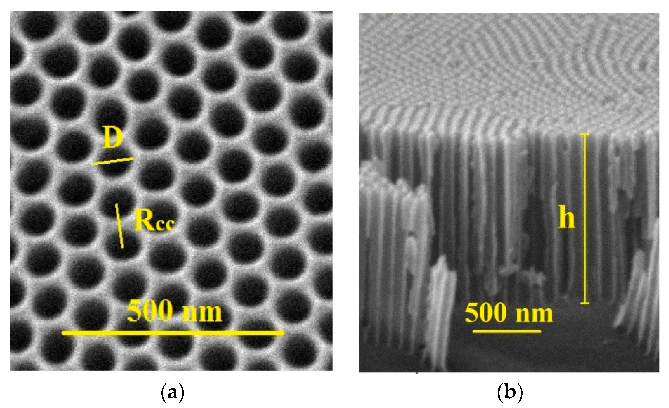
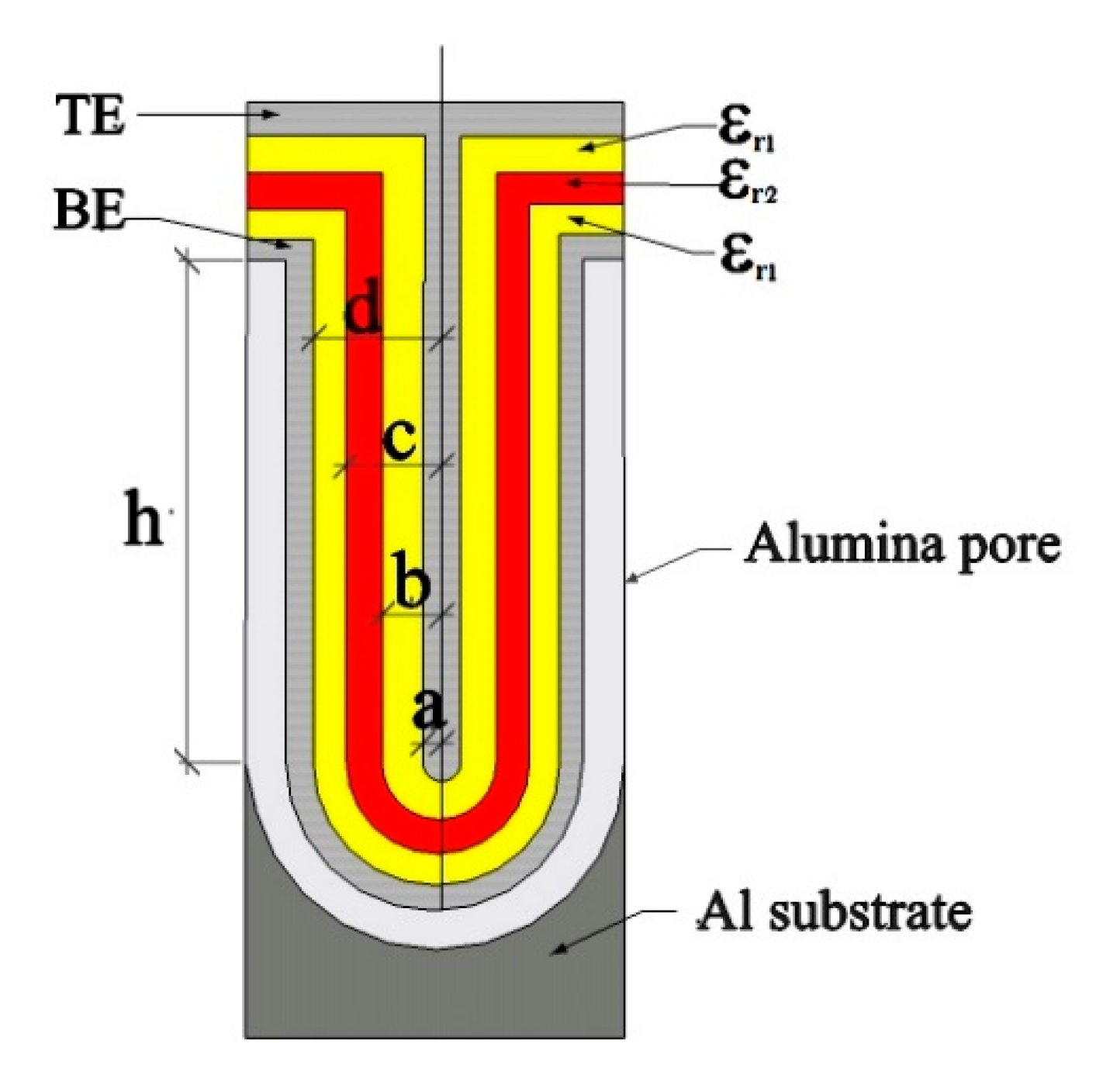
S) of the electrodes. In order to increase the parameter by sizing up the dimensions of the device, NAAMs are used as a substrate, as they offer a high open surface area. By using electrochemical anodization techniques, it is possible to grow hexagonally self-ordered pores whose geometrical parameters can be properly tuned, thus obtaining a highly ordered nanoporous surface with well-defined dimensions, grown on the starting aluminum substrate. The atomic layer deposition (ALD) technique represents an important tool within the nanomaterials additive manufacturing owing to its enhanced possibilities like the fabrication of thin oxide films over micro- or mesoporous surfaces by covering them conformally [11]. The use of the ALD technique allows one to take advantage of the internal surface inside the NAAM’s pores to deposit the three layers that make up the typical structure of the capacitor, that is, the upper and the lower electrode and, between them, the dielectric material. The goal of ALD employment is to reduce the thickness of the dielectric material (d) to the order of nanometers, which results in a consequent increase of capacitance (see Equation (1)). This technique allows one to make coatings of oxide materials over porous substrates, achieving the deposition of layers with thicknesses in the range of nanometers on the internal surface of the nanopores [11,12]. Through ALD performance, it is possible to guarantee a uniform thickness substrate coating [13,14], able to be carried out on porous surfaces with diverse morphologies, whether they are micro-, meso-, or macroporous substrates [15]. Within the storage of energy, ALD is a widespread technique and has a wide range of applications depending on the substrate on which the ALD is made, from the treatment of porous carbon to form a cathodic material that can be implemented with batteries [16], to the coating of ZnO nanowires as electrostatic capacitors [17]. This technique is also used to form supercapacitor devices over multiple substrates. There is a detailed study that applies ALD on NAAMs [4,5,6,7] in a very similar way to what was conducted in this work, developing new electrostatic supercapacitor devices, in which ALD becomes essential in the conformation of its electrodes and dielectric material. However, its range of application goes further, as ALD has been successfully used in recent years for electrochemical capacitor manufacturing over bundles of carbon nanotubes (CNT) [18,19], or TiO2 nanoparticles [20]. One of the main advantages provided by ALD is the performance of electrodes with greater mechanical and chemical stability, owing to the deposition of conformal coatings, which are adapted, in many cases, in the form of nanowires [21,22].
In this work, the manufacturing process of electrostatic supercapacitors by combining the ALD technique and electrochemical anodization of nanoporous anodic alumina templates as starting substrates is reported. The so-formed electrostatic capacitor structure, which consists of a top electrode, a dielectric material, and finally a bottom electrode, has been reduced to nanoscale dimensions by depositing the required materials over patterned nanoporous anodic alumina membranes using the ALD technique. A thin layer of aluminum-doped zinc oxide, 6 nm in thickness, is used as both the top and bottom electrodes’ material, while two different dielectric materials were tested. On the one hand, a triple-layer made by successive combination of a 3 nm in thickness for each layer of silicon dioxide (SiO2), plus titanium dioxide (TiO2), and silicon dioxide (SiO2) again, forming the three-layered SiO2/TiO2/SiO2 dielectric medium, and on the other hand, a single layer with 9 nm in thickness made of alumina (Al2O3).
Regarding the selection of dielectric materials, two criteria have been taken into account. Firstly, the material needs to have a high relative permittivity in order to increase the capacitance. The second criterion is related to the energy gap between its valence and conduction bands, which should be as high as possible, to avoid leakage currents and to reach the maximum working voltage of the capacitor. Among the different insulating materials characterized in the work of [23], the one with the highest relative permittivity (TiO2) and the one with the largest gap (SiO2) are extracted. Unfortunately, these two properties are opposed, with TiO2 being the material with the lowest gap, and SiO2 being the dielectric with the lowest permittivity, as can be seen in Table 1. For this reason, in this work, the combination of these two materials in a triple layer of SiO2/TiO2/SiO2 dielectric is proposed, in such a way that this new material can provide the high performance of permittivity and insulation that TiO2 and SiO2 display by themselves. The electrical behavior of this new multilayered capacitor is compared with the performance of a single layer capacitor, which is conformed by Al2O3 as the dielectric layer. This last dielectric is a material whose ALD deposition has been widely characterized [4,5,6,11,14,24,25], and which also exhibits an intermediate permittivity and band gap values with respect to TiO2 and SiO2.
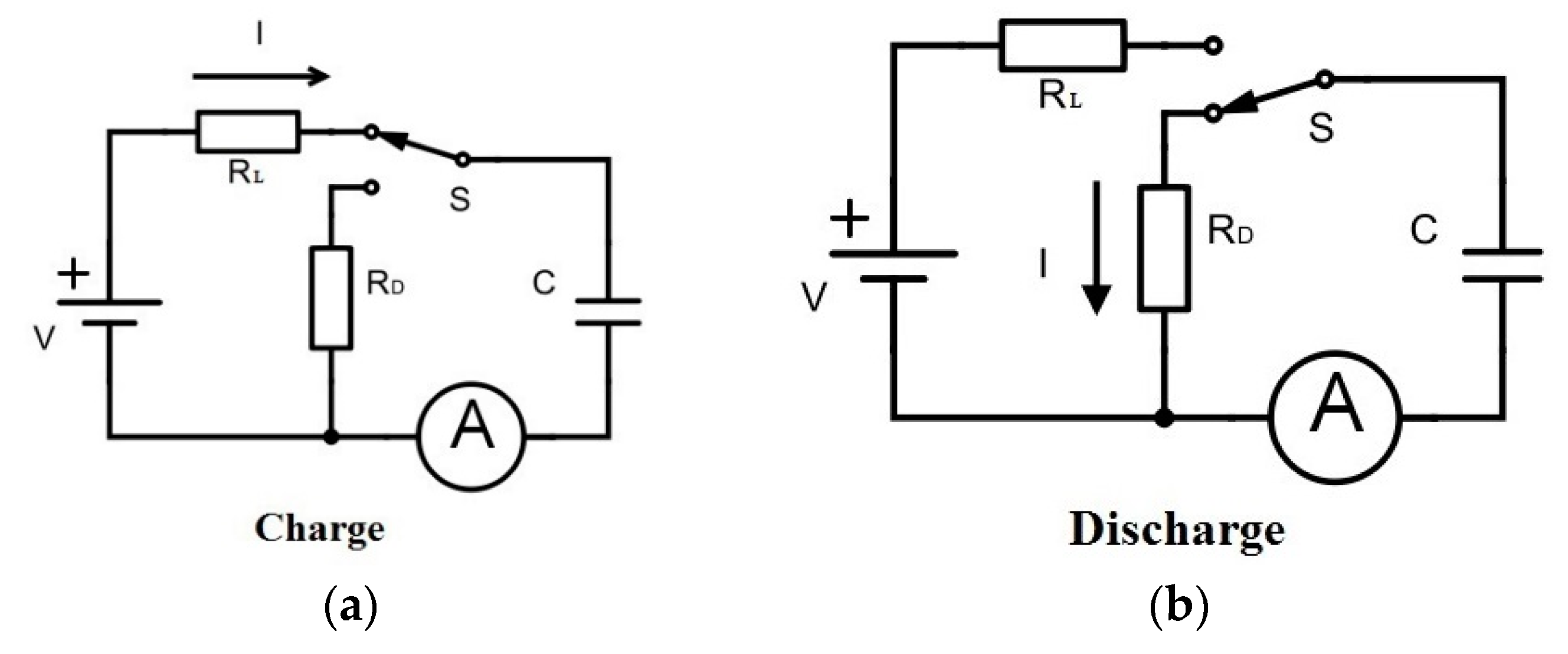
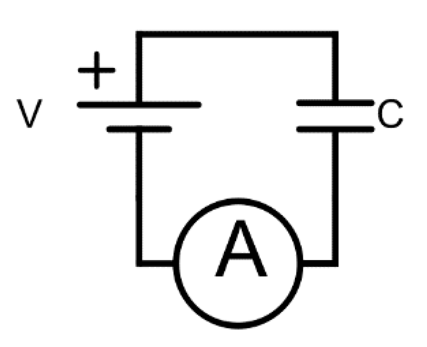
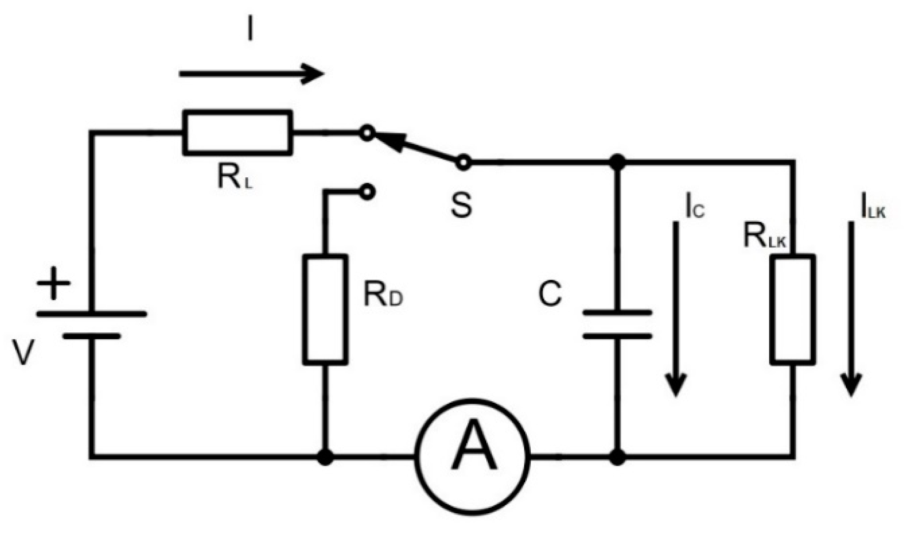
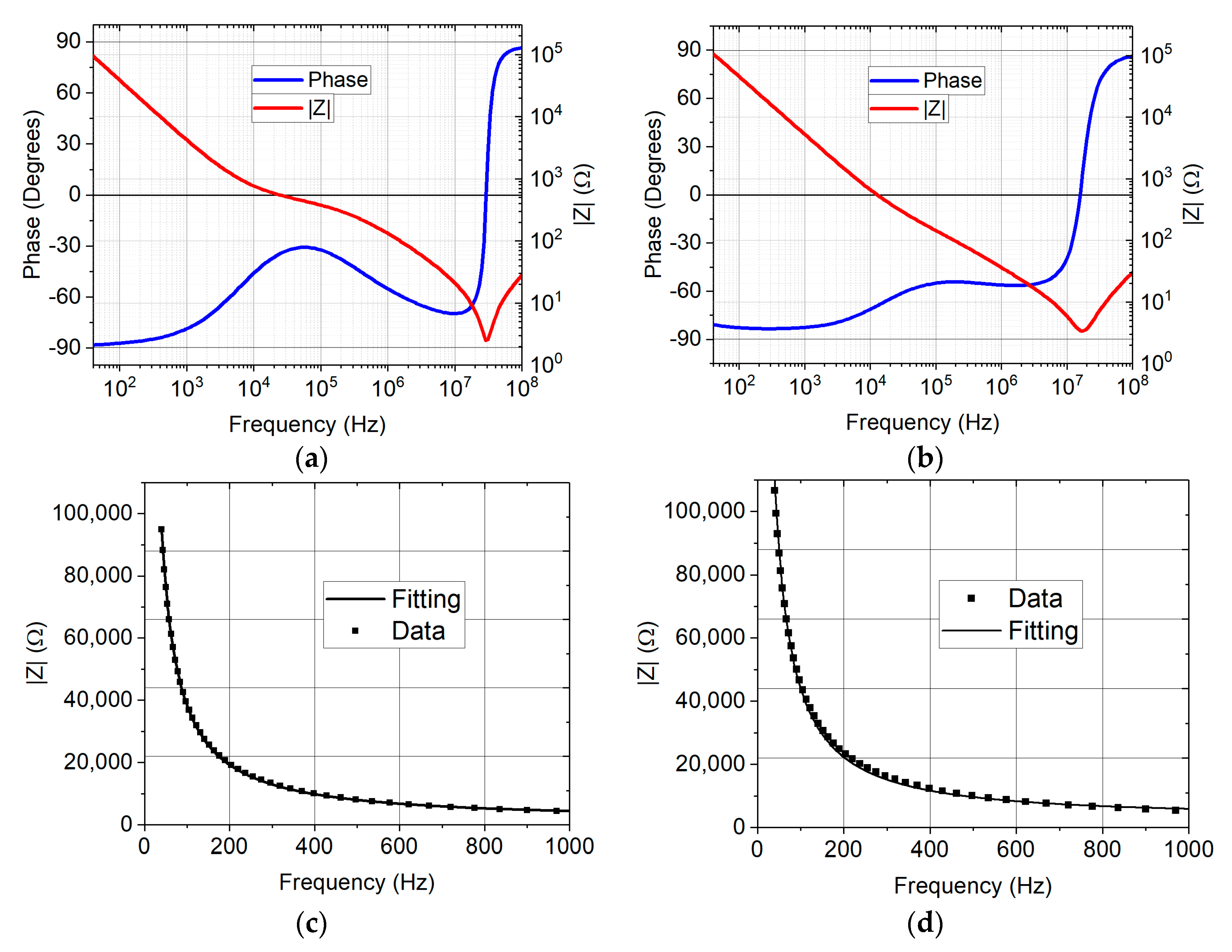
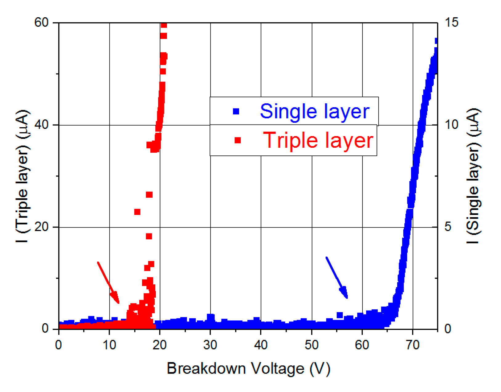
Both oxide materials (Al2O3 and SiO2/TiO2/SiO2) have 9 nm in total thickness and play the role of insulating layers of the capacitors. The electrical properties of these capacitors were tested under different experimental configurations, by measuring characteristic magnitudes such as the impedance and capacitance on the AC and DC frequency regime. In order to give a complete overview on the electrical behavior of these capacitors, breakdown voltage values along with leakage currents are also studied. This demonstrated the ability of using nanostructured materials for designing energy storage supercapacitor devices.

2. Experimental

2.1. NAAMs Manufacturing

NAAMs have been grown on high-purity (99.999%) Al square plates with 2.5 cm sides and 0.5 mm thickness. The pre-anodization treatment consists of immersing the Al plate in an isopropanol bath and then an ethanol bath, both processes applying ultrasound for 5 min. At this point, a series of electrochemical anodization processes begin, using a Keithley 2400 Source-Meter power supply (Tektronix, Inc., Beaverton, OR, USA). Once washed, electropolishing is carried out in an electrochemical cell for 5 min, applying a DC voltage of 20 V and placing the Al plate as the anodic electrode and a Pt mesh as the cathode. A mixture of perchloric acid and ethanol (1:3 vol) at 5 °C is used as electrolyte, which was mechanically stirred during the process.
The growth of the highly ordered porous alumina is carried out through a double process of electrochemical anodization, as reported in the literature [26,27]. The first anodization is carried out in the electrochemical cell by applying a potentiostatic voltage of 40 V between the electrodes, again placing the aluminum plate on the anodic electrode, and a Pt mesh as the cathode, while mechanically stirring throughout. This process takes 24 h and is performed with a 0.3 M oxalic acid electrolyte at 2 °C. Although during this step, a nanoporous alumina membrane has been produced over the aluminum substrate, the pores of which start to become randomly disordered at the sample surface, it is possible to generate the set of honeycomb self-ordered concavities in the Al substrate. In order to access to the Al substrate, the alumina membrane is then removed through selective chemical etching by an aqueous mixture of chromium trioxide and phosphoric acid for 24 h at room temperature. The second anodization is carried out under the same conditions as the first one, but for a time of 45 min, in which the pores already grow in a hexagonally self-orderly manner, by replicating the honeycomb pattern induced in the substrate by first anodization. Two geometrical parameters of the membrane are fixed when applying this procedure, obtaining pores with a height (h) of 1.2 ± 0.1 µm and placed at a horizontal distance between their centers, or interdistance axes (RCC), of 105 ± 5 nm [4] (Figure 1).
After the second anodization, the diameter of the pores is approximately 35 nm, whereby a widening of the pore size is performed by chemical etching after immersing the membrane in a 5% weight phosphoric acid solution at 30 °C for 35 min. The final average pore diameter (D) of 65 ± 3 nm has been obtained [4]. Thus, the pore radius (rp) is around 32.5 nm. Figure 1 displays two scanning electron microscope (SEM, JEOL JSM-5600, JEOL Ltd., Akishima, Tokyo, Japan) images of the NAAMs obtained, showing the morphology and geometrical lattice parameters of the patterned alumina membranes employed in this work.

2.2. ALD Performance

One of the foremost features of thermal ALD is that it is mainly limited to the deposition of oxides, so the deposition of a uniform metallic thin film electrode cannot be easily performed [28]. However, it is possible to achieve a semiconductor oxide material layer performance, capable of constituting the electrode material. Then the use of (1:20) aluminum-doped zinc oxide (AZO) is proposed, because its effectiveness as a semiconductor has already been demonstrated for applications in super-ENCs [29], and its deposition performance by ALD has been widely studied [4,29,30,31].
The ALD process is carried out in a Savannah 100 thermal ALD reactor equipment from Cambridge Nanotech (Waltham, MA, USA), on exposure mode [11], using an Ar flow of 50 sccm as carrier and purge gas. As previously reported [11], a minimum exposure time of 20 s ensures that the precursor gas diffuses properly throughout the substrate, so that the material can be deposited evenly along the entire length of the pores. The number of ALD cycles for each material has been calculated according to the deposition rates shown in Table 2. For example, in the case of the Al2O3 dielectric layer, 80 ALD cycles were performed in order to obtain a layer thickness of around 9 nm. The successive layers of material are deposited on the NAAMs sequentially, beginning with the bottom electrode (BE), then the dielectric material, and ending with the top electrode (TE). The method composed by 20 cycles of diethyl zinc (DEZ) intercalated with 1 cycle of trimethyl aluminum (TMA) [4], is used to achieve ZnO doped with Al atoms. This pulse sequence results in an Al doping level of around 3%, which is the optimum that minimizes the resistivity of AZO layers [29]. Thus, the resulting material (AZO) has semiconductor properties and is used as the electrode material in the conductor/dielectric/conductor (CDC) structure of the capacitors, both in the BE and in the TE with a thickness of 6 nm (see Table 2). As already mentioned in the introduction, capacitors have been manufactured employing two different dielectric materials. On the one hand, a single layer of alumina with total thickness of 9 nm, and on the other hand, the multilayered combination of SiO2/TiO2/SiO2, in which each layer provides a thickness of 3 nm (see Table 2), again making a total thickness of 9 nm. During the deposition of each material, at least two kind of precursors have been used, with the first of them corresponding to the compound containing the metal, and the other H2O, which is responsible of the substrate functionalization. For the deposition of SiO2, it is also necessary to use an O3 precursor, in order to improve the functionalization performed by H2O.
Each precursor used has its own pulse (t1), exposure (t2), and purge (t3) time, as shown in Table 3. Long exposure (t2) and purged (t3) times have been employed, in order to assure that the gaseous precursors have enough time to diffuse into the deep pores.
In order to ensure the successful deposition of the different layers for the C/D/C capacitor structure, SEM images of the membrane surface have been taken after every deposition step. This characterization allows estimating the thickness of the deposited material attending to the reduction in pores diameter after the placement of each one of the layers that form the capacitor, as can be seen in Figure 2a,c,e. From these images, the homogeneity of the deposited layers can also be appreciated. SEM images have been combined with the EDX technique to study the homogeneity of the materials deposited along the entire pore shape, specifically, for the triple dielectric layer capacitor, as shown in Figure 2b,d,f.
As can be seen in Figure 3, the depth profiles for Al (blue trace), Si (red), and Ti (green) remain stable, indicating that a uniform coating along the whole pores size has been carried out.
Using ImageJ software (version 1.52a, National Institutes of Health, Bethesda, MD, USA), the reduction in pore diameter has been calculated from the SEM surface images, and the results are shown in Table 4. Taking into account the starting diameter of 65 nm and the thickness values shown in Table 2, the pore diameter is expected to be around of 53 nm after the deposition of the BE, 35 nm after the dielectric material conformation, and 23 nm after deposition of the TE. The experimental data obtained for the reduction in pore diameter are in good agreement with expectations, so that the respective layers forming the capacitor have the appropriate thicknesses.

2.3. Electrical Contacts

The electrical contacts were made by fixing a copper wire with silver paint directly on the two electrodes of the capacitor. To isolate the electrodes and thus be able to access the bottom one without limitations, part of the NAAM has been masked with a Kapton tape after the BE deposition process. Once the deposition of the dielectric material and the TE is done, the Kapton mask is removed with acetone in such a way that the lower electrode can be further contacted.

2.4. Electrical Characterization

To describe the properties of the capacitors, the electrical behavior of these devices has been analyzed by integrating them on a real electronic circuit. In order to do this, two stages have been differentiated according to the nature of the current supplied to the device. First, the properties have been studied in a dynamic regime, that is, by supplying an alternating current, from 40 Hz to 100 MHz on frequency range. In this work, a precision impedance analyzer model Agilent 4294A (Keysight Technologies, Santa Rosa, CA, USA) has been used. This study allows knowing the characteristic magnitudes of the capacitor, such as the impedance module and phase as a function of the input AC frequency. Secondly, the capacitors were tested in static regime, that is, with continuous input current. This section is essential when checking the energy storage properties of the device because the procedure consists of charging and discharging the device, analyzing the intensity of the current flowing through the capacitor at all times. To allow this, the assembly of a charge–discharge RC circuit is required, as shown in Figure 4.
V represents the DC voltage supplied by the power supply, RL is the load resistance, RD is the discharge resistance, and the values are set as V = 2 V and RL = RD = 2 MΩ. In addition, the circuit is fitted with an ammeter (A) to measure the current intensity (I) flowing through the capacitor branch as well as a switch (S) to select the working mode of the capacitor (C), either charging or discharging. A Keithley 2410 1100 V Source-Meter (Tektronix, Inc., Beaverton, OR, USA) has been used as the power source and a Keithley 2700 1100 V Multimeter/Data Acquisition System (Tektronix, Inc., Beaverton, OR, USA) as the ammeter. Through the data of current intensity transient collected by this device, it is possible to know the energy storage capacity of the capacitor.
By modifying the circuit (see Figure 5), it is possible to find the maximum operating voltage of the device or breakdown voltage, in which the dielectric medium loses its insulating properties and the current circulates through it as if it were a conductive medium, thus losing the properties for energy storage.

3. Mathematical Framework

3.1. Capacitance Estimation

In parallel with the development of the super-ENCs manufacturing procedures, analytical calculations have also been carried out to estimate the electrical properties that can be expected from these devices. Special attention has been paid to magnitudes as the capacitance, the behavior of the phase, and the impedance module when an AC current is applied, as well as the current flowing through the device when in use.
To estimate the capacitance of the device, it is essential to know the symmetry of the substrate on which the layers that make up the super-ENC are deposited. It is considered that inside each one of the NAAM’s pores, a capacitor of cylindrical symmetry is generated, all of them with similar characteristics because of the geometrical uniformity of the NAAM. This single capacitor is connected in parallel with the six single capacitors of cylindrical symmetry present in the six adjacent pores, as a result of the spatial pores distribution with hexagonal symmetry. The total capacitance of the device is then the sum of the capacitance of all the individual capacitors present in the NAAM, as they are connected in parallel with each other. In Figure 6, a diagram of the cross-section of the capacitor generated within a pore can be seen. Three parts can be clearly differentiated according to the geometry, each of them associated with a type of capacitor. In the upper part, a flat symmetry capacitor appears; the intermediate part corresponds to a capacitor of cylindrical symmetry; and the lower part, the bottom of the pore, is associated with a capacitor of hemispherical symmetry. From the calculations reported in the work of [5], where the capacitance provided by each of the parts is calculated, it follows that the main contribution to the total capacitance of the super-ENC comes from the cylindrical part of the pores. Taking into account that the pores of the NAAMs used in this work have a height of 1.2 μm, it is estimated that 95% of the capacitance of the super-ENC comes from the cylindrical part, so the contributions of the top flattened and bottom hemispherical parts are considered negligible.
One of the innovations presented in this work relays on the estimation of the capacitance for triple dielectric layer capacitors (SiO2/TiO2/SiO2) instead of single layer capacitors. This fact constitutes the main contribution of this work with respect to the calculations exposed in previous literature [5], where only single layer capacitors are treated. The capacitance expression for the cylindrical part is then slightly different, as shown in Equation (2), where a, b, c, and d represent the radii of the different dielectric layers with respect to the axis of symmetry of the cylinder. Therefore, the interdistance dc corresponds to the thickness of the internal layer, cb to that of the intermediate layer, and b − a to that of the outer layer of dielectric. Note that a is the distance from the axis of the cylinder to the outer layer of dielectric, a quantity that does not depend on the thickness of the TE. On the other hand, rpd is the thickness related to the BE, but this one does not influence the capacitance calculations. As the internal and external dielectric layers are formed by the same material, two values of relative permittivity come into play, εr1 for the inner and outer layers (SiO2) and εr2 for the intermediate layer (TiO2). In the case of the super-ENC formed by a single layer (Al2O3), the capacitance calculation for a single pore is simpler (Equation (3)), obtaining an expression similar to that shown in the work of [5]. For the single layer capacitor, the thickness and relative permittivity of the dielectric layer is given by da and εr, respectively.
C = 2 π ε 0 h 1 ε r 1 ln ( d b c a ) + 1 ε r 2 ln ( c b )  
C = 2 π ε 0 ε r h ln ( d / a )  
To account for the total capacitance of the super-ENC, the capacitance density is usually calculated, that is, the normalized capacitance per unit area of the NAAM. It is necessary, therefore, to know the number of pores per unit area (σ) that the NAAMs present, which is given by Equation (4), where the hexagonal symmetry of the membranes is also taken into account.
σ = 2 3 R C C 2  
Then, the capacitance density of supercapacitors can be obtained as the result of multiplying Equations (4) and (2) or (3) (for tri-layered or single-layered dielectric material, respectively). By introducing a, b, c, and d distances according to the thicknesses of the respective dielectric layers (see Table 2), the geometrical parameters of the NAAMs, RCC, and h (see Figure 1 in the Manufacturing section), as well as the relative permittivity values, εr, (which are shown in Table 1), it is possible to estimate the capacitance densities for the manufactured super-ENCs (Table 5).
Because manufactured NAAMs have a surface area of 0.7 cm2, the expected capacitances for super-ENCs would be around of 6.7 and 14.8 μF for the triple and single dielectric layer capacitors, respectively.

3.2. Electrical Behavior of the Capacitor in a Real Circuit

Inserting an electronic device in a real circuit is the most appropriate approach to check its operational behavior. In particular, by monitoring the current passing through the capacitor as a function of time, two magnitudes that characterize the device can be known, such as its capacitance (C) and leakage current (ILK). These two features can be measured at the same time with a given experimental configuration, which is the load curve of the capacitor within a DC RC circuit (see Figure 4a). To extract the appropriate information, Equation (5) has been deduced, which represents the decay of the current (I) that the ammeter records as function of time (t), from a maximum current value (I0). As can be seen in Figure 7, and from Equation (5) also, a resistance in parallel to the capacitor has been included in such a way that this element represents the internal resistance of the capacitor itself to the current flow, which is, the leakage resistance (RLK). Note that this resistance is not a real element of the experimental circuit.
Equation (5) shows the intensity flowing through the ammeter as the sum of an intensity that decays due to the capacitance presence (IC), plus the capacitor leakage current, which has a constant value and acts as an offset. This magnitude varies according to the DC voltage (V) applied by the source and the load resistance (RL) of the circuit, as can be seen in Equations (6) and (7). Then, the leakage intensity is a relative property, typical of the circuit or experimental configuration, so this work is also going to account for an intrinsic feature of the capacitor, as it is the leakage resistance. Note also that this model is valid as long as RL is much greater than the internal resistance (R) of the capacitor itself, otherwise R should be taken into account as a series resistor in the capacitor’s branch. The real capacitor could be thus modelled as an RC circuit (where the R value should be the capacitor’s internal resistance and C the capacitance) connected to a resistor in parallel, which represents the leakage resistance. As will be demonstrated below, the internal resistance of the capacitor (R) has a value three orders of magnitude lower than the load resistance (RL), so the presence of the internal capacitor’s resistance can be eliminated in the theoretical charge–discharge circuit (as shown in Figure 7).
I ( t ) = V R L K + R L + I 0 e   R L K + R L R L K R L 1 C t  
I L K = V R L K + R L  
I C ( t ) = I 0 e   R L K + R L R L K R L 1 C t  

4. Results and Discussion

4.1. Dynamic Regime Study

Next, the analysis performed with the manufactured capacitor working under AC conditions will be explained. The data obtained from the impedance analyzer are the impedance module (|Z|) and the capacitor phase as a function of the applied current frequency. As can be seen in Figure 8a,b, both the single layer capacitor as well as the triple layer capacitor show a decay of the impedance module until reaching the resonance frequency, which is located around 2.9 × 10⁷ Hz for the single-layered capacitor, and around 1.7 × 10⁷ Hz for the triple-layered capacitor. Being capacitive electronic components, the output signal of this type of devices has a phase shift of −90° with respect to the input current. However, once the resonance frequency has been exceeded (in which the imaginary part of the impedance is canceled), this value changes to positive 90°, becoming in an inductive element. This pattern can be clearly seen in Figure 8a,b.
| Z | = R 2 + ( 1 2 π υ C ) 2  
Despite that the phase of the manufactured devices does not remain constant at −90° throughout the frequency range analyzed, it remains close to this value within the low frequency range, confirming that manufactured devices behave as capacitors in this region. In fact, this work places special emphasis on the electrical behavior at a low frequency, as its application for electrostatic energy storage requires the use of low frequency input signals. Following this approach, it is considered that, at low frequency, the capacitor can be analyzed as a pure RC circuit. The data of the impedance module as a function of the frequency (υ) have been fitted to Equation (8), in such way that R represents the internal resistance of the device and C its capacitance. Note that all the fittings shown below have been made by least squares, offering a minimum value for R2 of 0.999, while fitting uncertainties have been calculated with a 95% confidence level. In Figure 8c,d, it is possible to see how, between 40 and 1000 Hz, the electrical behavior of the manufactured capacitors are similar to an RC circuit, because fittings exactly represent the experimental data. R and C values have been extracted from the fitting for each type of capacitor, as shown in Table 6.
By considering that R is the internal resistance of the capacitor and taking into account that it reaches values between 2.3 and 3.9 kΩ, they are of in the order of 1000 smaller than the 2 MΩ for the load resistance. In this way, the condition imposed in the mathematical framework section is fulfilled in order to apply Equation (5) to the charge curves.

4.2. Static Regime Study

After an analysis of the capacitor’s properties under an AC input current, another test performed is reported, this time applying an input current DC through the devices. In particular, the charge–discharge cycles have been analyzed on a test circuit (see Figure 4) where the super-ENC prototypes have been placed, obtaining the intensity signal for the capacitor’s branch as a function of time. The typical signal of the charge–discharge cycles in circuits including this type of electrostatic capacitors has two main characteristics; namely, the intensity decays are symmetrical with respect to the time axis, and the curves have different signs. The symmetry is due to the fact that RL and RD have the same value, and the sign differences are caused by the polarity of the capacitor’s branch, which is inverted depending on whether it is in charge mode or in discharge mode. In this work, these conditions are met because RL and RD have a value of 2 MΩ, however, as can be seen in Figure 9, the measured signals have a particularity because the charge cycles appear elevated by a constant value with respect to the 0. This offset is of special interest as it accounts for the leakage current of the capacitor (represented by a red line).
By applying Equation (5) to the load cycle, not only C can be estimated, but also both ILK and RLK can be determined. To improve the quality of the fitting as well as the statistics of the experiment, the signal of three consecutive loads is accumulated in order to fit a curve that contains triple the number of points. As can be seen in Figure 10, the proposed model is fitted to the experimental results, which is shown in Table 7. It should be noted that for the single dielectric layer capacitor, it was not possible to detect the presence of leakage current, being, in the existing case, below 50 nA, which is the minimum resolution of the experiment.

4.3. Breakdown Voltage Test

Finally, the maximum voltage value to which the device can operate was tested. For this, the device is placed in the circuit of Figure 5 and the intensity shown by the ammeter is recorded as a function of the applied voltage. The triple dielectric layer capacitor (SiO2/TiO2/SiO2) exhibited a breakdown voltage of 14 ± 1 V, while the single dielectric layer capacitor (Al2O3) has reached a higher value at 63 ± 1 V. In Figure 11, the voltage ranges at which the capacitors lose their insulating properties and become conductors appear highlighted, as they are indicated by an arrow. It is clear that the multi-layered dielectric SiO2/TiO2/SiO2 is not reaching the insulating features that it was supposed display. On the one hand, it exhibits leakage currents and on the other hand, it has a lower breaking voltage than the Al2O3 capacitor. As no inhomogeneities have been detected in the triple dielectric layer of SiO2/TiO2/SiO2 ALD deposited material, the main causes of this decrease in performance may be other reasons. For example, a higher ALD process temperature for SiO2 causes breaking voltage decreasing [34]. It can also be because of the combination of thin films depositions of different oxides, which may form a new alloyed material that leads to a band-gap reduction with respect to the corresponding ones of SiO2 and TiO2 [35]. In such a way, an a priori insulating material becomes a semiconductor material and, consequently, it could not perform as a dielectric medium.

5. Conclusions

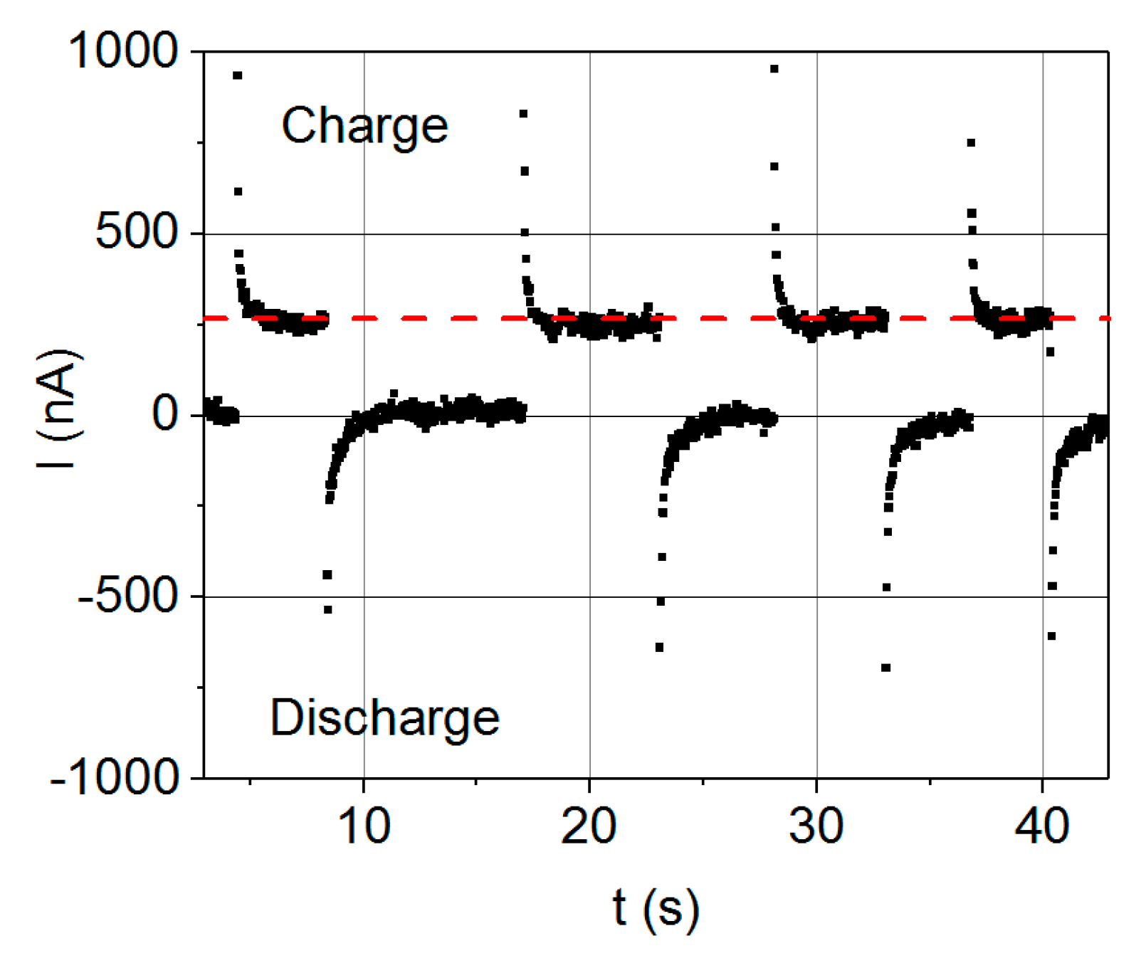
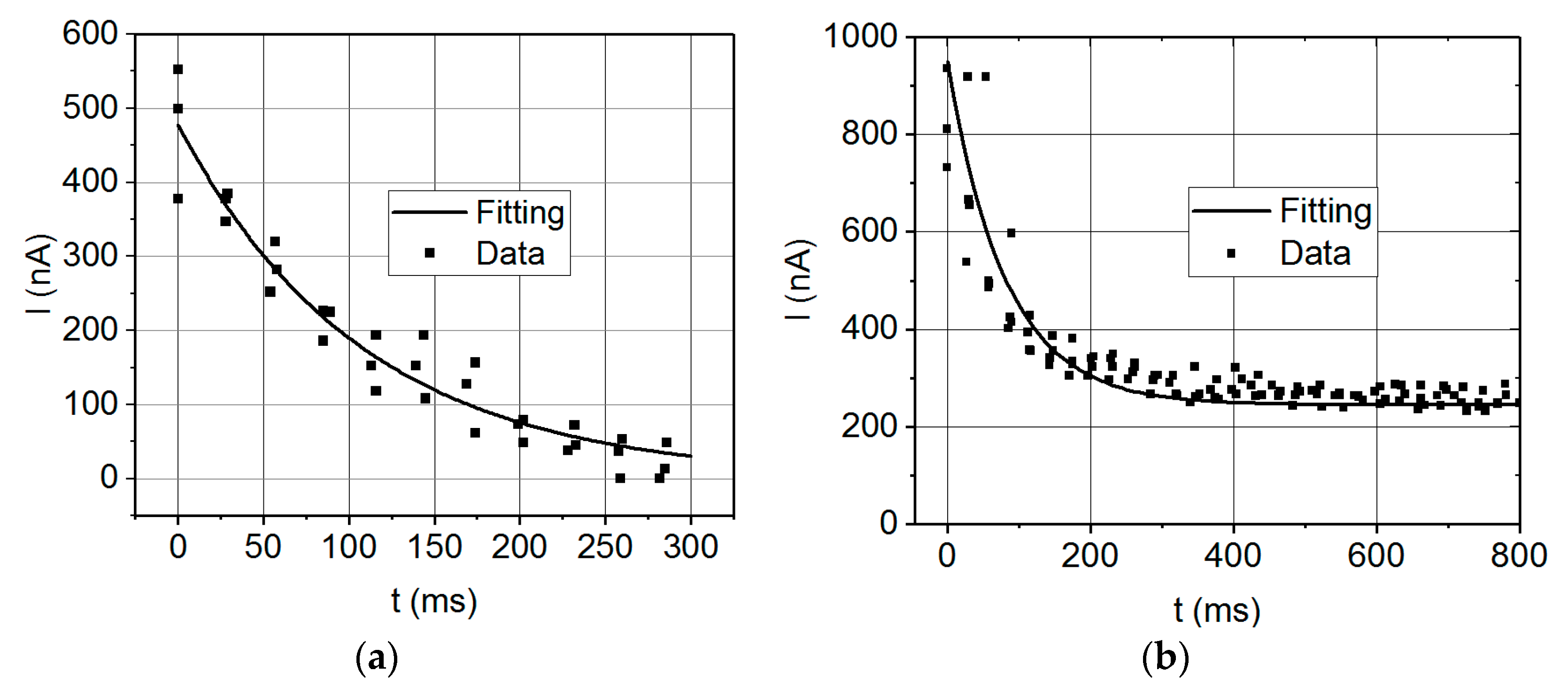
This work has faced the development of electrostatic capacitors and its enhanced possibilities by using nanomaterials, in this way covering the full manufacturing and characterization process of these energy storage devices. An innovative fabrication method has been proposed and achieved, based on the successive combination of an ultrathin layered nanomaterial for the conformation of the dielectric medium of the capacitors. Likewise, an experimental procedure has been followed for the complete characterization of these devices, consisting of three phases, from which the intrinsic magnitudes that completely characterize a capacitor can be measured, such as internal resistance, leakage resistance, capacitance, and breakdown voltage. The test of the manufactured devices in a real circuit, including a model to explain their electrical behavior, which is the main novelty of this study, has obtained experimental results confirming the validity of such a model.
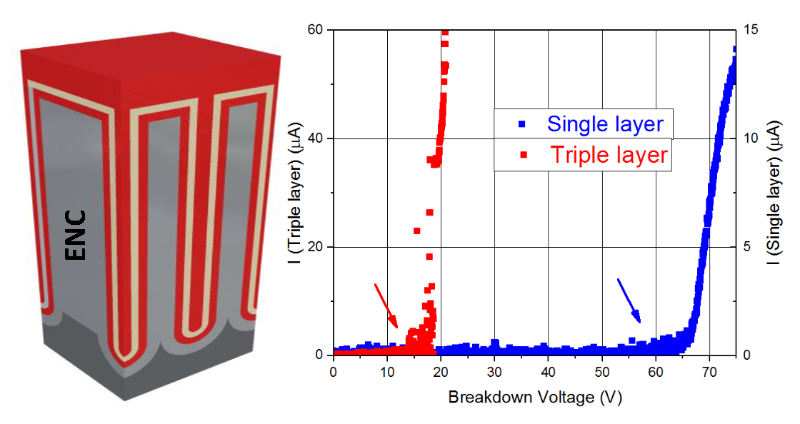
It has been found that the Al2O3 single-dielectric layer capacitors of 9 nm in thickness have been shown to exhibit a better performance than the triple dielectric layer capacitors composed of SiO2/TiO2/SiO2 sheets, each 3 nm in thickness. In particular, single dielectric layer capacitors have less internal resistance (2.3 kΩ), so they are more favorable for storage applications because of a consequent lower power consumption. Al2O3 single-layered capacitors also offer a higher capacitance in dynamic regime (41.6 nF) than those of triple-layered SiO2/TiO2/SiO2. Furthermore, the former display leakage current is lower than 50 nA, so it guarantees that the current losses will be minimal. The main advantage shown by these capacitors is the high value of breakdown voltage (63 V), as a higher working voltage greatly improves the storage capacity of electrical energy of these devices. Only the static regime of capacitance for triple dielectric layer capacitors (93 nF) is higher than that of the single dielectric layer devices (54 nF). However, taking into account all the features in which the Al2O3 capacitors offer better performance, a single property is not enough to affirm that SiO2/TiO2/SiO2 devices have better characteristics.
Nevertheless, the capacitance values derived from our electrostatic supercapacitor prototype are not as high as expected. The values obtained are coherent with the performed analysis, as both the dynamic and the static procedures yield values of the same order of magnitude (nF). However, they are far from the expected capacitance values in the μF range theoretically predicted for these kind of devices, so certain aspects of the manufacture of the supercapacitor devices should be further reconsidered. A feasible explanation on the discrepancies between the expected values of capacities and the experimentally measured ones is that the AZO layer is not properly fulfilling its function as electrode material, for either of two reasons. The first one is that the contact to the AZO layer with silver paint would not be appropriate and thus there is no electron transfer between the AZO layer and the conductive silver paint. The second reason would be that the AZO layer itself is a semiconducting material, and hence it is not able to efficiently conduct the electrical current along the channels of the pores. In addition, the design of the electrical connections of the device becomes critical, because current leakages and short circuits between the electrodes need to be avoided. For example, leakage currents may be decreased in the case of triple layer capacitors, whether or not it can be guaranteed that the electrodes are completely isolated to achieve the most desirable device performance.
There are, therefore, two ways of improving the super-ENCs’ capacitance. On the one hand, the substitution of the AZO layer by using a better conductive material that fits the cylindrical morphology of the pores, such as carbon nanotubes, thus taking advantage of the internal surface of the NAAM to increase the capacitance of the devices. On the other hand, the use of more refined techniques to contact the electrodes, such as wire bonding, would allow precise delimitation of the contact zones, avoiding regions in which short circuits could occur, thus reducing the presence of leakage currents. These advances would significantly improve the performance of the manufactured prototypes that, according to the reported results, could become in very promising energy storage devices. In fact, the super-ENCs are suitable complements for the batteries of electrical systems such as vehicles or electricity supply domestic networks. Besides having a high energy density and faster response under a specific power demand, they also present an environmentally sustainable alternative to the current polluting energy supply systems.

Author Contributions

Conceptualization, A.S.G. and V.M.d.l.P.; Funding Acquisition: V.M.d.l.P. and V.V.; Investigation, L.J.F.-M., A.S.G., and V.V.; Writing—Original Draft Preparation, L.J.F.-M. and A.S.G.; Writing—Review & Editing, A.S.G., V.M.d.l.P., L.J.F.-M., and V.V.; Supervision, V.M.d.l.P.

Funding

This work was funded by the Ministerio de Economía y Competitividad (Spain) under grant MINECO-17-MAT2016-76824-C3-3-R, and IDEPA-ArcelorMittal Proof of Concept grant No RIS3-2015: SV-PA-15-RIS3-2.

Acknowledgments

Funding by Spanish MINECO under grant No MAT2016-76824-C3-3-R is gratefully recognized. The scientific support from the SCTs of the University of Oviedo is acknowledged. Helpful assistance within the electrical measurements provided by the group of Sistemas Electrónicos de Alimentación (SEA) led by J. Sebastián Zuñiga from the University of Oviedo is also gratefully recognized. This work is devoted to the memory of our colleague and friend J. Miguel Mesquita Teixeira.

Conflicts of Interest

The authors declare no conflict of interest.

References

  1. Sakka, M.A.; Gualous, H.; Omar, N.; Mierlo, J.V. Batteries and supercapacitors for electric vehicles. New Gener. Electr. Veh. 2012, 5, 134–160. [Google Scholar] [CrossRef]
  2. Devillers, N.; Jemei, S.; Péra, M.-C.; Bienaimé, D.; Gustin, F. Review of characterization methods for supercapacitor modelling. J. Power Source 2014, 246, 596–608. [Google Scholar] [CrossRef]
  3. Wang, Y.; Guo, J.; Wang, T.; Shao, J.; Wang, D.; Yang, Y.-W. Mesoporous transition metal oxides for supercapacitors. Nanomaterials 2015, 5, 1667–1689. [Google Scholar] [CrossRef] [PubMed]
  4. Iglesias, L.; Vega, V.; Garcia, J.; Hernando, B.; Prida, V.M. Development of electrostatic supercapacitors by atomic layer deposition on nanoporous anodic aluminum oxides for energy harvesting applications. Front. Phys. 2015, 3, 12. [Google Scholar] [CrossRef]
  5. Banerjee, P.; Perez, I.; Henn-Lecordier, L.; Lee, S.B.; Rubloff, G.W. Nanotubular metal-insulator-metal capacitor arrays for energy storage. Nat. Nanotechnol. 2009, 4, 292–296. [Google Scholar] [CrossRef] [PubMed]
  6. Haspert, L.C.; Lee, S.B.; Rubloff, G.W. Nanoengineering strategies for metal-insulator-metal electrostatic nanocapacitors. ACS Nano 2012, 6, 3528–3536. [Google Scholar] [CrossRef] [PubMed]
  7. Pérez, I. Nanoporous AAO: A Platform for Regular Heterogeneus Nanostructures and Energy Storage Devices. Ph.D. Thesis, University of Maryland, College Park, MD, USA, August 2009. [Google Scholar]
  8. Han, F.; Meng, G.; Zhou, F.; Song, L.; Li, X.; Hu, X.; Zhu, X.; Wu, B.; Wei, B. Dielectric capacitors with three-dimensional nanoscale interdigital electrodes for energy storage. Sci. Adv. 2015, 1, e1500605. [Google Scholar] [CrossRef] [PubMed]
  9. Zhao, H.; Liu, L.; Lei, J. A mini review: Functional nanostructuring with perfectly-ordered anodic aluminum oxide template for energy conversion and storage. From Chem. Sci. Eng. 2018, 12, 481–493. [Google Scholar] [CrossRef]
  10. Li, J.; Cheng, X.; Shashurin, A.; Keidar, M. Review of electrochemical capacitors based on carbon nanotubes and graphene. Graphene 2012, 1, 1–13. [Google Scholar] [CrossRef]
  11. Elam, J.W.; Routkevitch, D.; Mardilovich, P.P.; George, S.M. Conformal coating on ultrahigh-aspect-ratio nanopores of anodic alumina by atomic layer deposition. Chem. Mater. 2003, 15, 3507–3517. [Google Scholar] [CrossRef]
  12. George, S.M. Atomic layer deposition: An overview. Chem. Rev. 2010, 110, 111–131. [Google Scholar] [CrossRef] [PubMed]
  13. Yuan, G.; Wang, N.; Huang, S.; Liu, J. A brief overview of atomic layer deposition and etching in the semiconductor processing. In Proceedings of the 17th International Conference on Electronic Packaging Technology, ICEPT 2016, Wuhan, China, 16–19 August 2016; pp. 1365–1368. [Google Scholar]
  14. Vega, V.; Gelde, L.; González, A.S.; Prida, V.M.; Hernando, B.; Benavente, J. Diffusive transport through surface functionalized nanoporous alumina membranes by atomic layer deposition of metal oxides. J. Ind. Eng. Chem. 2017, 52, 66–72. [Google Scholar] [CrossRef]
  15. Daubert, J.S.; Wang, R.; Ovental, J.S.; Barton, H.F.; Rajagopalan, R.; Augustyn, V.; Parsons, G.N. Intrinsic limitations of atomic layer deposition for pseudocapacitive metal oxides in porous electrochemical capacitor electrodes. J. Mater. Chem. A 2017, 5, 13086–13097. [Google Scholar] [CrossRef]
  16. Lei, Y.; Lu, J.; Luo, X.; Wu, T.; Du, P.; Zhang, X.; Ren, Y.; Wen, J.; Miller, D.J.; Miller, J.T.; Sun, Y.-K.; Elam, J.W.; Amine, K. Synthesis of porous carbon supported palladium nanoparticle catalysts by atomic layer deposition: Application for rechargeable lithium–O2 battery. Nano Lett. 2013, 13, 4182–4189. [Google Scholar] [CrossRef] [PubMed]
  17. Wei, L.; Liu, Q.-X.; Zhu, B.; Liu, W.-J.; Ding, S.-J.; Lu, H.-L.; Jiang, A.; Zhang, D.W. Low-cost and high-productivity three-dimensional nanocapacitors based on stand-up ZnO nanowires for energy storage. Nanoscale Res. Lett. 2016, 11, 213. [Google Scholar] [CrossRef] [PubMed]
  18. Fiorentino, G.; Vollebregt, S.; Tichelaar, F.D.; Ishihara, R.; Sarro, P.M. 3D solid-state supercapacitors obtained by ALD coating of high-density carbon nanotubes bundles. In Proceedings of the IEEE International Conference on Micro Electro Mechanical Systems (MEMS), San Francisco, CA, USA, 26–30 January 2014; pp. 342–345. [Google Scholar] [CrossRef]
  19. Kao, E.; Yang, C.; Warren, R.; Kozinda, A.; Lin, L. ALD titanium nitride on vertically aligned carbon nanotube forests for electrochemical Supercapacitors. Sens. Actuators A 2016, 240, 160–166. [Google Scholar] [CrossRef]
  20. Hai, Z.; Karbalaei Akbari, M.; Wei, Z.; Xue, C.; Xu, H.; Hu, J.; Hyde, L.; Zhuiykov, S. TiO2 nanoparticles-functionalized two-dimensional WO3 for high-performance supercapacitors developed by facile two-step ALD process. Mater. Today Commun. 2017, 12, 55–62. [Google Scholar] [CrossRef]
  21. Zheng, W.; Cheng, Q.; Wang, D.; Thompson, C.V. High-performance solid-state on-chip supercapacitors based on Si nanowires coated with ruthenium oxide via atomic layer deposition. J. Power Sour. 2017, 341, 1–10. [Google Scholar] [CrossRef]
  22. Wang, R.; Xia, C.; Wei, N.; Alshareef, H.N. NiCo2O4@TiN core-shell electrodes through conformal atomic layer deposition for all-solid-state supercapacitors. Electrochim. Acta 2016, 196, 611–621. [Google Scholar] [CrossRef]
  23. Robertson, J. High dielectric constant oxides. Eur. Phys. J. Appl. Phys. 2004, 28, 265–291. [Google Scholar] [CrossRef] [Green Version]
  24. Higashi, G.S.; Fleming, C.G. Sequential surface chemical reaction limited growth of high quality Al2O3 dielectrics. Appl. Phys. Lett. 1989, 55, 1963–1965. [Google Scholar] [CrossRef]
  25. Soto, C.; Tysoe, W.T. The reaction pathway for the growth of alumina on high surface area alumina and in ultrahigh vacuum by a reaction between trimethyl aluminum and water. J. Vac. Sci. Technol. A Vac. Surf. Films 1991, 9, 2686–2695. [Google Scholar] [CrossRef]
  26. Masuda, H.; Fukuda, K. Ordered metal nanohole arrays made by a two-step replication of honeycomb structures of anodic alumina. Science 1995, 268, 1466–1468. [Google Scholar] [CrossRef] [PubMed]
  27. Prida, V.M.; Sanz, R.; Vega, V.; Navas, D.; Pirota, K.R.; Asenjo, A. Self-assembled nanoporous oxide membranes. In Encyclopedia Nanosci. Nanotechnol; Nalwa, H.S., Ed.; American Scientific Publishers: Valencia, CA, USA, 2011; Volume 22, pp. 509–532. [Google Scholar]
  28. Geyer, S.M.; Methaapanon, R.; Johnson, R.; Brennan, S.; Toney, M.F.; Clemens, B.; Bent, S. Structural evolution of platinum thin films grown by atomic layer deposition. J. Appl. Phys. 2014, 116, 064905. [Google Scholar] [CrossRef]
  29. Banerjee, P.; Lee, W.-J.; Bae, K.-R.; Lee, S.B.; Rubloff, G.W. Structural, electrical, and optical properties of atomic layer deposition Al-doped ZnO films. J. Appl. Phys. 2010, 108, 043504. [Google Scholar] [CrossRef]
  30. Hou, Q.; Meng, F.; Sun, J. Electrical and optical properties of Al-doped ZnO and ZnAl2O4 films prepared by atomic layer deposition. Nanoscale Res. Lett. 2013, 8, 144. [Google Scholar] [CrossRef] [PubMed]
  31. Elam, J.W.; George, S.M. Growth of ZnO/Al2O3 alloy films using atomic layer deposition techniques. Chem. Mater. 2003, 15, 1020–1028. [Google Scholar] [CrossRef]
  32. Meng, X.; Banis, M.N.; Geng, D.; Li, X.; Zhang, Y.; Li, R.; Abou-Rachid, H.; Sun, X. Controllable atomic layer deposition of one-dimensional nanotubular TiO2. Appl. Surf. Sci. 2013, 266, 132–140. [Google Scholar] [CrossRef]
  33. Bachmann, J.; Zierold, R.; Chong, Y.T.; Hauert, R.; Sturm, C.; Schmidt-Grund, R.; Rheinländer, B.; Grundmann, M.; Gösele, U.; Nielsch, K. A practical, self-catalytic, atomic layer deposition of silicon dioxide. Angew. Chem. Int. Ed. 2008, 47, 6177–6179. [Google Scholar] [CrossRef] [PubMed]
  34. Król, K.; Sochacki, M.; Taube, A.; Kwietniewski, N.; Gierałtowska, S.; Wachnicki, Ł.; Godlewski, M.; Szmidt, J. Influence of atomic layer deposition temperature on the electrical properties of Al/ZrO2/SiO2/4H-SiC metal-oxide semiconductor structures. Phys. Status Solidi A 2018, 215, 1700882. [Google Scholar] [CrossRef]
  35. Uribe-Vargas, H.; Molina-Reyes, J.; Romero-Morán, A.; Ortega, E.; Ponce, A. Gate modeling of metal–insulator–semiconductor devices based on ultra-thin atomic-layer deposited TiO2. J. Mater. Sci. Mater. Electron. 2018, 29, 15761–15769. [Google Scholar] [CrossRef]
Figure 1. (a) Top view of the nanoporous anodic alumina membrane (NAAM) patterned platform supporting the electrostatic nanostructured capacitor (ENC) structure, showing the honeycomb symmetry acquired by the pores. Geometrical parameters are also shown, such as the distance between centers (RCC = 105 ± 5 nm) and the diameter of the pores (D = 65 ± 3 nm). (b) Side view of the NAAM showing the height (h = 1.2 ± 0.1 µm) of the pores as well as their parallel alignment.
Coatings 08 00403 g001
Figure 2. Visualization by scanning electron microscope (SEM) image of the reduction in pores diameter as the layers that make up the capacitor are successively deposited, overlapping one above the other. The left column represents the different stages of the conformation for the single layer capacitor, being (a) the micrograph made after the deposition of the BE; (c) the one taken after the placement of the Al2O3 over the BE; and (e) the one that shows the membrane after the deposition of the BE, the Al2O3, and the TE. Likewise, the column on the right shows the three similar steps for the triple layer capacitor, being (b) the one corresponding to the BE deposition, (d) the one corresponding to the triple layer SiO2/TiO2/SiO2 deposited over the BE, and (f) the one showing the whole BE-SiO2/TiO2/SiO2-TE capacitor structure completely deposited. Note the yellow scale bar of 500 nm for all images.
Coatings 08 00403 g002
Figure 3. SEM image of the cross section for the NAAM with the deposited triple dielectric layer capacitor. On the left side, the substrate of Al can be seen, while on the right side, the NAAM surface appears where the pores are opened. EDX analysis has been carried out along the yellow segment, indicating the presence of different elements through it. The blue line corresponds to Al, while the red and green ones correspond to Si and Ti, respectively.
Coatings 08 00403 g003
Figure 4. Schematic view of the RC charge–discharge circuit. In the charge configuration, (a) the capacitor (C) is powered by the power supply (V) through the load resistance (RL = 2 MΩ). In the discharge configuration, (b) the discharge resistance (RD) is powered by the capacitor. Note that the current (I) flows in different directions through the ammeter (A) depending on whether the configuration is charge or discharge.
Coatings 08 00403 g004
Figure 5. Circuit diagram for breakdown voltage measurements. The power supply (V) is directly connected to the capacitor (C), so the current flowing through the device can be simply monitored by the ammeter (A). A linear increase in the current read by the ammeter indicates the loss of the insulating properties of the capacitor.
Coatings 08 00403 g005
Figure 6. Schematic cross-section of the supercapacitor conductor/dielectric/conductor (C/D/C) structure across a NAAM’s pore. All the sections that make up the device are represented, starting from the aluminum substrate on which the pores are grown. Between the electrodes (TE and BE), the layers forming the dielectric material can be seen, representing those corresponding to the triple layer capacitor in this figure. The yellow color represents the SiO2 layers and the orange represents the one of TiO2, indicating their relative permittivity (εR1 and εR2) and thickness (a, b, c, and d). Note that for the single layered capacitor, instead of three dielectric layers, there would be only one, occupying the same space as the sum of the three layers.
Coatings 08 00403 g006
Figure 7. Theoretical RC charge circuit setup. The ideal model that simulates the electrical behavior of the capacitor (C) in the charging mode has been obtained by adding a parallel resistance, or leakage resistance (RLK), in the capacitor’s branch. The intensity (I) flowing through the load resistance (RL) would be divided into two, the one that circulates through the capacitor itself (IC), and the one circulating through the leak resistance (ILK). Note that this figure is a schema because the real circuit used is the one represented in Figure 4a.
Coatings 08 00403 g007
Figure 8. Module of impedance (|Z|) and phase curves as a function of frequency for the single dielectric layer (a) and triple dielectric layer (b) capacitors. Below, the impedance module data limited to the low-frequency range (from 40 up to 1000 Hz) and its fittings for the single dielectric layer (c) and triple dielectric layer capacitor (d), respectively, are represented.
Coatings 08 00403 g008
Figure 9. Several charge and discharge cycles for the triple dielectric layer capacitor, representing the intensity (I) flowing through the ammeter of the circuit as a function of time (t). An offset current (red dashed line) can be observed for charge cycles, revealing the leakage current of the capacitor.
Coatings 08 00403 g009
Figure 10. Intensity (I) decays in charge cycle for single dielectric layer (a) and triple dielectric layer (b) capacitors as a function of time (t). Its fittings to Equation (5) are also shown.
Coatings 08 00403 g010
Figure 11. Breakdown current–voltage curves for the single dielectric layer (red) and three-layered (blue) capacitors. Representing the intensity (I) recorded by the ammeter (Figure 5) as a function of the applied voltage, it is possible to find the breakdown values, which are indicated by an arrow.
Coatings 08 00403 g011
Table 1. Values of the relative permittivity, εr, and band gap of the different materials employed as dielectric layers for the supercapacitors. The given values are those collected from the work of [23].
Dielectric MaterialεrBand-Gap (eV)
SiO23.99
Al2O398.8
TiO2803.5
Table 2. The different deposited materials are listed, indicating the average deposition rate of each material deposited per atomic layer deposition (ALD) cycle, the chamber temperature during the cycles, the precursor used, as well as the estimated layer thickness for each material. The deposition rates for aluminum-doped zinc oxide (AZO) and alumina have been extracted from the work of [4], while those values for TiO2 and SiO2 are obtained from the works of [32,33], respectively. BE—bottom electrode; TE—top electrode.
MaterialDeposition RateALD Temperature Reaction (°C)PrecursorThickness
AZO0.19 nm/cycle200Diethyl Zinc (DEZ), TMA + H2O6 nm (BE/TE)
Al2O30.13 nm/cycle200Trimethyl Aluminum (TMA) + H2O9 nm
TiO20.07 nm/cycle250Titanium-tetraisopropoxide (TTIP) + H2O3 nm
SiO20.06 nm/cycle180(3-Aminopropyl) trimethoxysilane (APTES) + H2O + O33 nm
Table 3. Timing for ALD processes, with t1 being the precursor pulse time, t2 the exposition time, and t3 the purge lapse. For each material, the exposure times used for each precursor are shown by columns. Note that the precursors and times for Al2O3 are similar, either used for the conformation of AZO or for the Al2O3 dielectric material itself.
Time PeriodZnOAl2O3TiO2SiO2
H2ODEZH2OTMAH2OTTIPH2OO3APTES
t1 (s)0.10.050.10.051110.12
t2 (s)909090906060606060
t3 (s)18018018018012060120120120
Table 4. Average pore diameters after deposition of the different layers, either BE, dielectric, or TE. Data have been obtained from the analysis of scanning electron microscope (SEM) images with ImageJ software.
Deposition StagePore Diameter of Single Dielectric Layer Capacitor (nm)Pore Diameter of Triple Dielectric Layer Capacitor (nm)
BE52 ± 351 ± 5
BE + Dielectric33 ± 438 ± 3
BE + Dielectric + TE27 ± 320 ± 2
Table 5. Distances from the pore axis to the different dielectric layers and estimation of the capacitance density for the manufactured devices.
Dielectric Materiala (nm)b (nm)c (nm)d (nm)Capacitance Density (F/cm2)
Triple layer (SiO2/TiO2/SiO2)17.520.523.526.59.5
Single layer (Al2O3)17.526.521.1
Table 6. Main features obtained from low frequency impedance fitting curves of the manufactured capacitors.
Dielectric MaterialResistance (R)Capacitance (C)
Single layer (Al2O3)2.3 ± 0.2 kΩ41.60 ± 0.07 nF
Triple layer (SiO2/TiO2/SiO2)3.9 ± 0.5 kΩ36.2 ± 0.2 nF
Table 7. Mean results obtained by applying Equation (5) to the charge cycle intensity decays.
Dielectric MaterialLeakage Current (ILK)Leakage Resistance (RLK)Capacitance (C)
Single layer (Al2O3)54 ± 5 nF
Triple layer (SiO2/TiO2/SiO2)220 ± 60 nA7.1 ± 0.8 MΩ93 ± 8 nF

