1. Introduction
By specific surface treatments, diamond surface can form different terminations, such as hydrogen-terminated diamond (H-diamond), oxygen-terminated diamond (O-diamond), fluorine-terminated diamond (F-diamond), and nitrogen-terminated diamond (N-diamond) [
1,
2]. The type of surface termination strongly influences the properties of diamond surface, such as electron affinity, surface conductivity, and work function [
3,
4,
5]. Furthermore, barrier heights for contacts made by metal/diamond are also severely affected by diamond surface terminations. For example, contacts made by metal/H-diamond are likely to show ohmic characteristics or low Schottky barrier heights [
6]. Contacts made by metal/O-diamond and metal/F-diamond usually have relatively high Schottky barrier heights [
7,
8], which will be reduced by annealing for metal/O-diamond contacts [
9]. N-diamond is a quite new type of diamond surface termination [
2]. At present, it seems that few studies have focused on barrier heights for metal/N-diamond interfaces.
Au is a commonly used metal in semiconductor devices. Au/H-diamond contact usually exhibits ohmic characteristics. However, the barrier height of Au/H-diamond contact is difficult to obtain directly by common electrical measurements. Since X-ray photoelectron spectroscopy (XPS) technique can determine the electronic levels directly, it has been used to measure the band offsets for heterojunctions and the barrier height values for metal/semiconductor contacts [
10,
11]. During XPS measurements of barrier height values for metal/semiconductor contacts, the recommended thickness of metal films is about several nanometers, as the electron attenuation length of photoelectrons is only 1–2 nm at XPS energies [
12]. Thus, the barrier height values for Au/H-/O-/F-/N-diamond can be obtained by XPS by depositing ultrathin Au films on diamond surface with different terminations.
Since an ultrathin Au film with a thickness of several nanometers is not a uniform film but consists of islands, it means that the area among metal islands is not covered by metal but exposed to air directly. Thus, barrier height values obtained by XPS measurements may be influenced by conditions of naked diamond area, such as terminations and adsorbates. In particular, XPS results may be seriously affected when the naked diamond area has strong pinning effects. So, it should be an effective method for investigating surface pinning effects by changing surface conditions of naked diamond. Moreover, the size of metal islands and the scale of naked diamond area may also influence XPS measurements. However, it seems that few researches have focused on these points.
In this study, H-/O-/F-/N-diamond have been formed on the same diamond substrate. An Au film with a thickness of 4 nm has been evaporated to form Au/diamond contacts. The barrier height values for Au/H-/O-/F-/N-diamond contacts have been investigated by XPS technique. Then, the thickness of the Au film has been gradually decreased by low-energy Ar+ bombardment until the component of Au almost cannot be detected. The barrier height values for Au/H-/O-/F-/N-diamond contacts have been measured after each Ar+ bombardment. Pinning effects of Au/H-/O-/F-/N-diamond contacts after Ar+ bombardments have been discussed. In the last section, the spatial distribution of the energy band diagram has been calculated by solving Poisson’s equation.
2. Materials and Methods
In this work, 1 ppm boron doped high-temperature high-pressure (HPHT) diamond (100) wafer (3 × 3 × 0.5 mm3) was used as a substrate. The H-diamond was obtained by treating the substrate using hydrogen plasma by microwave plasma chemical vapor deposition. In order to form the H-/O-/F-/N-diamond on one diamond sample, different areas of the H-diamond surface were treated by reactive ion etching (RIE) in O2, CF4, and N2 atmosphere, respectively. The O2 (CF4, N2) flow rate, RIE chamber pressure, radio frequency (RF) power, and etching time were 100 sccm, 10 Pa, 50 W, and 60 s, respectively. An Au film with a thicknesses of 4 nm was deposited by electron beam evaporation on the whole diamond surface.
The 4 nm Au film was gradually treated by low-energy Ar
+ bombardment until the component of Au could not be detected by XPS measurements. The Ar
+ irradiation energy, ion beam current, and spot size were 1000 eV, 2 μA, and 2.5 × 2.5 mm
2, respectively. A commercial X-ray photoelectron spectrometer (ESCALAB 250Xi, Thermo Fisher Scientific Inc., London, UK) was used. The excitation source of the XPS was a monochromatic Al
Kα line with the energy of 1486.6 eV. The vacuum pressure of the chamber was above 1.0 × 10
−7 Pa. The X-ray spot size, analyzer pass energy, and the scanning step were 200 μm, 20 eV, and 0.05 eV, respectively. The binding energies were calibrated by using Au 4
f7/2, Ag 3
d5/2, and the Fermi level of Ag, which are 83.95, 368.21, and 0.00 ± 0.01 eV, respectively [
13]. Peak intensities of all XPS spectra are normalized to unity for the purpose of comparison.
3. Results and Discussion
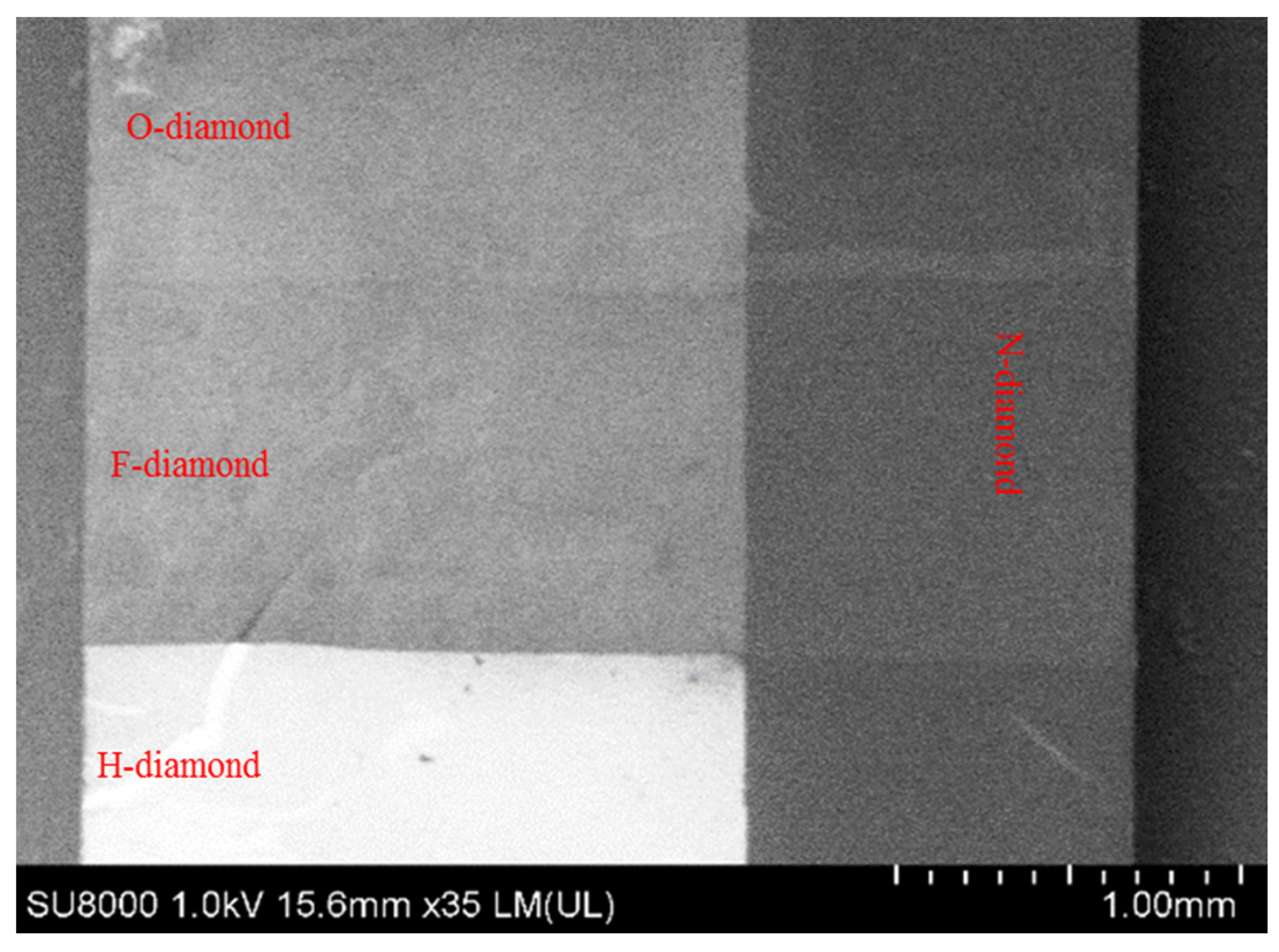
Figure 1 shows the field-emission scanning electron microscopy (FE-SEM) image of the sample just after surface terminations formation. Since the electrical conductivities and surface properties for H-/O-/F-/N-diamond are different, boundary lines can be seen in the image. It can be clearly found that the H-diamond area has the highest brightness, as the H-diamond has p-type surface conductivity. The contrast is due to surface potential differences that influence the secondary electron extraction electrical field at the sample surface. Variations in the surface band bending resulting from a different surface termination induce variation of the surface potential which then generates the contrast observed in
Figure 1.
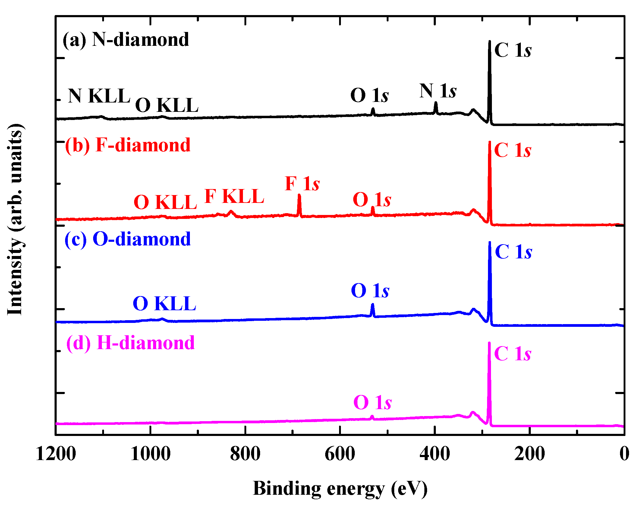
Figure 2 shows the wide XPS spectra of H-/O-/F-/N-diamond. The intensities of O 1
s (around 532 eV) and O KLL (around 984 eV) peaks are obviously higher for the O-diamond, which are on account of O
2 plasma treatment. The nominal oxygen coverage of the O-diamond surface estimated from the O 1
s/C 1
s XPS intensity ratio was about 1.9 monolayer (ML). The extra oxygen should be related to chemisorbed oxygen. The F 1
s (around 685 eV) and F KLL (around 845 eV) peaks are obviously higher for the F-diamond as a result of CF
4 plasma treatment. The nominal fluorine coverage of the F-diamond surface was about 1.6 ML. The extra fluorine should be related to an adsorbed fluorocarbon layer induced by plasma treatment [
14]. The N 1
s (around 402 eV) and N KLL (around 1108 eV) peaks are obviously higher for the N-diamond, as a result of N
2 plasma treatment. The nominal nitrogen coverage of the N-diamond surface was about 0.9 ML. There are O 1
s and O KLL peaks in weak intensities that appeared on the H-diamond, F-diamond and N-diamond, which are attributed to the absorption of impurities in the air.
In the present study, we apply the direct method of XPS to determine barrier heights for Au/H-/O-/F-/N-diamond interfaces. The method is based on the established principle of Kraut’s method, which has also been discussed in the previous report [
15]. All spectra for XPS results obtained from 4 nm Au film areas were shifted by using Au 4
f7/2 spectrum of gold reference sample at the binding energy of 83.95 eV. The barrier height (Ф
BH) values for Au/diamond contacts can be calculated by the following equation,
where, the
values are the C 1
s binding energies for the Au/H-/O-/F-/N-diamond sample, which have been calibrated by using Au 4
f7/2 and Ag 3
d5/2 spectrum as mentioned before. The Δ
Ediamond is the energy separation between the valence band maximum (VBM) and C 1
s for the diamond substrate, which has been obtained by the previous report of 284.01 ± 0.12 eV [
11].
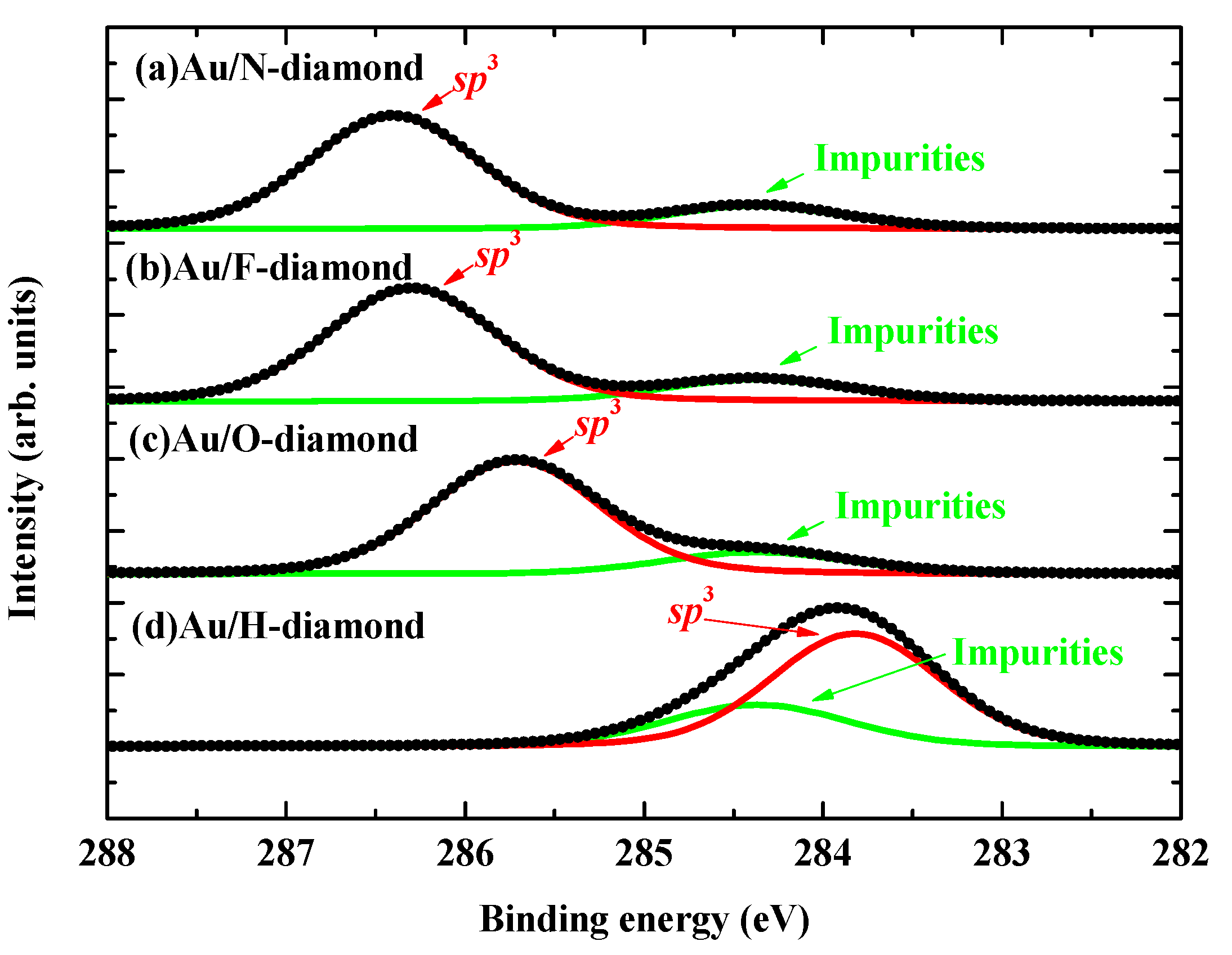
Figure 3 shows the C 1
s spectra obtained from the 4-nm-Au/H-diamond (
Figure 3d), 4-nm-Au/O-diamond (
Figure 3c), 4-nm-Au/F-diamond (
Figure 3b), and 4-nm-Au/N-diamond (
Figure 3a). The backgrounds of all experimental spectra have been corrected with a nonlinear Shirley function. Then, each of the spectra has been fitted with Voigt functions. All peak intensities are normalized to unity for the comparison purpose. The components related to
sp3 C–C bonds are situated at energies of 283.82 ± 0.02 eV for 4-nm-Au/H-diamond, 285.72 ± 0.02 eV for 4-nm-Au/O-diamond, 286.30 ± 0.02 eV for 4-nm-Au/F-diamond, and 286.40 ± 0.02 eV for 4-nm-Au/N-diamond. The components situated at the same binding energy of 284.36 ± 0.02 eV are related to carbon-containing impurities, as metal-island surfaces adsorb carbon containing impurities quite easily. It should be mentioned that the error value of ±0.02 eV is estimated simply from the uncertainty of the graphical determination of the energy position. In other words, the peak position will be obviously incorrect, when we change the peak position by 0.02 eV.
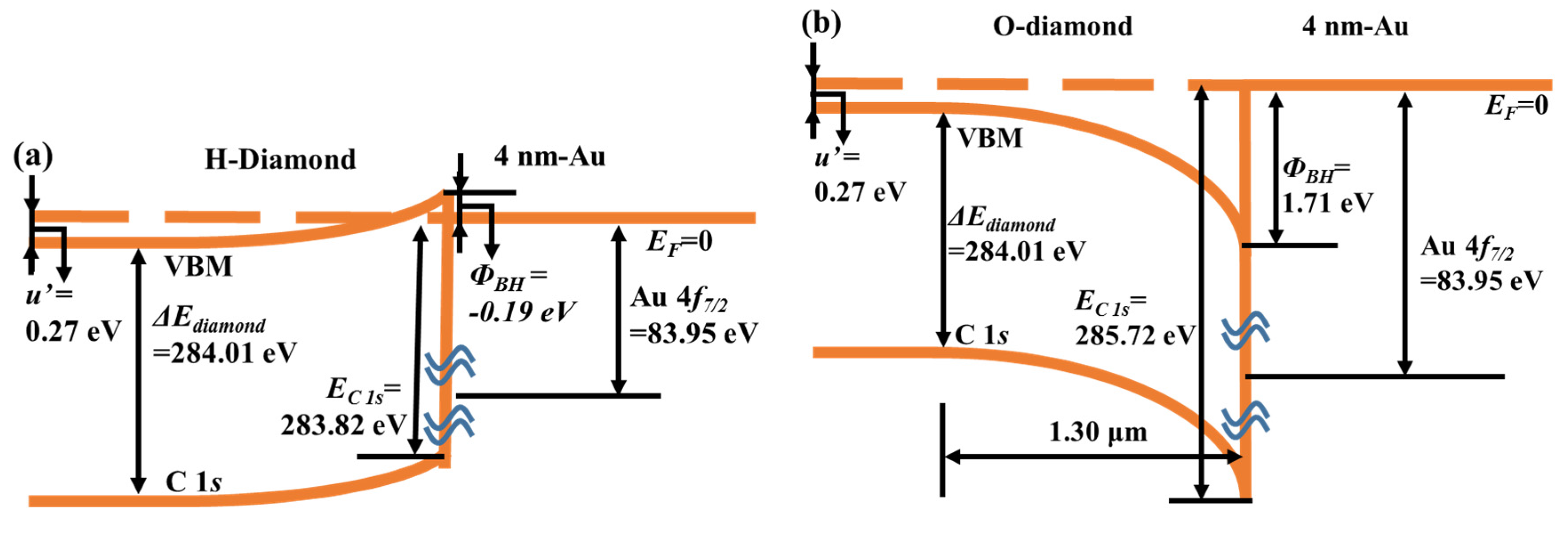
Based on the Equation (1), the Φ
BH values for Au/H-/O-/F-/N-diamond contacts can be calculated to be –0.19 ± 0.14, 1.71 ± 0.14, 2.29 ± 0.14, and 2.39 ± 0.14 eV, respectively. The barrier height of Au/H-diamond is about −0.19 eV, which meets the thermal field emission mechanism with ohmic-contacts [
16]. The barrier heights of Au/O-/F-/N-diamond indicate higher values, illustrating typical Schottky contacts. The barrier height of Au/N-diamond is 2.39 eV, which is a promising structure for Schottky devices.
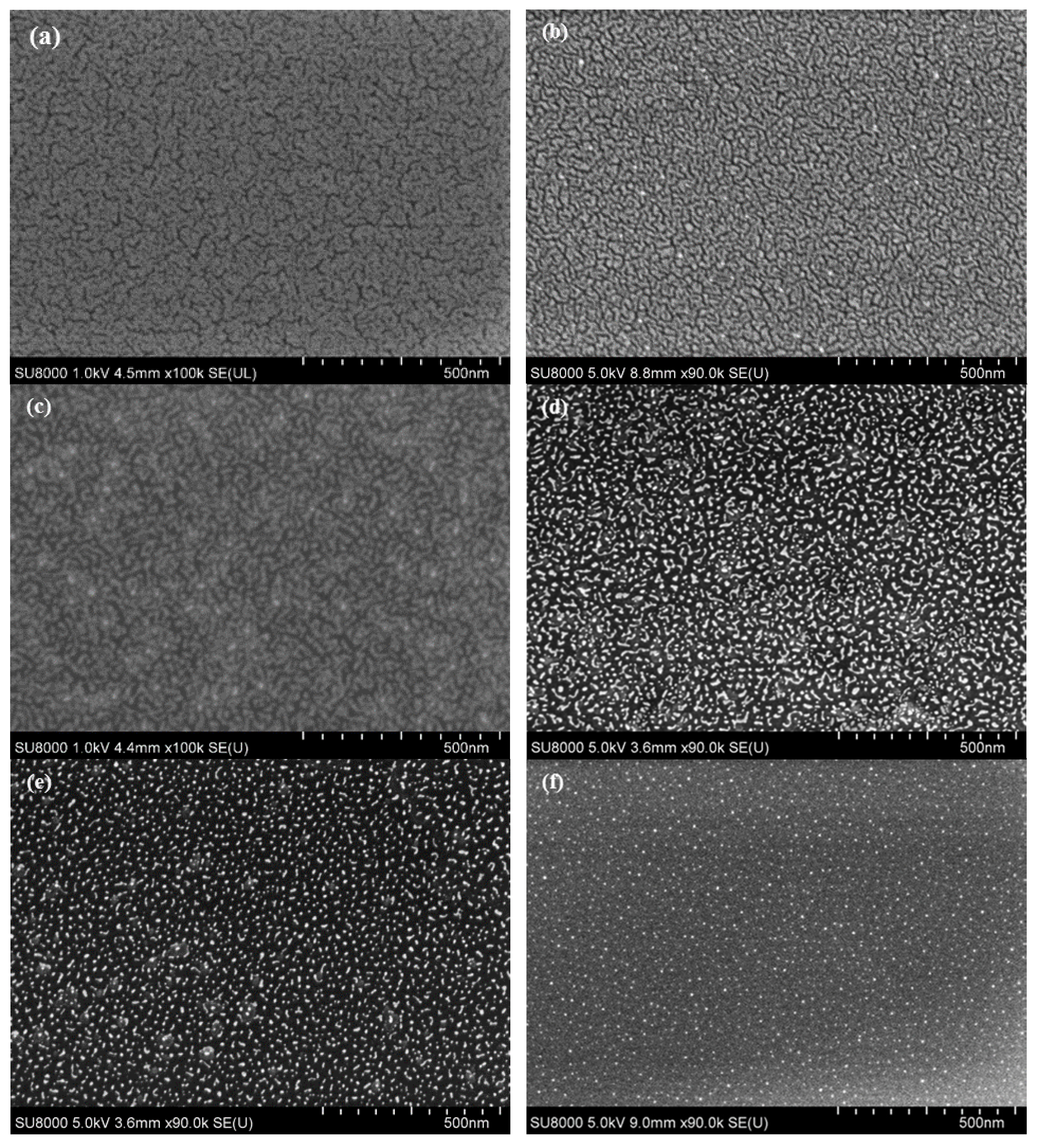
Figure 4a–f show FE-SEM images of the 4 nm Au film bombarded by 1000 eV Ar
+ for 0, 30, 60, 80, 100, and 120 s, respectively. From
Figure 4a, it can be clearly observed that the proportion of exposed diamond surfaces of the 4-nm-Au/diamond is quite small. As Ar
+ bombarding time is extended, Au islands become smaller. When the bombarding time extended to 360 s, Au islands could not be observed any more by FE-SEM (not shown here). After each bombardment, four areas of Au/H-/O-/F-/N-diamond were measured by XPS technique.
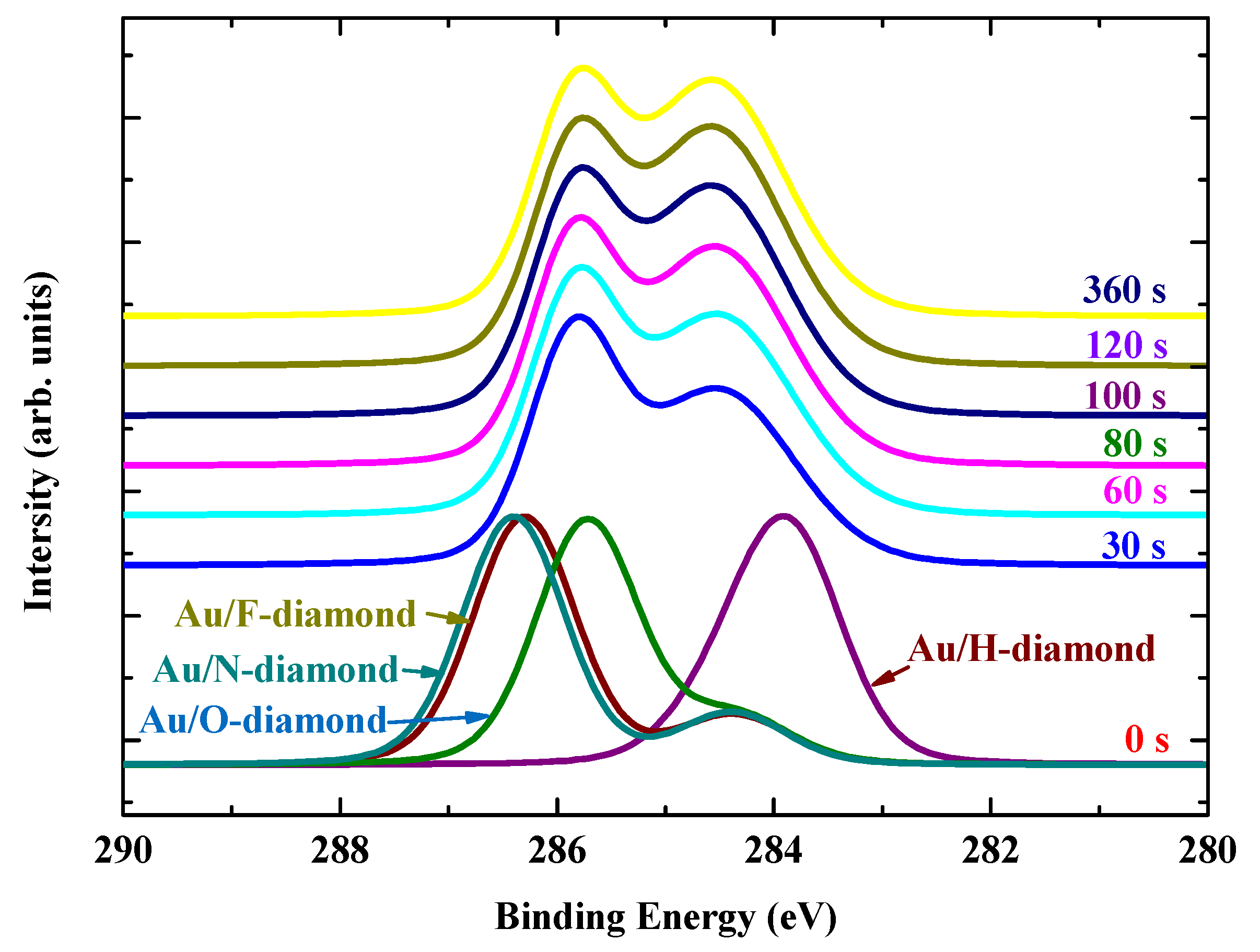
Figure 5 shows the C 1
s spectra obtained from the Au/H-/O-/F-/N-diamond film after bombardments by 1000 eV Ar
+ for 0, 30, 60, 80, 100, 120, and 360 s. It should be mentioned that no obvious difference can be observed for the C 1
s spectra obtained from the Au/H-/O-/F-/N-diamond after the first bombardment for 30 s. In this case, only one C 1
s spectrum has been shown in
Figure 5 after each time of bombardment. The components of each C 1
s spectrum after bombardments are situated at the energies of 284.40 ± 0.02 and 285.84 ± 0.02 eV, respectively. The components at 284.40 eV are attributed to
p-π states, which are related to π bonds between
sp2-hybridized carbon atoms induced by lattice distortions [
17]. It can be observed that the intensity of
p-π states becomes stronger as the bombarding time is extended, which is no longer enhanced after ion bombardment of 120 s as an equilibrium between the induction of defects and the removal of surface atoms.
The components at 285.84 eV are attributed to
sp3 C–C bonds. Based on the Equation (1), the Φ
BH value for the Au/H-/O-/F-/N-diamond after ion bombardments can be calculated to be 1.83 ± 0.14 eV. It is quite interesting that all of the Au/H-/O-/F-/N-diamond have the same Φ
BH value after 30 s bombardment. It is apparent from
Figure 4b that the area of Au islands are still much larger than those of exposed diamond surface after the first bombardment of 30 s. It suggests that the interface structures of Au/H-/O-/F-/N-diamond have been protected. Defects have been only induced to the adjacent diamond area with no metal film coverage. Therefore, it could be thought that barrier heights are no longer affected by the interface structures of Au/H-/O-/F-/N-diamond but the adjacent diamond area with no metal film coverage. As Ar
+ bombarding time extended, Au islands become smaller as shown in
Figure 4, but the binding energy of
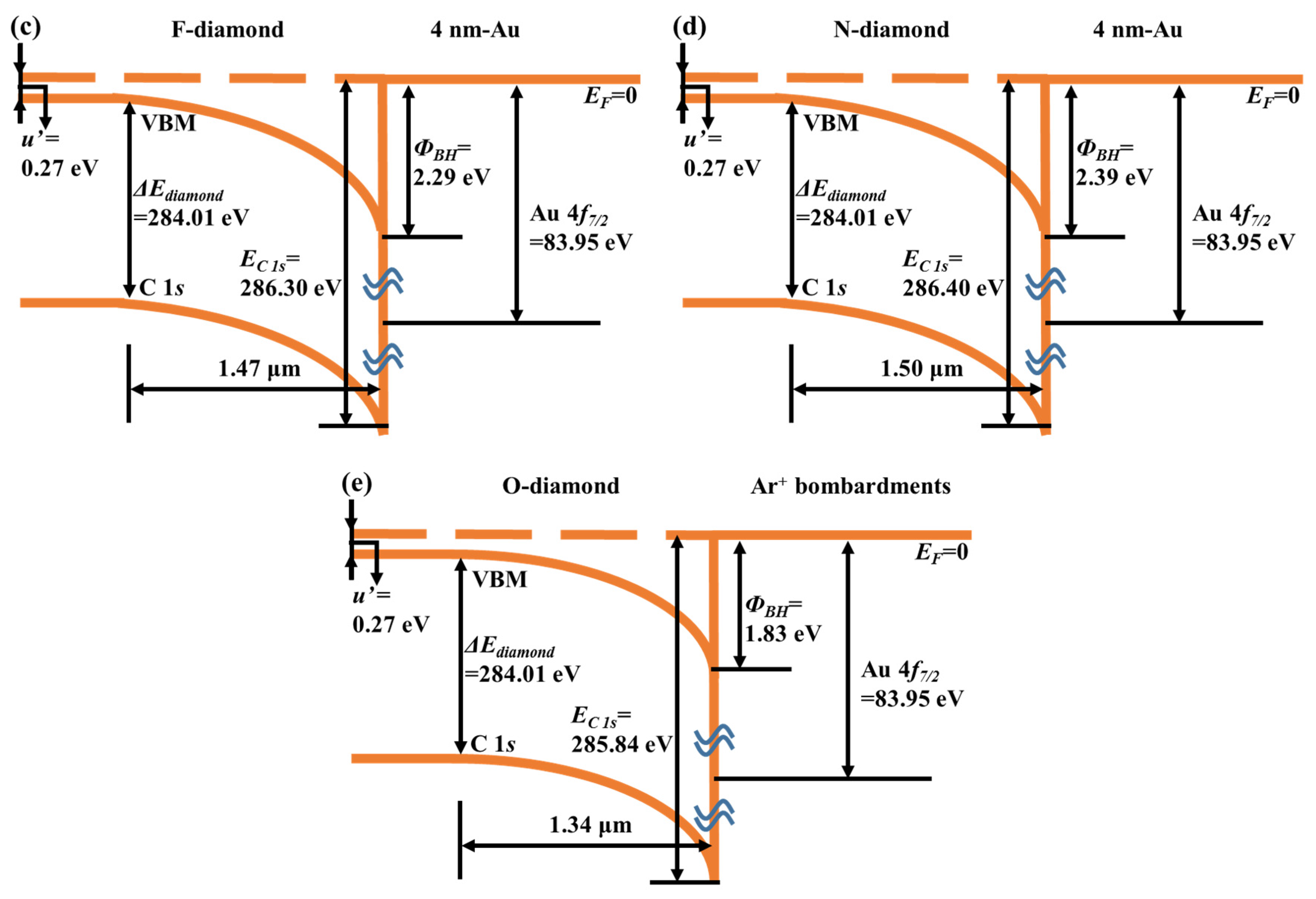
sp3 C–C bonds does not change even after bombardment for 360 s, in this case Au almost cannot be detected by XPS. Thus, barrier heights of Au/H-/O-/F-/N-diamond have been completely pinned to 1.83 eV by the adjacent diamond area with no metal film coverage.
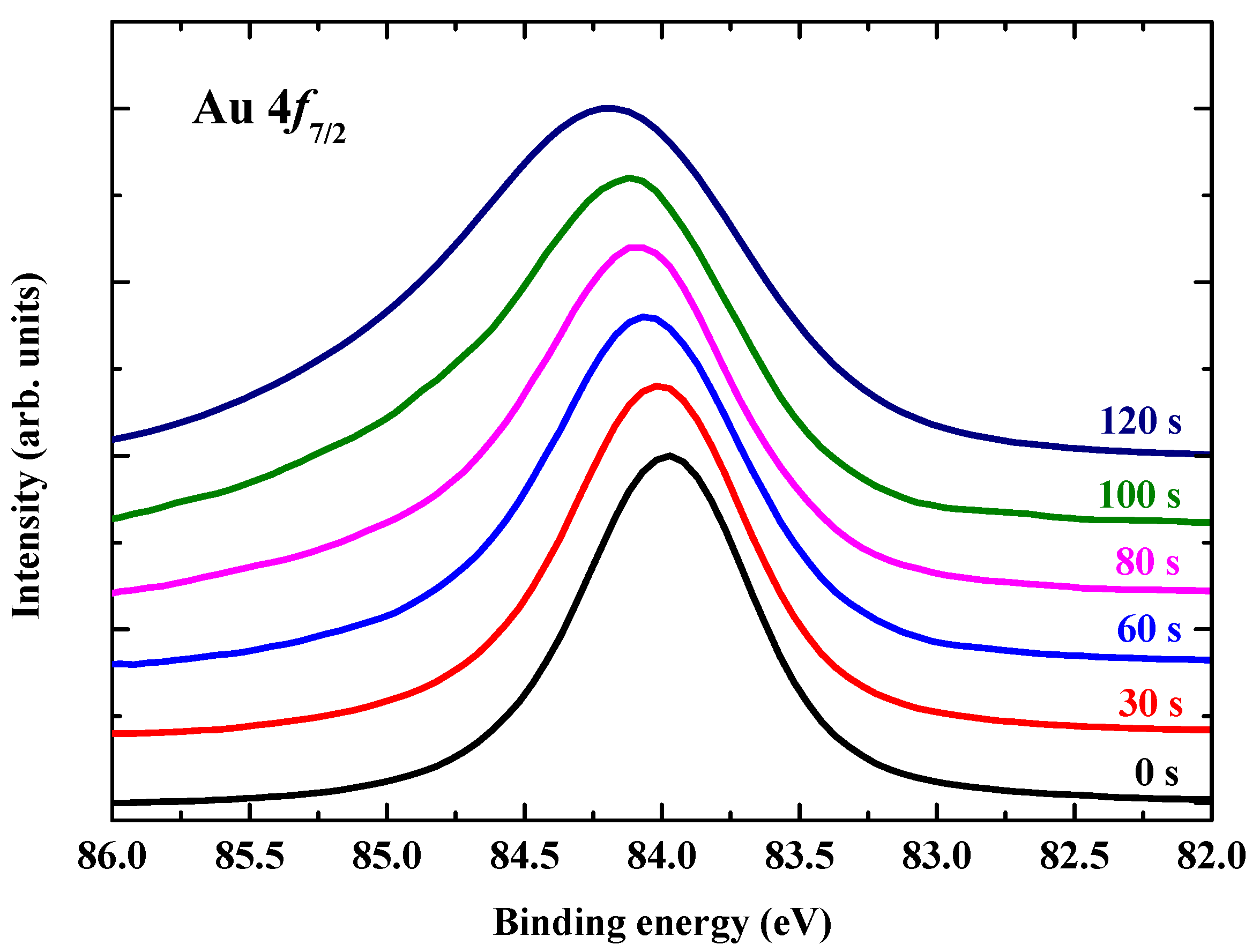
Figure 6 shows Au 4
f7/2 spectra obtained from the Au/H-/O-/F-/N-diamond film after bombardments by 1000 eV Ar
+ for 0, 30, 60, 80, 100, and 120 s. Since no obvious difference can be observed for Au 4
f7/2 spectra obtained from the Au/H-/O-/F-/N-diamond area after bombardments, only one Au 4
f7/2 spectrum has been shown in
Figure 6 after each bombardment. The peak position of Au 4
f7/2 spectrum from 4-nm-Au/diamond film without bombardment is 83.95 ± 0.02 eV, which is gradually shifted to higher binding energies as bombarding time is extended. This is due to the photovoltaic effect in XPS measurement. Broadening of the full-width-at-half-maximum (FWHM) of Au 4
f7/2 has also appeared as the bombarding time is extended. The binding energy for metal will increase when the thickness of metal films decreases to one or two nanometers [
18]. The edge of Au islands is ultra-thin, which will make the binding energy of Au 4
f7/2 higher. For 4 nm Au film without bombardment, the proportion of ultra-thin Au is quite small, so the peak of Au 4
f7/2 is symmetric and its FWHM is quite narrow. As the size of Au islands becomes smaller, the proportion of ultra-thin Au becomes much larger. Thus, the component of high binding energy Au 4
f7/2 increases and the FWHM is broadened.
In order to obtain the energy band diagrams of Au/diamond and diamond with Ar
+ bombarded surface, especially in the spatial sense, it is important to calculate the band bending. Electrostatic potential
V(
x) and space charge density ρ are related via Poisson’s equation,
where ε is the relative dielectric constant of diamond (
ε = 5.8), ε
0 is the vacuum permittivity (ε
0 = 8.85 × 10
−12 F·m
−1), and
x is the coordinate perpendicular to the surface.
u(
x) = −
q ×
V(
x) is the potential energy of an electron in potential
V and that is the quantity that has to be added to all band energies, in particular to
EV and
EC. For convenience, we shall shift the origin of
u(
x) in such a way that the zero of energy corresponds to
EF:
u(
x) ≡
EV(
x) −
EF, where
EF is the Fermi-level and
EV(
x) is the top of the valence band. Thus, Equation (2) can be displaced by the following equation
where
NA− is the density of ionized acceptors with negative electricity. Since the substrate used in this work is 1 ppm boron doped HPHT diamond, the charge in the space charge region mainly consists of ionized acceptors. In addition, we assume that the density of the space charge is independent of spatial distribution in the space charge region. So, the charge density is equal to the density of ionized acceptors. Thus, charge density can be replaced as
. In a nondegenerate semiconductor, the hole concentration
p can be calculated from [
19]
where
ni is the intrinsic carrier concentration,
ND the density of donors,
NA the density of acceptors,
NV the valence band effective density of states,
ga the spin degeneracy factor,
EA the acceptor ionization energy,
k the Boltzmann constant, and
T the absolute temperature.
ND and
ni are negligible in Equation (4) for 1 ppm boron doped HPHT diamond at 300 K. Thus, the hole concentration
p in the bulk can by expressed by
With parameter values of
NA = 1.0 × 10
17 cm
−3,
ga = 4,
NV = 2.35 × 10
19 cm
−3,
EA = 0.36 eV, and
T = 300 K, the hole concentration
p is calculated to be 7.55 × 10
14 cm
−3 by Equation (5). Thus, the charge density of ionized acceptors
NA− in the space charge region is also 7.55 × 10
14 cm
−3. The electric field intensity can be obtained from Equation (3),
where
E is the electric field intensity and
x1 is the boundary of the space charge region. The value of
c1 can be obtained by the boundary condition: when
x =
x1,
E = 0. Thus,
by solving the Equation (6), the electrostatic potential
u(
x) can be expressed as,
the value of
c2 can be obtained by the boundary condition: when
x =
x1,
u =
u′. Thus,
the value of
u′ is the energy separation between the Fermi level and valence band maximum in the bulk of the diamond substrate, which can be obtained by the equation
Thus, the value of
u′ can be calculated as
u′ =
EF −
EV = 0.27 eV. For the structure of Au/O-diamond, the barrier height is 1.71 eV. From the equation of
u(x) ≡
Ev(
x) −
EF, when
x = 0,
u(0) =
EV(0) −
EF = −Φ
BH = −1.71 eV. So, the width of the space charge region can be calculated by Equations (8) and (9) as
x1 = 1.30 μm. By using the same method, the width of the space charge region for Au/F-/N-diamond and diamond with Ar
+ bombarded surface can be calculated as
x2 = 1.47,
x3 = 1.50 and
x4 = 1.34 μm, respectively.
Figure 7 shows schematic band diagrams for the Au/O-/F-/N-diamond interfaces, and diamond with Ar
+ bombarded surface.

