Article

In-Situ Heat Treatment Study on the Nanocrystalline Cr2O3 Film Using an Environmental Scanning Electron Microscope

1
Tianjin Key Laboratory of High Speed Cutting and Precision Manufacturing, Tianjin University of Technology and Education, Tianjin 300222, China
2
Department of Mechanical Engineering, Lund University, Box 118, SE-22100 Lund, Sweden
3
Global Frontier R&D Center for Hybrid Interface Materials, Pusan National University, Busan 609-735, Korea
4
Tianjin Shuangxin Machinery Manufacturing Co., Tianjin 300480, China
*
Authors to whom correspondence should be addressed.
Coatings 2017, 7(12), 225; https://doi.org/10.3390/coatings7120225
Submission received: 9 November 2017 / Revised: 5 December 2017 / Accepted: 7 December 2017 / Published: 8 December 2017
(This article belongs to the Special Issue Hybrid Surface Coatings & Process (Selected Papers from HyMaP 2017))

Abstract

:
In this work, the surface morphology changes of nanocrystalline Cr2O3 film deposited on Si wafer during the heating process were observed in-situ by means of an environmental scanning electron microscope (ESEM). The Cr2O3 film cracked at high temperature due to the cause of thermal stress; the corresponding crack area percentages on the film surface were real-time evaluated using image analysis software (SISC IAS V8.0) based on the principle of gray value analysis. In the meantime, the effects of the heating temperature on the crack area percentage, phase constituents, and grain size of the Cr2O3 film were also studied in detail. The results showed that the percentage of crack area on film surface first increased with the heating temperature rise, and reached the maximum value at around 980 °C, and then gradually declined again. The above trend is closely related to the changes of thermal stress and grain growth in film. In addition, the heat treatment also had a strong influence on the grain size of the Cr2O3 film.

Graphical Abstract

1. Introduction

In the past decades, the field of thin film materials has been developing rapidly, with more new types of films, and improved film quality. Thin film is not only an important asset for daily life services, but also for industrial progress [1]. Chromium oxide thin film is a very interesting research object in the field of thin film application. Because of its low activity in the structure, it is the most stable in all of the homogeneous crystals, so it has very good electrical performance and mechanical properties, which make it applied widely [2,3,4,5]. With the relatively low friction coefficient, high temperature resistance, stable chemical properties and so on, it has been used as a protection material for microelectronic components, and it also has become a barrier material. The Cr2O3 films can also be used in bearings as well as in the combustion cylinder; in addition, such as hard disks and the appearance of digital magnetic recording media need to use this material [6,7,8,9]. As the Cr2O3 films have stable chemical properties, good resistance to environmental corrosion, and have good optical performance, they are also used in fire prevention tools and optical instruments [10,11]. In addition, the Cr2O3 films are also used to absorb solar energy for its higher solar absorbance and lower thermal emittance [12].
The Cr2O3 thin films have been deposited by using various coatings preparing systems [13], such as plasma spraying, electrochemical deposition, arc ion plating, electron beam evaporation, metal–organic chemical vapor deposition, pulsed laser deposition, direct current sputtering, and radio frequency (RF) magnetron sputtering, etc. The AIP (Arc Ion Plating) is the most efficient technology among physical vapor deposition (PVD) techniques for its high ionization efficiency, high ion kinetic energy, and high preparation rate. Ji et al. [14] prepared the Cr2O3 films employing AIP technique, and investigated the influence of oxygen flow rate on the film microstructure, morphology, and mechanical properties. It was found that the macro particles on Cr2O3 film surface decreased gradually with the increase of O2 flux. The most appropriate O2 flux was about 130 sccm, in this experiment, the film possessed the maximum hardness of 36 GPa. Ho et al. [15] had studied Cr2O3/CrN biphasic coatings by cathode arc evaporation technique. The results indicated that the thin Cr2O3 layer could serve as a thermal insulating layer at high temperatures, and to protect the inner coating. Accordingly, the maximum oxidation resistance temperature reached 900 °C in air. Wang et al. [16] had also investigated that Cr2O3 is the only solid chromium oxide that keeps thermodynamically stable at temperatures in excess of 500 °C in the family of CrxOy.
In previous works [17,18,19,20], the effect of substrate bias voltage on film growth mechanism, morphology, microstructure, mechanical properties, tribological properties and thermal stability of the nanocrystalline Cr2O3 films were systematically investigated. Moreover, the double-layered and multilayered CrN/Cr2O3 coatings were also developed. Accordingly the effects of the thickness ratio and the bilayer period on the microstructure, interface, and properties of the above coatings were studied systematically. However, few articles reported the characteristics of Cr2O3 films at high temperatures, as well as the effect of annealing on the film microstructure, phase constituents, and grain size. Especially, how the microstructure and morphology change during the heating process is still unclear. Clarifying these issues is very helpful for the improvement of the Cr2O3 film properties and their practical application.
Therefore, the changes of surface morphology of the AIP Cr2O3 film during heat-treating process were in-situ observed, via an ESEM in a low vacuum atmosphere of 120 Pa, up to a temperature of 1100 °C. Because of the big difference of thermal expansion coefficient between the Si wafer and Cr2O3 films, the big thermal stress was induced in the process of the heat treatment which led to film cracking. The effects of the heating temperature on the crack area percentage of the Cr2O3 film surface were studied in detail. Moreover, the microstructure evolution, particle size, and phase structure of the Cr2O3 film before and after heat treatment were also compared and discussed.

2. Experimental Details

2.1. Preparition of the Cr2O3 Film

The Cr2O3 film was deposited on single-crystalline Si wafer with (100) orientation by using a hybrid coating system. In this work, the only arc ion plating was used. The deposition chamber is a cylindrical shell structure (the diameter of 500 mm, height of 500 mm). The Cr target (99.99 wt % purity) was fixed at a distance of 350 mm from the rotating sample holder that with a diameter of 80 mm connected with arc cathode. The bias supply with a direct current (IDP-1010, KODIVAC Co., Ltd., Seoul, Korea) provided substrate bias voltage. A simulated diagram of the hybrid coating system is presented in Figure 1.
Before the deposition, the substrates were placed in acetone and ultrasonic solution to clean for 20 min, respectively. Next, they were placed on the rack with rotation. The substrate surface is parallel to the target surface and is held at the same level as the target. The samples were heated to 300 °C and then were cleaned by Ar ions bombardment at −800 V negative bias voltages for 5 min, which would remove contaminants and ensure strong adhesive adhesion between the film and substrate. In order to improve the adhesion and to reduce residual stresses, a Cr interlayer with the deposition time of 5 min was introduced. The inert gas (Ar) at a fixed flow ratio was input into the vicinity of Cr target to avoid poisoning during the oxide film deposition process. The purity of Ar and reactive gas (O2) was 99.999%. The Cr2O3 film thickness in this work was about 3.5 μm by adjusting the preparation time. The detailed preparation parameters for nano-crystalline Cr2O3 film fabricated by AIP technique are shown in Table 1.

2.2. Characterizations of the Cr2O3 Film

The surface morphologies of the Cr2O3 film during the heating process were in-situ tested by an environmental scanning electron microscope (ESEM, XL-30, Philips, Amsterdam, The Netherlands). A special hot stage with the circulation of cooling water was mounted in the sample chamber of ESEM for heating sample, which has been introduced in detail in [21]. The film sample was carefully placed in the platinum cup surrounding the thermocouple bead and the alumina and copper lids were placed in position. The heating rate was maintained at about 5 °C/min in the first 20 min and gradually increased to over 15 °C/min later on. The heating temperature ranged from room temperature to 1100 °C which is less than the temperature limit for Si substrate (1300 °C) [22]. And then the sample was cooled down to room temperature at a rate of 20 °C/min. It should be noted that while saving images at low scanning speed, the film microstructure could change before the scan is completed, especially for high heating rates. During the heating process, due to thermal expansion, etc., image drift was very common and at high magnifications this could lead to losing sight of the film being studied. Thus, in order to get an optimized image, and let the visual field in the center of the screen, adjusting the instruments continuously were required. The increase in temperature of the sample invariably led to a loss of contrast in the image, which could be compensated by choosing a higher spot size. All images of surface morphology with a magnification of 1000× were taken at different temperatures and time intervals during the heating process. Each image corresponds to an area of 106 × 80 μm2. Based on the above topography images, the crack area percentage was evaluated using image analysis software (SISC IAS V8.0, SISC, Beijing, China) according to the principle of gray value analysis. The percentage values of crack area were calculated by the crack area on each image divided by the image area.
The transverse-section characteristics of as-deposited and heat-treated Cr2O3 films were obtained using a field emission scanning electron microscope (FE-SEM, Hitachi S-4800, Hitachi, Tokyo, Japan). The phase constituent and microstructure analysis of the Cr2O3 film before and after heat treatment, were conducted using an X-ray diffractometer (XRD, D8 ADVANCE, Bruker, Billerica, MA, USA) with monochromatic Cu Kα (λ = 0.154056 nm) radiation operated at 40 kV and 40 mA. A locked couple θ–2θ mode with a 0.02° step size and a 0.2 s step time was employed. The analyzed range of diffraction angle 2θ was between 30° and 80°.

3. Results and Discussion

3.1. Percentage of Crack Area for the Heat-Treated Cr2O3 Film

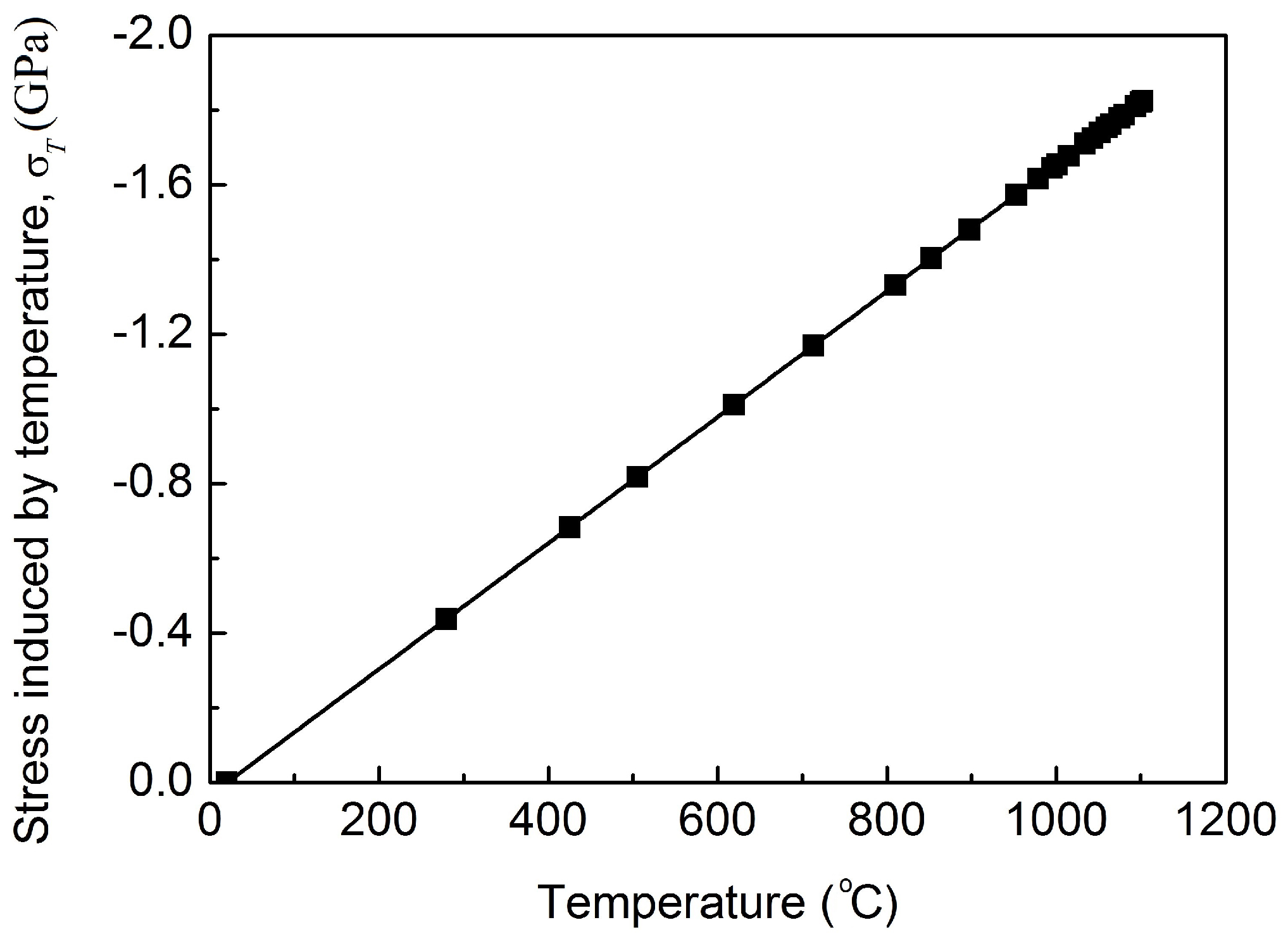
During the heating process, the large thermal stresses were introduced which could cause cracking and spalling of the film. Because the thermal expansion coefficient of the Cr2O3 film (8.7 × 10⁻⁶–9.6 × 10⁻⁶ K−1) and Si wafer (3.5 × 10⁻⁶ K−1) is very different [18], the mismatch of thermal expansion between them becomes more and more obvious which induced large thermal stress. For quantitative analysis, the thermal stress σT in Cr2O3 film induced by temperature rise can be calculated by the following formula:
σ T = Δ α × Δ T × E 1 ν
where ∆α is the difference of thermal expansion coefficient between the Cr2O3 film and Si wafer, ∆T is the difference between heating temperature and room temperature, E and ν are elastic modulus and Poisson’s ratio of the Cr2O3 film, respectively. Here E = 230 GPa and ν = 0.25 were chosen from reference [4], and the thermal expansion coefficient of the Cr2O3 film chose 9.0 × 10⁻⁶ K−1. In this work, the thermal stress induced by temperature is negative which indicates the compressive stress generated, because the thermal expansion coefficient of Cr2O3 film is larger than that of Si wafer.
Figure 2 shows the thermal stress variation in the Cr2O3 film as the temperature rises, which was calculated by Equation (1). It can be seen that the compressive stress increased linearly with the increase of temperature. The maximium stress value was more than −1.8 GPa as the tempeature rose to 1100 °C.
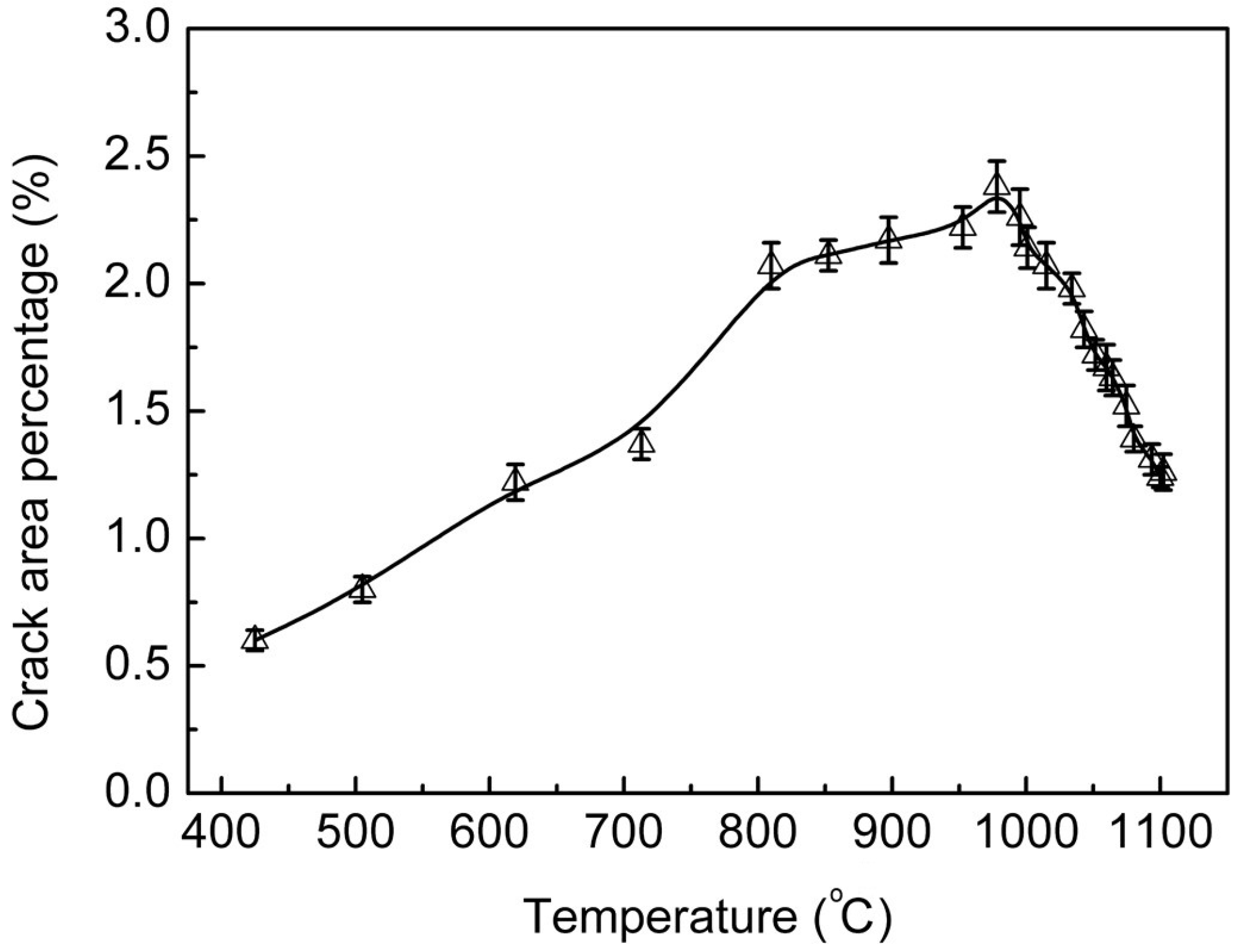
In addition, the crack area percentage on film surface was used to define the variation of Cr2O3 film characteristics during the heating process, and the corresponding results are shown in Figure 3. It can be seen that the crack area percentage of the film first increased gradually with the increase of heating temperature, and reached the maximum value 2.38% at around 980 °C. Since then, it sharply decreased again with the further increase of heating temperature. The thermal stress and grain growth mainly affected the percentage of crack area of the heat-treated film. It is known that usually there are some compressive residual stresses in AIP.
Cr2O3 films [13], with the increase of heating temperature, the Si substrate expanded more than the Cr2O3 film due to the former’s larger thermal expansion coefficient. Thus, the large tensile thermal stresses were introduced into the film according to the principle of thermal expansion and contraction. At first, the compressive stresses in Cr2O3 film can effectively prevent the occurrence and propagation of cracks which derived from thermal stress. The higher the temperature the larger the thermal stresses can be generated. When the thermal stresses reached a certain value the Cr2O3 film started to crack. As the temperature rose further, the increasing thermal expansion difference between the film and substrate favored the propagation and expansion of cracks, which led to a gradual increase in the crack area percentage.
Another factor, the crystal growth can explain why the crack area percentage started to decline sharply as the heating temperature was above 980 °C. It was reported that the crystal growth was closely associated with the temperature and time of heat treatment. By differential scanning calorimetry and thermogravimetric analysis, He et al. [23] also found that the crystallization and vaporization temperatures of the AIP Cr2O3 film are 360 °C and 940 °C, respectively. Their research results further revealed that the grain size of the Cr2O3 film clearly increased after annealing above the crystallization temperature. In this work, the grain growth may be somewhat delayed due to the higher heating rate mentioned above, which brought the very transient grain growth time at different temperatures. The change of temperature would directly affect the grain size and grain boundary sliding, which influenced the mechanical properties of films. In general, the higher temperature incurred the bigger transfer coefficient, grain size, and nucleation rate, but the too high temperature would not be conductive to crystal growth. Moreover, the crystal growth at different directions needed different temperatures to meet surface energy requirement. Usually, the grain boundaries have some certain inhibitory effects on crystal growth. However, there is no restriction to grain growth on both sides of the crack, because they have a free boundary. Thus, these grains would grow toward the crack, which results in a decrease in the crack area percentage of the Cr2O3 film as the temperature exceeded 980 °C. With the further increase of heating temperature, the Cr2O3 grains were growing up and the crack area percentage declined rapidly.

3.2. Surface Morphologies

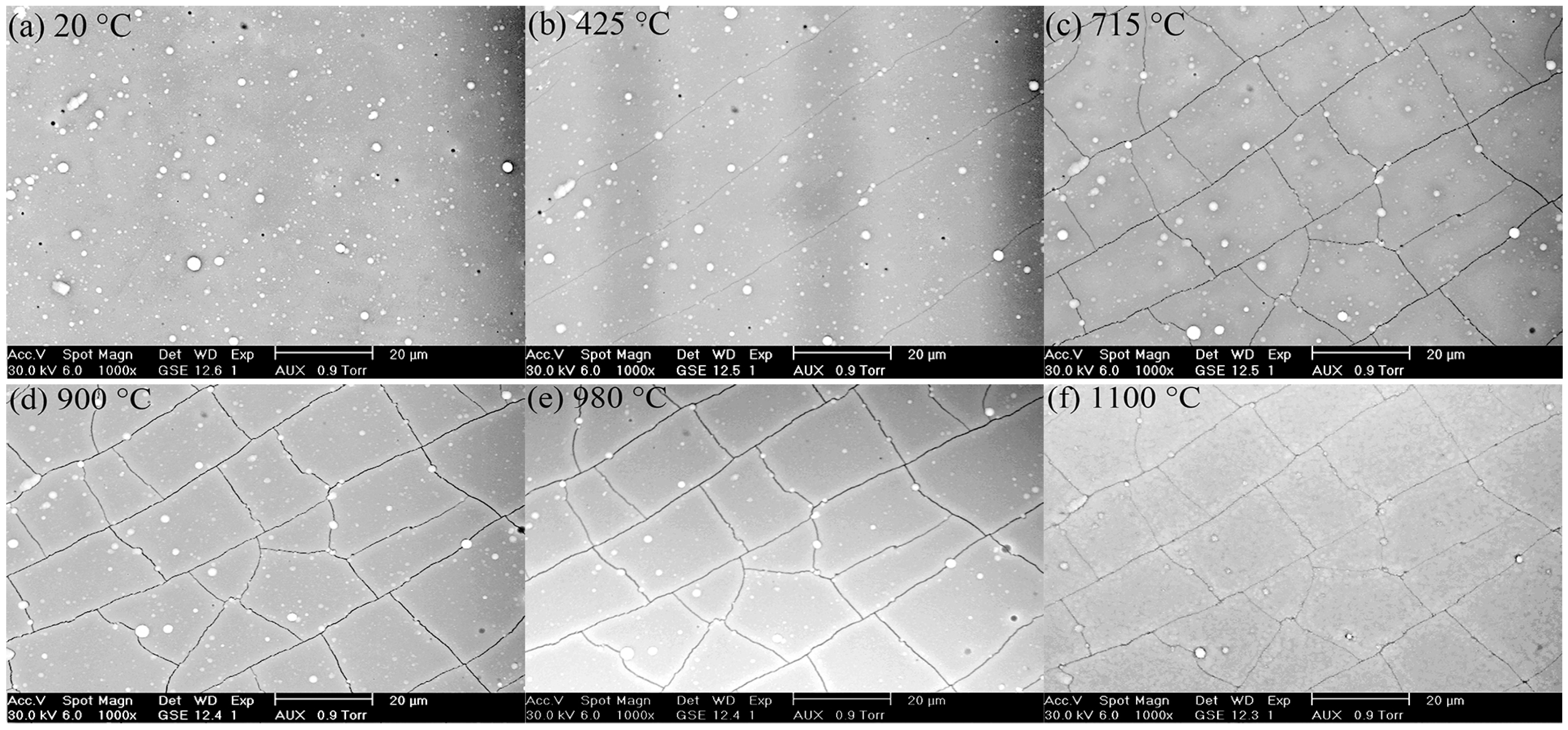
The in-situ surface morphologies of the Cr2O3 film heated at several typical temperatures are shown in Figure 4a–f. From Figure 4a, it can be seen that some macro-particles range from a few hundred nanometers to a few micrometers, and a few hundred or dozens of nanometer pinholes were randomly distributed on the membranes surface at room temperature. The droplets emitted from the arc spots of the Cr target caused macro-particles. It had been reported that there are two kinds of different macroparticles on the AIP Cr2O3 film surface. Some particles that have been deposited previously were embedded in the film, the latest macro-particles fell on the film surface randomly [13]. The growth of the deposited macro-particles was inhomogeneous (which flake from the substrate or shrink during deposition, etching, and heating/cooling in the film chamber), which could lead the pinholes in the films [24,25]. According to these morphology images, the size and amount of macroparticles did not change obviously with the temperature variation.
As the temperature was raised to about 425 °C in Figure 4b, the Cr2O3 film started to crack for the large thermal stresses generated during the heating process. These cracks were parallel to each other and propagated in the same direction. When the tip of crack encountered the macroparticles, it passed around the edge of macroparticles and did not separate them into two parts. That is to say, the initiation and propagation of cracks in the Cr2O3 film may be associated with the macro-particle contamination to a certain extent. Moreover, it was also proved the preferred orientation growth of the Cr2O3 film, which is accordance with the previous XRD study [13]. As the temperature increased to about 715 °C in Figure 4c, some new cracks perpendicular to the original crack direction appeared. There were also a few cracks propagating and extending in other directions. The above cracks were connected together to form a network structure, which effectively released the large thermal stresses. With the heating temperature increased further, the crisscrossing cracks in Figure 4d became wider than before. Namely the crack area percentage was increasing which was attributed to the thermal expansion coefficient of the Si substrate is bigger than the Cr2O3 film, the latter expanded more already mentioned above. At about 980 °C in Figure 4e, the maximum crack gaps could be found, accordingly the crack area percentage reached the maximum. In addition, the tiny drift of visual field and the loss of image contrast can also be observed, which were compensated by continuous adjustments and choosing a bigger spot size. In Figure 4f, the crack gaps reduced significantly. In this case, the heating temperature reached maximum at 1100 °C and the Cr2O3 grains also grew up after a long time heating. The grains on both sides of crack continuously grew toward the gaps, which led to the reduced crack gaps. Kacsich et al. [26] had also reported that the Cr2O3 grain growth was depended on the outward lattice diffusion or grain boundary diffusion, and the inward diffusion of oxygen via grain boundaries.

3.3. Fractured Cross-Section

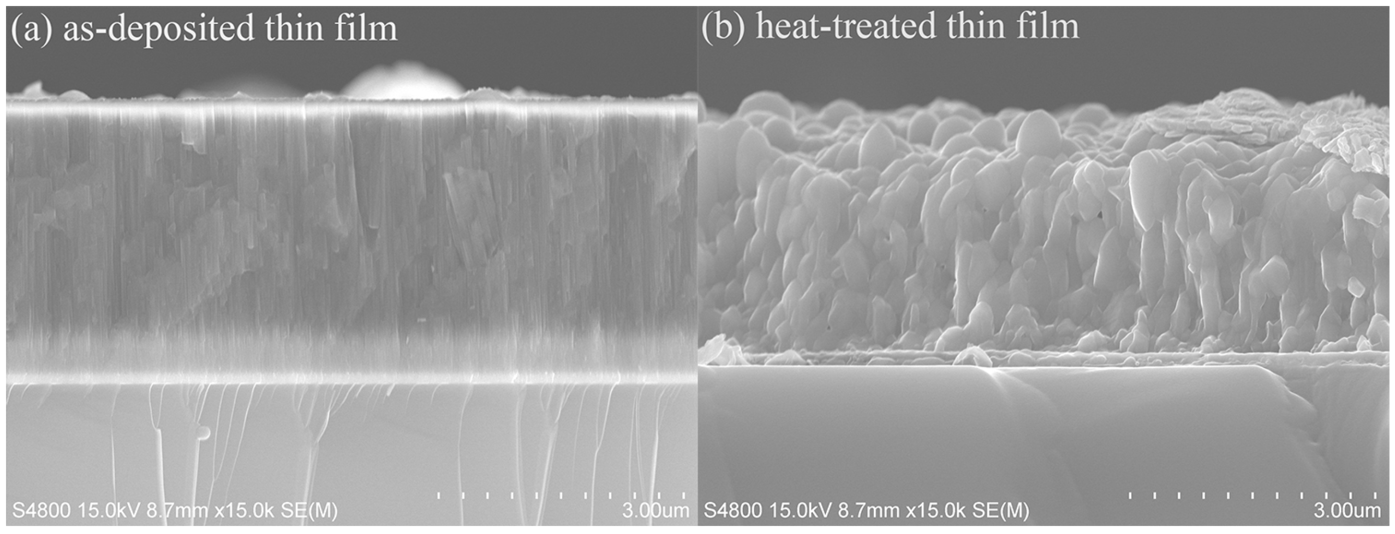
Figure 5a,b depicts the fractured cross-sectional SEM graphs of the as-deposited and heat-treated Cr2O3 thin films. It can be seen clearly that the short and thin Cr2O3 columnar units, Cr interlayer, and Si substrate from Figure 5a, and the film showed a dense microstructure. The AIP Cr2O3 film possesses a nano-scale grain size that the average width of columnar grains is less than 50 nm. The Cr interlayer adhered well to the substrate. There are no pinholes and pores in the columnar structure. However, in Figure 5b, the columnar structure was coarsened significantly after heat treatment. The column width ranged from 200 to 500 nm, and some pores were observed in the film. These pores would seriously affect the film properties, even if its relatively dense microstructure and low defect density. According to previous work [18], the film generated many pores after heat treatment, mainly because the vaporization of Cr2O3 phase at high temperature. Similarly, it had also been reported that the Cr2O3 was the main stable product in the temperature range of 600–950 °C. When the temperature increased further, the Cr2O3 and CrO3 phases coexisted in the system, and the latter would gradually evaporate [27]. In addition, it is also observed that the grains in Cr interlayer have grown up due to high temperature oxidation reaction with residual oxygen in ESEM.

3.4. XRD Analysis

Figure 6 illustrates the X-ray diffraction spectrum of the Cr2O3 film before and after heat treatment. In contrast, the Cr2O3 (202) diffraction peak at the position of 2θ = 44.26° disappeared after heat treatment. The reasons are not clear at present. Additionally, these two spectral lines are very similar, and can be determined as the diffraction peaks of Cr2O3 phase. The four diffraction peaks at the positions of about 2θ = 33.68°, 39.81°, 54.87° and 73.01° corresponded to (104), (006), (116), and (1,0,10) crystal planes of rhombohedral corundum type Cr2O3 were observed, respectively. Moreover, preferred orientation was still (006) crystal plane after heat treating, and the film was only composed of the Cr2O3 phase. There were no other chromium oxide phases detected in the heat-treated film. As a result, the phase constituents of the film after heat treatment did not change except for the reduction of peak intensity, which was attributed to the smaller sample size.
The average grain size Ra of the as-deposited and heat-treated Cr2O3 films were calculated using the full-width at half maximum (FWHM) value of the strongest (006) diffraction peak by the Scherrer’s formula [28], given as:
R a = 0 . 9 λ B cos θ
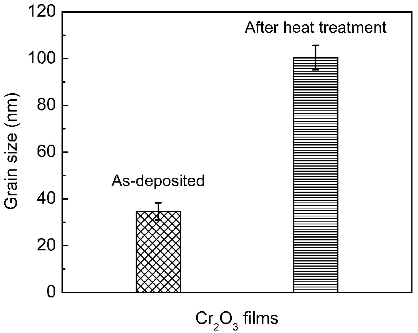
where λ is the wavelength of Cu Kα radiation, B is the calibrated full-width at half maximum of a Bragg peak, and θ is the Bragg angle. Here the diffraction peaks of Si single crystal in θ–2θ mode spectra were used as the calibration reference. Figure 7 shows the average grain size of the as-deposited and heat-treated Cr2O3 films. From the picture that the grain size increased nearly two times from 35 nm to about 100 nm after heat treatment. The fine Cr2O3 grains accelerated the diffusion of grain boundary during the heating process, which resulted in the rapid growth of grains. Here, the interior diffusion of oxygen and external diffusion of chromium promoted the grain growth. Tabbal et al. [29] also obtained similar results, namely at the high temperature, it occurred that a significant improvement in the crystalline quality and a reduction of internal stress. Accordingly, the grain size varied from 50 to 200 nm in the temperature range of 20–950 °C.

4. Conclusions

The crack area percentage was evaluated by the ESEM topography images in-situ observed. With the increase of heating temperature, its value first increased gradually and reached the maximum at about 980 °C, and then sharply decreased again. The thermal stresses and Cr2O3 grain growth explained above phenomenon well.
After heat treatment, the microstructure of the Cr2O3 film was coarsened significantly. The column width ranged from 200 to 500 nm, and some obvious pores were left in the film which was attributed to the vaporization of Cr2O3 phase at high temperature.
The grain size of Cr2O3 film increased nearly two times from 35 nm to about 100 nm after the heat treatment. The high temperature promoted the rapid growth of Cr2O3 grains by the interior diffusion of oxygen and external diffusion of chromium via the grain boundaries.

Acknowledgments

This work was supported by the Global Frontier Program through the Global Frontier Hybrid Interface Materials (GFHIM) of the National Research Foundation of Korea (NRF) funded by the Ministry of Science, ICT & Future Planning (2013M3A6B1078874). In addition, it was also funded by the National Nature Science Foundation of China (51301181), the Tianjin Key Research Program of Application Foundation and Advanced Technology (15JCZDJC39700).

Author Contributions

Tie-Gang Wang and Srinivasan Iyengar performed the experiments; Yanmei Liu and Zubing Yang analyzed the data; Kwang Ho Kim contributed reagents/materials/analysis tools; Tie-Gang Wang and Yu Dong wrote the paper.

Conflicts of Interest

The authors declare no conflict of interest.

References

  1. Singh, B.K.; Mondal, B.; Mandal, N. Machinability evaluation and desirability function optimization of turning parameters for Cr2O3 doped zirconia toughened alumina (Cr–ZTA) cutting insert in high speed machining of steel. Ceram. Int. 2016, 42, 3338–3350. [Google Scholar] [CrossRef]
  2. Gago, R.; Vinnichenko, M.; Hübner, R.; Redondo-Cubero, A. Bonding structure and morphology of chromium oxide films grown by pulsed-DC reactive magnetron sputter deposition. J. Alloys Compd. 2016, 672, 529–535. [Google Scholar] [CrossRef]
  3. Vesel, A.; Mozetic, M.; Balat-Pichelin, M. Reduction of a thin chromium oxide film on Inconel surface upon treatment with hydrogen plasma. Appl. Surf. Sci. 2016, 387, 1140–1146. [Google Scholar] [CrossRef]
  4. Khojier, K.; Savaloni, H.; Ashkabusi, Z.; Dehnavi, N.Z. Structural, mechanical and tribological characterization of chromium oxide thin films prepared by post-annealing of Cr thin films. Appl. Surf. Sci. 2016, 284, 489–496. [Google Scholar] [CrossRef]
  5. Shaukat, S.; Khaleeq-ur-Rahman, M.; Ilyas, U.; Latif, A.; Rawat, R.S. Structural, morphological and optical changes in periodic fractal nanosymmetries of Ni doped chromium oxide ceramic nanostructures. Ceram. Int. 2016, 42, 4952–4963. [Google Scholar] [CrossRef]
  6. Cellard, A.; Garnier, V.; Fantozzi, G.; Baret, G.; Fort, P. Wear resistance of chromium oxide nanostructured coatings. Ceram. Int. 2009, 35, 913–916. [Google Scholar] [CrossRef]
  7. Li, N.-N.; Li, G.-L.; Wang, H.-D.; Kang, J.-J.; Dong, T.-S.; Wang, H.-J. Influence of TiO2 content on the mechanical and tribological properties of Cr2O3-based coating. Mater. Des. 2015, 88, 906–914. [Google Scholar] [CrossRef]
  8. He, N.; Li, H.; Ji, L.; Liu, X.; Zhou, H.; Chen, J. Toughness measurement and toughening mechanisms of arc ion plating Cr2O3 films treated by annealing. Ceram. Int. 2015, 41, 9534–9541. [Google Scholar] [CrossRef]
  9. Garraud, A.; Combette, P.; Giani, A. Thermal stability of Pt/Cr and Pt/Cr2O3 thin-film layers on a SiNx/Si substrate for thermal sensor applications. Thin Solid Films 2013, 540, 256–260. [Google Scholar] [CrossRef]
  10. He, D.; Li, S.; Liu, X.; Zhang, C.; Yu, Q.; Wang, S.; Jiang, L. Preparation of Cr2O3 film by MOCVD as hydrogen permeation barrier. Fusion Eng. Des. 2014, 89, 35–39. [Google Scholar] [CrossRef]
  11. Demirci, E.; Öztürk, M.; Öcal, M.T.; Öztürk, O.; Akdoğan, N. Investigation of spin canting phenomena in perpendicularly exchange biased Pt/Co/Pt/Cr2O3 thin films. Thin Solid Films 2015, 591, 72–75. [Google Scholar] [CrossRef]
  12. Hutchins, M.G. Selective thin film coatings for the conversion of solar radiation. Surf. Coat. Technol. 1983, 20, 301–320. [Google Scholar] [CrossRef]
  13. Wang, T.-G.; Jeong, D.; Liu, Y.; Wang, Q.; Iyengar, S.; Melin, S.; Kim, K.H. Study on nanocrystalline Cr2O3 films deposited by arc ion plating: I. composition, morphology, and microstructure analysis. Surf. Coat. Technol. 2012, 206, 2629–2637. [Google Scholar] [CrossRef]
  14. Ji, A.; Wang, W.; Song, G.; Wang, Q.; Sun, C.; Wen, L. Microstructures and mechanical properties of chromium oxide films by arc ion plating. Mater. Lett. 2004, 58, 1993–1998. [Google Scholar] [CrossRef]
  15. Ho, W.Y.; Huang, D.H.; Huang, L.T.; Hsu, C.H.; Wang, D.Y. Study of characteristics of Cr2O3/CrN duplex coatings for aluminum die casting applications. Surf. Coat. Technol. 2004, 172, 177–178. [Google Scholar] [CrossRef]
  16. Wang, J.; Gupta, A.; Klein, T.M. Plasma enhanced chemical vapor deposition of Cr2O3 thin films using chromium hexacarbonyl (Cr(CO)6) precursor. Thin Solid Films 2008, 516, 7366–7372. [Google Scholar] [CrossRef]
  17. Wang, T.G.; Jeong, D.; Liu, Y.; Wang, Q.; Iyengar, S.; Melin, S.; Kim, K.H. Study on nanocrystalline Cr2O3 films deposited by arc ion plating: II. Mechanical and tribological properties. Surf. Coat. Technol. 2012, 206, 2638–2644. [Google Scholar] [CrossRef]
  18. Wang, T.-G.; Liu, Y.; Sina, H.; Shi, C.; Iyengar, S.; Melin, S.; Kim, K.H. High-temperature thermal stability of nanocrystalline Cr2O3 films deposited on silicon wafers by arc ion plating. Surf. Coat. Technol. 2013, 228, 140–147. [Google Scholar] [CrossRef]
  19. Shi, C.-M.; Wang, T.-G.; Pei, Z.-L.; Gong, J.; Sun, C. Effects of the Thickness ratio of CrN vs. Cr2O3 layer on the properties of double-layered CrN/Cr2O3 coatings deposited by arc ion plating. J. Mater. Sci. Technol. 2014, 30, 473–479. [Google Scholar] [CrossRef]
  20. Shi, C.-M.; Wang, T.-G.; Pei, Z.-L.; Gong, J.; Sun, C. Microstructure, interface, and properties of multilayered CrN/Cr2O3 coatings prepared by arc ion plating. J. Mater. Sci. Technol. 2014, 30, 1193–1201. [Google Scholar] [CrossRef]
  21. Srinivasan, N.S. Dynamic study of changes in structure and morphology during the heating and sintering of iron powder. Powder Technol. 2002, 124, 40–44. [Google Scholar] [CrossRef]
  22. Zeman, P.; Musil, J. Difference in high-temperature oxidation resistance of amorphous Zr–Si–N and W–Si–N films with a high Si content. Appl. Surf. Sci. 2006, 252, 8319–8325. [Google Scholar] [CrossRef]
  23. He, N.; Ji, L.; Liu, X.; Li, H.; Zhou, H.; Chen, J. Role of annealing temperatures on the evolution of microstructure and properties of Cr2O3 films. Appl. Surf. Sci. 2015, 357, 1472–1480. [Google Scholar] [CrossRef]
  24. Ananth, M.P.; Ramesh, R. Sliding wear characteristics of solid lubricant coating on titanium alloy surface modified by laser texturing and ternary hard coatings. Trans. Nonferr. Met. Soc. Chin. 2017, 27, 839–847. [Google Scholar] [CrossRef]
  25. Baloyi, N.M.; Popoola, A.P.I.; Pityana, S.L. Microstructure, hardness and corrosion properties of laser processed Ti6Al4V-based composites. Trans. Nonferr. Met. Soc. Chin. 2015, 25, 2912–2923. [Google Scholar] [CrossRef]
  26. Kacsich, T.; Lieb, K.P. Oxidation of thin CrN and Cr2N films analyzed via nuclear reaction analysis and Rutherford backscattering spectrometry. Thin Solid Films 1994, 245, 4–6. [Google Scholar] [CrossRef]
  27. Panjan, P.; Drnovšek, A.; Kovač, J.; Gselman, P.; Bončina, T.; Paskvale, S.; Čekada, M.; Kek Merl, D.; Panjan, M. Oxidation resistance of CrN/(Cr,V)N hard coatings deposited by DC magnetron sputtering. Thin Solid Films 2015, 591, 323–329. [Google Scholar] [CrossRef]
  28. Obeydavi, A.; Dastafkan, K.; Rahimi, M.; Dezfouli, M.A.G. Insights into post-annealing and silver doping effects on the internal microstructure of ZnO nanoparticles through X-ray diffraction probe. Solid State Sci. 2017, 69, 71–81. [Google Scholar] [CrossRef]
  29. Tabbal, M.; Kahwaji, S.; Christidis, T.C.; Nsouli, B.; Zahraman, K. Pulsed laser deposition of nanostructured dichromium trioxide thin films. Thin Solid Films 2006, 515, 1976–1984. [Google Scholar] [CrossRef]
Figure 1. Sketch map of the hybrid coating system.
Coatings 07 00225 g001
Figure 2. Variation of the thermal stress in the Cr2O3 film with the increase of temperature.
Coatings 07 00225 g002
Figure 3. Variation of the crack area percentage on the Cr2O3 film surface with the increase of temperature.
Coatings 07 00225 g003
Figure 4. In-situ surface morphologies of the Cr2O3 film heated at several typical temperatures: (a) 20 °C; (b) 425 °C; (c) 715 °C; (d) 900 °C; (e) 980 °C; and (f) 1100 °C.
Coatings 07 00225 g004
Figure 5. Fractured cross-sectional SEM images of the Cr2O3 thin film: (a) as-deposited; (b) heat-treated.
Coatings 07 00225 g005
Figure 6. X-ray diffraction spectrum of the Cr2O3 film before and after heat treatment.
Coatings 07 00225 g006
Figure 7. Average grain size of the as-deposited and heat-treated Cr2O3 films.
Coatings 07 00225 g007
Table 1. Detailed deposition parameters for nano-crystalline Cr2O3 film fabricated by arc ion plating technique.
ParametersValue
Base pressure (Pa)3.5 × 10⁻³
Working pressure (Pa)3.0 × 10⁻¹
Deposition temperature (°C)300
Arc current (A)55
DC bias voltage (V)−100
Ar:O2 gas flow ratio (sccm)40:20
Substrate rotation speed (rpm)25
Film thickness (μm)~3.5
Distance between the target and substrate (mm)350