
Article

Optimization of Tin Fluoride Additive Concentration for High-Performance Sn–Pb Perovskite Solar Cells

1
School of Low-Altitude Technology and Electronic Information, Guangdong University of Science and Technology, Dongguan 523668, China
2
Guangdong Provincial Key Laboratory of Sensing Physics and System Integration Applications, School of Physics and Opto-Electronic Engineering, Guangdong University of Technology, Guangzhou 510006, China
*
Author to whom correspondence should be addressed.
Coatings 2026, 16(7), 805; https://doi.org/10.3390/coatings16070805
Submission received: 5 June 2026 / Revised: 29 June 2026 / Accepted: 3 July 2026 / Published: 6 July 2026
(This article belongs to the Special Issue Multilayer Thin Films: Fabrication and Interface Engineering)

Abstract

Tin–lead halide perovskite is a promising narrow-bandgap absorber for high-performance perovskite solar cells. However, the easy oxidation of Sn2+ and the resulting defect formation still limit these films’ quality and photovoltaic performance. Tin fluoride (SnF2) is widely used as an antioxidant additive in Sn-containing perovskites, but its optimal concentration remains strongly dependent on the specific perovskite composition. Herein, we systematically investigate the influence of SnF2 concentration on the film quality and device performance of methylammonium-free Sn–Pb perovskite solar cells. By varying the SnF2 content from 0 to 15% relative to SnI2, we find that an appropriate amount of SnF2 can effectively improve the surface morphology, enhance crystallinity, promote preferred crystal orientation, and suppress defect-assisted non-radiative recombination. In particular, the film with 10% SnF2 exhibits the smoothest surface, with a reduced root-mean-square roughness, enhanced photoluminescence intensity, and a lower trap density compared with the control films. As a result, the optimized device delivers a champion power conversion efficiency of 19.15%, significantly outperforming the control device. This work demonstrates the importance of SnF2 concentration optimization and provides a useful guideline for improving MA-free Sn–Pb perovskite solar cells.

1. Introduction

Mixed tin–lead halide perovskite solar cells (Sn–Pb PSCs) have attracted extensive attention in recent years due to the excellent optoelectronic properties of mixed Sn–Pb perovskites, such as a high absorption coefficient, tunable narrow bandgap, high carrier mobility, and reduced Pb content [1,2,3]. However, the photovoltaic performance of Sn–Pb PSCs is closely related to the chemical stability of Sn2+. To be more specific, Sn2+ can be readily oxidized to Sn4+, which induces Sn vacancies, p-type self-doping, and serious non-radiative recombination [4,5]. Therefore, it is vital to suppress Sn2+ oxidation and regulate the crystallization process to form high-quality Sn–Pb perovskite films with compact morphology, high crystallinity, and low trap density.
Since SnF2 was first introduced into CsSnI3 perovskite solar cells by Mathews et al., resulting in a power conversion efficiency (PCE) of 2.02%, it has become one of the most commonly used additives in pure Sn-based and mixed Sn–Pb perovskites [6,7,8]. The addition of SnF2 can provide a Sn-rich environment, reduce Sn-vacancy formation, suppress trap-induced non-radiative recombination, and improve film quality. Nevertheless, there is still no clear consensus on the optimal SnF2 concentration. Different studies have reported different preferred amounts, ranging from relatively low contents such as 5% (relative to SnI2) to commonly used values around 10%, and even higher levels such as 15%, depending on the perovskite composition [9,10,11,12]. Considering the relatively poor thermal stability of methylammonium (MA) organic cations, an MA-free Sn–Pb perovskite composition is expected to exhibit improved thermal robustness under continuous light illumination [13,14].
In this work, we systematically investigate the influence of SnF2 concentration on the quality of MA-free Sn–Pb perovskite films and the performance of corresponding PSCs. By meticulously studying the crystallization morphology, optical properties, defect characteristics, and photovoltaic performance of Sn–Pb perovskite films with different SnF2 concentrations, the optimal amount of 10% SnF2 additive is determined. Finally, with the employment of 10% SnF2 concentration, the optimized Sn–Pb PSCs achieve a power conversion efficiency (PCE) of 19.15%.

2. Experimental Section

2.1. Materials

FTO glass substrates (sheet resistance = 15 Ω sq−1, thickness = 1.6 mm), lead iodide (PbI2, 99.99%), tin iodide (SnI2, 99.99%), and bathocuproine (BCP, 99.99%) were purchased from Advanced Election Technology. Formamidinium iodide (FAI, 99.5%) was purchased from Greatcell solar Materials Pty Ltd. Cesium iodide (CsI, 99.9%) was purchased from Shanghai Macklin Biochemical Technology Co., Ltd, Shanghai, China. Phenyl-C61-butyric acid methyl ester (PCBM, 99%) was purchased from Xi’an Polymer Light Technology in China. Ethylenediammonium diiodide (EDAI2, >98.0%) was purchased from Tokyo Chemical Industry Co., Ltd, Tokyo, Japan. Chlorobenzene (99.99%, anhydrous), N,N-dimethylformamide (DMF, >99.9%, anhydrous), dimethyl sulfoxide (DMSO, >99.8%, anhydrous) and tin(II) fluoride (SnF2, 99%) were purchased from Sigma-Aldrich, USA. Poly(3,4-ethylenedioxythiophene)-poly(styrenesulfonate) (PEDOT:PSS) aqueous solution (Clevious PVP AI 4083) was purchased from J&K Scientific. All chemicals were used without further purification.

2.2. Preparation of the Perovskite Precursors

A 1.8 M FA0.85Cs0.15Pb0.5Sn0.5I3 mixed perovskite precursor solution was prepared by dissolving PbI2 (414.99 mg), SnI2 (335.3 mg), FAI (263.1 mg), and CsI (70.1 mg) in 1 mL anhydrous DMF/DMSO mixture solvent (3/1, v/v). The precursor solution was stirred overnight and filtered by 0.22 μm PTFE filters before use.

2.3. Device Fabrication

FTO glass substrates were cleaned with deionized water, acetone, ethanol, and isopropyl alcohol for 15 min at each step. After being dried by dry nitrogen, the FTO was treated with ultraviolet ozone (UV-O3) for 15 min. PEDOT:PSS was spun on the FTO substrate at 4000 rpm for 30 s, followed by an annealing process of 150 °C for 20 min. The films were then quickly transferred to a N2 glove box. Subsequently, the perovskite precursor solution with different SnF2 concentrations was deposited on the PEDOT:PSS layer through spin-coating in a two-step program at 1000 and 4000 rpm for 10 and 40 s, with accelerations of 200 rpm s−1 and 1000 rpm s−1, respectively. After 20 s in the second step, 300 µL of chlorobenzene was dropped on the spinning substrate. The prepared films were then annealed at 100 °C for 10 min. Subsequently, the 120 µL 0.5 mg/mL EDAI2 IPA solution was dropped on perovskite layers with 4000 rpm for 20 s and annealed 100 °C for 5 min. Then, PCBM (20 mg/mL in CB) was spin-coated at 1200 rpm for 35 s without annealing. BCP (0.5 mg/mL in IPA) was then dynamically spin-coated at 4000 rpm for 30 s. Finally, Ag was sequentially deposited by thermal evaporation at low pressure (<10−4 Torr). The active area defined by a mask aperture was calibrated to be 0.067 cm2. All solutions were filtered through the 0.22 μm PTFE filter before use, except PEDOT:PSS, which used 0.45 μm PES filters.

2.4. Characterizations

XRD patterns were collected on a Rigaku SmartLab using Cu-Kα radiation. UV–vis spectra of the perovskite films were measured on a Shimadzu UV-3600 UV–vis–NIR spectrophotometer. SEM images were observed by a field-emission scanning electron microscope (Thermo scientific Apreo C, USA). PL was employed by a micro-Raman spectrometer (Renishaw in Via) with an excitation laser wavelength of 532 nm. J-V characteristics were measured with a Keithley 2450 source meter under one-sun illumination (AM 1.5 G, 100 mW cm−2) using a solar simulator (Newport LCS-100) equipped with a 100 W Xenon ARC lamp (Newport 6252), in which light intensity was calibrated by an NREL-calibrated Si solar cell equipped with a KG-2 filter. SCLC and dark J-V characteristics were measured with a Keithley 2450 source meter in darkness.

3. Results and Discussion

3.1. Improved Film Quality

Systematically clarify the influence of different SnF2 concentrations on Sn–Pb perovskite film formation. As shown in Figure 1, PEDOT:PSS films are prepared on UV–O3-treated FTO substrates. Subsequently, the perovskite precursor solution with varying contents (0%, 5%, 10%, and 15% relative to mol percentage of SnI2) is deposited on the PEDOT:PSS films with chlorobenzene used as an antisolvent during film formation. After 100 °C annealing for 10 min, Sn–Pb perovskite thin films are obtained for systematic characterization and device fabrication. The detailed parameters and fabrication process are provided in Section 2.
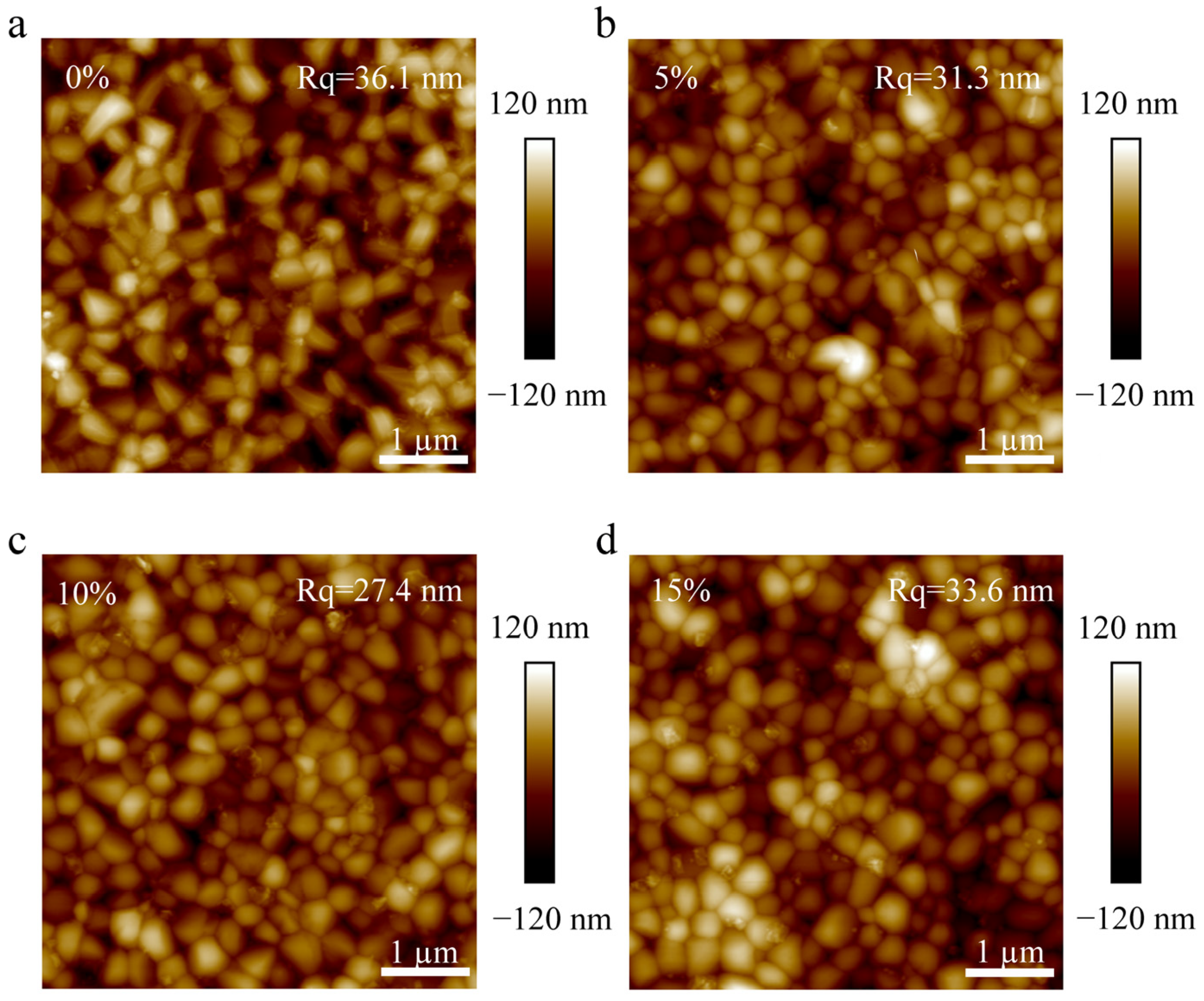
Atomic force microscopy (AFM) was carried out to study the effect of varying SnF2 additions on Sn–Pb perovskite films’ surface roughness. A lower root-mean-square roughness (Rq) is favorable for improving interfacial contact and suppressing interfacial recombination. As shown in Figure 2a, the control film without SnF2 exhibits a relatively rough surface with an Rq of 36.1 nm, indicating an inhomogeneous film surface. After introducing SnF2, the surface morphology of the Sn–Pb perovskite films is gradually improved. The Rq value decreases from 36.1 nm for the control film to 31.3 nm and 27.4 nm for the films with 5% and 10% SnF2, respectively. However, further increasing the SnF2 concentration to 15% leads to an increased Rq value of 33.6 nm. This result can be attributed to an appropriate amount of SnF2 suppressing Sn4+-induced defect formation, thereby improving the surface uniformity of Sn–Pb perovskite films, but excesses of 15% SnF2 cause the accumulation of residual SnF2 or F-rich species, resulting in the Rq value increasing [11]. Scanning electron microscopy (SEM) images further reveal that the incorporation of SnF2 addition slightly increases grain size and effectively suppresses defect formation, with less “white phase” formation associated with Sn2+ oxidation-induced [SnIx]2−x adduct formation (Figure S1, Supplementary Materials) [15,16]. In particular, the film with 10% SnF2 presented the most compact morphology and the lowest “white phase”, which is consistent with the AFM results. However, it seems that SnF2 unable to totally suppress Sn2+ oxidation indicating the limited antioxidant capability of a single SnF2 additive. To further quantify the Sn2+ oxidation degree, X-ray photoelectron spectroscopy (XPS) was performed. Evidence shows that SnF2 addition significantly suppresses Sn4+ formation, with a reduced peak area ratio of Sn4+/Sn2+ from 1.85 to 0.33 after SnF2 treatment.
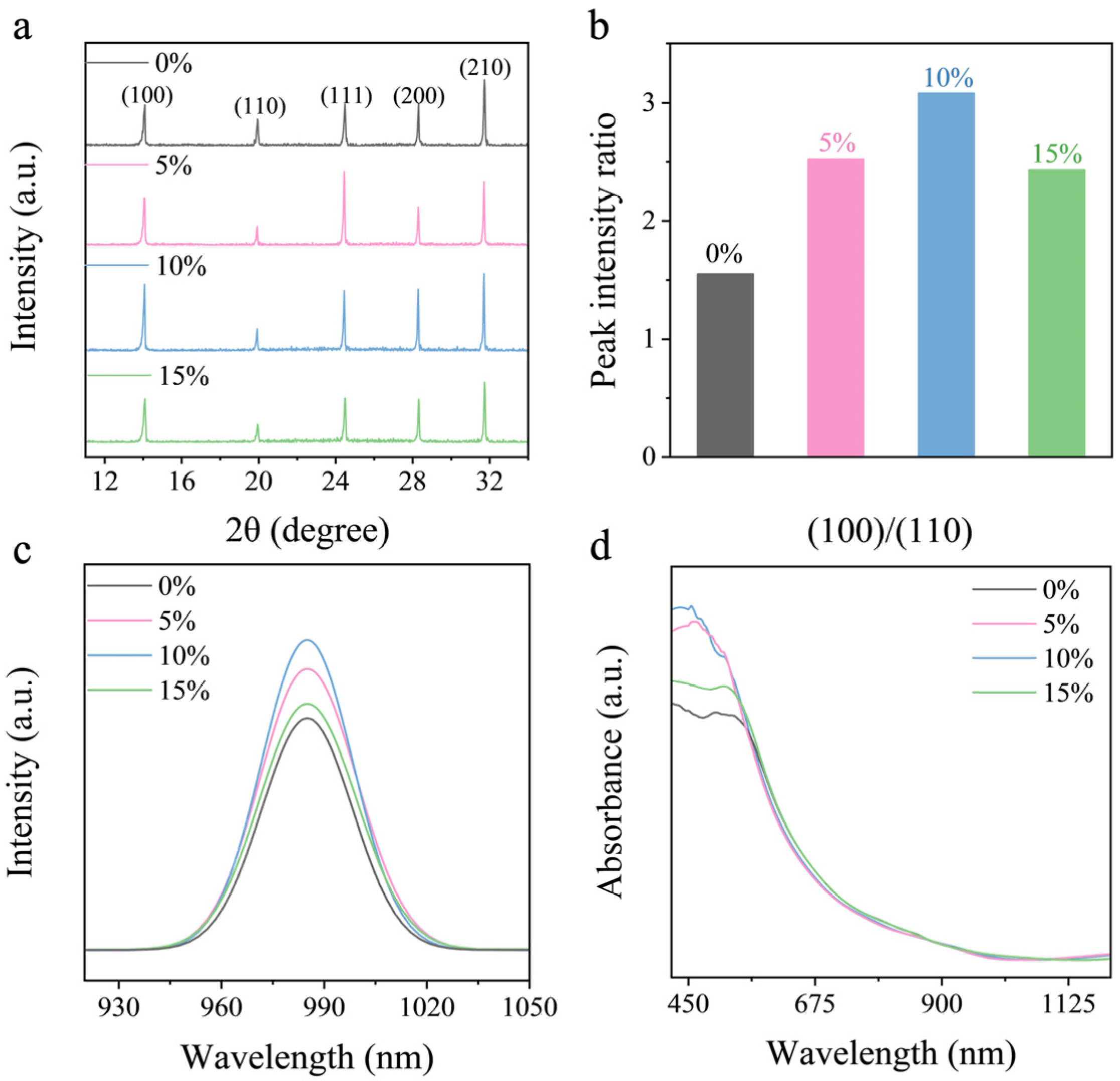
To investigate the influence of varying SnF2 amounts on the crystal structure and crystallinity of Sn–Pb perovskite films, X-ray diffraction (XRD) was carried out. As illustrated in Figure 3a, all films show identical diffraction peak positions, confirming that SnF2 does not significantly alter the main crystal structure. However, the diffraction intensities are visibly enhanced after the introduction of SnF2, indicating the improved crystallinity. Particularly, the film with 10% SnF2 showed the strongest diffraction peaks of (100) and (200), which is beneficial for carrier transfer and device efficiency according to previous reports [17,18,19]. This result is supported by the increased intensity ratio of the (100) diffraction peak for SnF2-treated films with respect to the control (I(100)_treated/I(100)_control), which exceeds 1 for all treated samples (Figure S2, Supplementary Materials). Moreover, the diffraction peak intensity ratio of (100)/(110) is further calculated, as shown in Figure 3b. The (100)/(110) ratios of all SnF2-treated films are higher than that of the control film, with the 10% SnF2 film showing the highest value. However, the highest relative intensities of (111)/(200) peaks are observed at 5% SnF2, suggesting different SnF2 concentrations preferentially promote different crystallographic orientations [20,21]. Therefore, these results indicate that an appropriate amount of SnF2 can optimize the crystallinity and orientation of Sn–Pb perovskite films, particularly at a concentration of 10%.
In Figure 3c, steady-state photoluminescence (PL) measurements were performed to evaluate the non-radiative recombination of Sn–Pb perovskite films. Sn–Pb perovskites with different SnF2 concentrations deposited on the glass substrate were excited from the film side using a 532 nm laser. As a result, all films treated with SnF2 exhibit enhanced PL intensities compared with the control film, suggesting suppressed defect-assisted non-radiative recombination after SnF2 is introduced. Furthermore, the UV–vis–NIR absorbance spectra show a similar trend after the introduction of SnF2, as shown in Figure 3d. The enhanced absorbance intensity of the SnF2-treated films indicates improved film quality, which can be attributed to optimized crystallization and more compact film morphology. It is worth mentioning that the corresponding Tauc plots show an optical bandgap of approximately 1.26 eV, which agrees well with the PL emission peak located at ~985 nm. This result further confirms that SnF2 incorporation does not change the bandgap and main crystal structure of Sn–Pb perovskite films (Figure S3, Supplementary Materials). The above results collectively confirm that the SnF2 additive, especially at 10% concentration, can effectively suppress Sn2+ oxidation induced defect formation, thereby optimizing the films’ morphology and crystallinity quality. Accordingly, the 10% SnF2-treated film is selected as the “Target” sample for subsequent device studies, while the pristine film without SnF2 is used as the “Control”.

3.2. Enhanced Device Performance

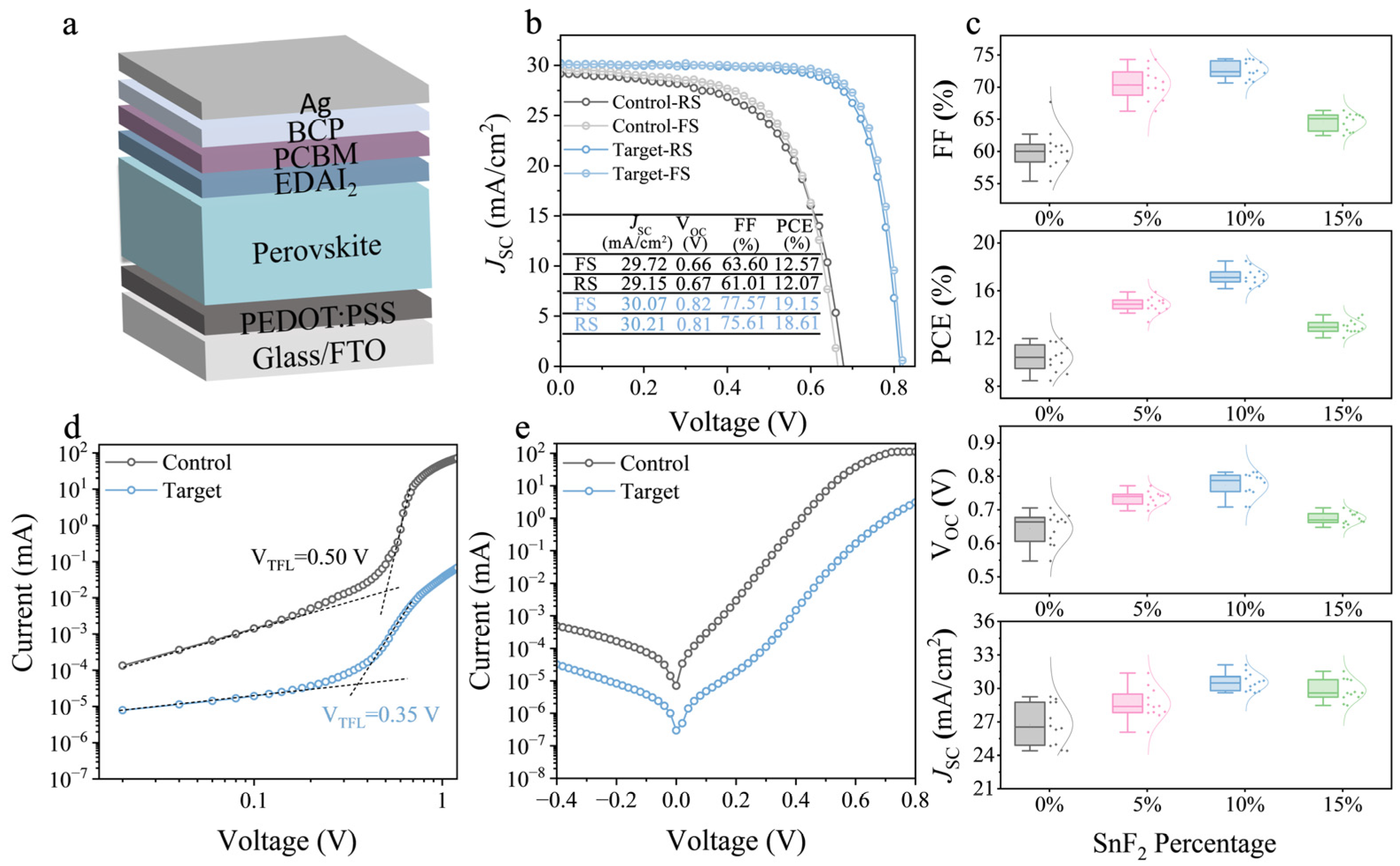
To further evaluate the effect of SnF2 additives on photovoltaic performance, as shown in Figure 4a, p-i-n Sn–Pb PSCs with a structure of FTO/PEDOT:PSS/FA0.85Cs0.15Pb0.5Sn0.5I3/EDAI2/PCBM/BCP/Ag were fabricated. As illustrated in Figure 4b, the control without SnF2 treatment presents a PCE of 12.57% under forward scan, with a short-circuit current density (JSC) of 29.72 mA/cm2, an open-circuit voltage (VOC) of 0.66 V and a fill factor (FF) of 63.60%. In contrast, the target device based on 10% SnF2 treatment presents a much higher PCE of 19.15% under forward scan, with a JSC of 30.07 mA/cm2, a VOC of 0.82 V and an FF of 77.57%. This performance is within the competitive values reported for Sn–Pb PSCs, and notably, it is achieved using SnF2 as the sole antioxidant additive (Table S2). The target device shows 52.34% enhancement in PCE compared with the control device, mainly owing to the significant improvement in VOC and FF. This improvement can be attributed to the optimized film’s quality, reduced defect density, and suppressed non-radiative recombination. Moreover, the SnF2-modified devices, particularly the target group, exhibit improved reproducibility, with a narrower and more concentrated statistical distribution of photovoltaic parameters compared with the control, which is consistent with the J–V results (Figure 4c and Table S1, Supplementary Materials).
To quantify the defect density in the Sn–Pb perovskite films, space-charge-limited current (SCLC) measurements were performed using the electron-only structure of FTO/SnO2/Sn–Pb perovskite/PCBM/Ag. As shown in Figure 4d, the trap-filled limit voltage (VTFL) decreases from 0.50 V for the control device to 0.35 V for the target device. The trap density (Ntrap) is calculated by the following equation:
N t r a p = 2 ε ε 0 V T F L e L 2
where ε, ε0, e, and L are the relative dielectric constant (~20), vacuum permittivity, elementary electric charge, and perovskite film thickness (~700 nm), respectively [22]. As a result, the target device exhibited a lower Ntrap, of 1.58 × 1015 cm−3, than the control (2.26 × 1015 cm−3) and other SnF2 concentrations, indicating reduced vacancies and defects of the Sn–Pb PSCs (Figure 4d and Figure S4, Supplementary Materials) [23]. Additionally, the target device exhibits nearly an order of magnitude lower reverse saturation current than the control, suggesting that the leakage current and non-radiative recombination are effectively suppressed by SnF2 modification, which is beneficial for improving the VOC of the target device (Figure 4e). A similar decrease in the reverse saturation current is also observed in other SnF2 concentrations (Figure S5, Supplementary Materials). Moreover, a smaller ideality factor is obtained after SnF2 treatment, confirming that most carriers are collected prior to recombination (Figure S6, Supplementary Materials).

4. Conclusions

In summary, we systematically investigated the effect of SnF2 concentrations on MA-free Sn–Pb perovskite films and the corresponding performance of devices. By meticulously studying the surface roughness, crystallization morphology, and optical properties of perovskite films, we found that the SnF2 additive significantly improved the films’ quality, with a smoother surface, improved crystallinity and fewer Sn2+ oxidation-related defects. Finally, the 10% SnF2 additive concentration is determined. Under the optimized parameters, the target device delivers a champion PCE of 19.15%, with a JSC of 30.07 mA/cm2, an FF of 77.57% and a VOC of 0.82 V, offering useful guidance for further improving the MA-free Sn-Pb PSCs’ performance.

Supplementary Materials

The following supporting information can be downloaded at: https://www.mdpi.com/article/10.3390/coatings16070805/s1, Figure S1: SEM images of Sn–Pb perovskite films with varying SnF2 concentration; Figure S2. XPS spectra of Sn 3d of Sn-Pb perovskite films with varying SnF2 treated; Figure S3: The intensity ratio of the (100) diffraction peak of the SnF2-treated perovskite films relative to that of the control film; Figure S4. Tauc plots of Sn–Pb perovskite films with varying SnF2 concentrations; Figure S5. SCLC curves of Sn–Pb PSCs containing 5% and 15% SnF2 additives; Figure S6. Dark J–V curves of Sn–Pb PSCs containing 5% and 15% SnF2 additives; Figure S7. Light-intensity-dependent VOC measurements of Sn–Pb perovskite solar cells with varying SnF2 treatment; Table S1: Comparison of photovoltaic parameters of MA-free Sn-Pb perovskite devices with representative reported works; Table S2. Statistical summary of photovoltaic parameters of 16 independent Sn–Pb PSCs with different SnF2 additive concentrations [21,24,25,26,27,28,29,30].

Author Contributions

Y.L.: Data Curation, Writing—Original Draft; J.H.: Conceptualization, Methodology; Q.C.: Investigation, Formal Analysis; F.X.: Validation, Writing—Reviewing and Editing; X.Z.: Supervision, Project Administration. All authors have read and agreed to the published version of the manuscript.

Funding

This research is supported by the National Natural Science Foundation of China (W2521086), Guangdong Basic and Applied Basic Research Foundation (2025A1515010515), Guangdong University of Technology SPOE Seed Foundation (SF2024111507) and 2025 Shanwei Talent Revitalization Plan for New Generation Electronic Information Industry (250421168940208). We would like to thank the Analysis and Test Center of Guangdong University of Technology for the surface analysis of our samples.

Data Availability Statement

Dataset available on request from the authors.

Conflicts of Interest

The authors declare no conflicts of interest.

References

  1. Guo, Y.; Yin, M.; Gao, H.; Ou, W.; Wu, P.; Liu, C.; Xia, S.; Zheng, X.; Luo, H.; Hong, J.; et al. Homogeneous Crystallization via Sustained Solvent-Extraction Channels for Methylammonium-Free All-Perovskite Tandem Solar Cells. Nat. Commun. 2026, 17, 1470. [Google Scholar] [CrossRef]
  2. Ma, T.; Zhao, X.; Yang, X.; Yan, J.; Luo, D.; Li, M.; Li, X.; Chen, C.; Song, H.; Tang, J. Inhibiting Ion Migration and Oxidation in Sn–Pb Perovskite by Multidentate Chelating Additive Strategy. Adv. Funct. Mater. 2025, 35, 2412216. [Google Scholar] [CrossRef]
  3. Ge, C.; Jiang, B.; Zhu, J.; Zhang, P.; Ma, R.; Yan, S.; Liu, Z.; Shaker, A.; Salem, M.S.; Luo, J.; et al. Efficient Sn–Pb Mixed Perovskite Solar Cells Via Minimizing Solvent Oxidation. Adv. Funct. Mater. 2024, 34, 2400075. [Google Scholar] [CrossRef]
  4. Chang, X.; Yang, G.; Chen, H.; Cao, J.; Zhong, J.; Tan, Y.; Yang, M.; Jin, B.; Wu, C.; Li, S.; et al. Cyclically Dynamic Defect Management Enables High-efficiency Sn–Pb Perovskite Photovoltaics with Enhanced Photostability and Fatigue Resistance. Angew. Chem. 2025, 65, e14563. [Google Scholar] [CrossRef]
  5. Bati, A.S.R.; Liu, C.; Gilley, I.W.; Musgrave, C.B.; Maxwell, A.; Steele, J.A.; Yang, Y.; Chen, H.; Wan, H.; Xu, J.; et al. A Chemically Bonded Monolayer Interface Enables Enhanced Thermal Stability and Efficiency in Pb-Sn Perovskite Solar Cells. Joule 2025, 9, 102047. [Google Scholar] [CrossRef]
  6. Kumar, M.H.; Dharani, S.; Leong, W.L.; Boix, P.P.; Prabhakar, R.R.; Baikie, T.; Shi, C.; Ding, H.; Ramesh, R.; Asta, M.; et al. Lead-Free Halide Perovskite Solar Cells with High Photocurrents Realized Through Vacancy Modulation. Adv. Mater. 2014, 26, 7122–7127. [Google Scholar] [CrossRef] [PubMed]
  7. Li, T.; Luo, X.; Wang, P.; Li, Z.; Li, Y.; Huang, J.; Jin, Z.; Yang, Y.; Li, B.; Zhang, W.; et al. Tin-Based Perovskite Solar Cells with a Homogeneous Buried Interface. Nature 2025, 648, 84–90. [Google Scholar] [CrossRef] [PubMed]
  8. Lin, R.; Gao, H.; Lou, J.; Xu, J.; Yin, M.; Wu, P.; Liu, C.; Guo, Y.; Wang, E.; Yang, S.; et al. All-Perovskite Tandem Solar Cells with Dipolar Passivation. Nature 2025, 648, 600–606. [Google Scholar] [CrossRef] [PubMed]
  9. Chen, Q.; Luo, J.; He, R.; Lai, H.; Ren, S.; Jiang, Y.; Wan, Z.; Wang, W.; Hao, X.; Wang, Y.; et al. Unveiling Roles of Tin Fluoride Additives in High-Efficiency Low-Bandgap Mixed Tin-Lead Perovskite Solar Cells. Adv. Energy Mater. 2021, 11, 2101045. [Google Scholar] [CrossRef]
  10. Zillner, J.; Boyen, H.; Schulz, P.; Hanisch, J.; Gauquelin, N.; Verbeeck, J.; Küffner, J.; Desta, D.; Eisele, L.; Ahlswede, E.; et al. The Role of SnF2 Additive on Interface Formation in All Lead-Free FASnI3 Perovskite Solar Cells. Adv. Funct. Mater. 2022, 32, 2109649. [Google Scholar] [CrossRef]
  11. Kurisinkal Pious, J.; Zwirner, Y.; Lai, H.; Olthof, S.; Jeangros, Q.; Gilshtein, E.; Kothandaraman, R.K.; Artuk, K.; Wechsler, P.; Chen, C.; et al. Revealing the Role of Tin Fluoride Additive in Narrow Bandgap Pb-Sn Perovskites for Highly Efficient Flexible All-Perovskite Tandem Cells. ACS Appl. Mater. Interfaces 2023, 15, 10150–10157. [Google Scholar] [CrossRef] [PubMed]
  12. Wang, J.; Dang, W.; Zhang, Y.; Zhang, C.; Hu, Z.; Zhang, X.; Tian, Y.; Xu, K.; Guo, Q.; Chao, L.; et al. Homogeneous SnF2-Induced Strain Modulation in Sn–Pb Perovskites for High-Performance Monolithic All-Perovskite Tandem Solar Cells. Angew. Chem. Int. Ed. 2026, 65, e15733. [Google Scholar] [CrossRef] [PubMed]
  13. Gao, H.; Wen, J.; Zhao, S.; Li, M.; Yang, S.; Sun, H.; Liu, C.; Xia, S.; Nguyen, K.; Wu, P.; et al. Crystallization Modulation of Methylammonium-Free Narrow-Bandgap Perovskite for Thermal-Stable All-Perovskite Tandem Solar Modules. Sci. Adv. 2026, 12, eadz9089. [Google Scholar] [CrossRef] [PubMed]
  14. Huang, B.; Zheng, L.; Hu, R.; Xuan, Y. Suppressing Sn-Rich Phase Precipitation Enables Controlled Crystallization in MA-Free Sn–Pb Perovskite Solar Cells. ACS Energy Lett. 2026, 11, 4055–4066. [Google Scholar] [CrossRef]
  15. Zhou, Y.; Huang, X.; Zhang, J.; Zhang, L.; Wu, H.; Zhou, Y.; Wang, Y.; Wang, Y.; Fu, W.; Chen, H. Interfacial Modification of NiOx for Highly Efficient and Stable Inverted Perovskite Solar Cells. Adv. Energy Mater. 2024, 14, 2400616. [Google Scholar] [CrossRef]
  16. Pascual, J.; Flatken, M.; Félix, R.; Li, G.; Turren-Cruz, S.; Aldamasy, M.H.; Hartmann, C.; Li, M.; Di Girolamo, D.; Nasti, G.; et al. Fluoride Chemistry in Tin Halide Perovskites. Angew. Chem. Int. Ed. 2021, 60, 21583–21591. [Google Scholar] [CrossRef] [PubMed]
  17. Li, J.; Duan, J.; Zhang, C.; Qi, Z.; Liu, Y.; Duan, X.; Liu, Y.; Dou, J.; Guo, Q.; He, B.; et al. Facet-Orientation-Enhanced Thermal Transfer for Temperature-Insensitive and Stable p-i-n Perovskite Solar Cells. eScience 2025, 5, 100372. [Google Scholar] [CrossRef]
  18. Liu, Z.; Lin, R.; Wei, M.; Yin, M.; Wu, P.; Li, M.; Li, L.; Wang, Y.; Chen, G.; Carnevali, V.; et al. All-Perovskite Tandem Solar Cells Achieving >29% Efficiency with Improved (100) Orientation in Wide-Bandgap Perovskites. Nat. Mater. 2025, 24, 252–259. [Google Scholar] [CrossRef] [PubMed]
  19. Karim, M.A.; Ahmmed, S.; Cao, S.; Kayesh, M.E.; He, Y.; Rahman, M.A.; Chowdhury, W.I.; Yanagida, M.; Shirai, Y.; Islam, A. Chelating Coordination Regulates Perovskite Crystallization and Defect Passivation in Sn–Pb Perovskite Solar Cells. Small 2026, 20, e00050. [Google Scholar] [CrossRef] [PubMed]
  20. Shen, X.; Gallant, B.M.; Holzhey, P.; Smith, J.A.; Elmestekawy, K.A.; Yuan, Z.; Rathnayake, P.V.G.M.; Bernardi, S.; Dasgupta, A.; Kasparavicius, E.; et al. Chloride-Based Additive Engineering for Efficient and Stable Wide-Bandgap Perovskite Solar Cells. Adv. Mater. 2023, 35, 2211742. [Google Scholar] [CrossRef] [PubMed]
  21. Chen, B.; Yu, Z.; Onno, A.; Yu, Z.; Chen, S.; Wang, J.; Holman, Z.C.; Huang, J. Bifacial All-Perovskite Tandem Solar Cells. Sci. Adv. 2022, 8, eadd0377. [Google Scholar] [CrossRef] [PubMed]
  22. Lai, Y.; Xu, X.; Tang, X.; Li, P.; Chen, H.; Zhu, H.; Peng, R.; Yang, L.; Jia, Z.; Hui, J.; et al. Multifunctional Passivator Enables High-Efficient Gas-Quenching Sn–Pb Perovskite Solar Cells. ACS Energy Lett. 2025, 10, 4131–4139. [Google Scholar] [CrossRef]
  23. Zheng, B.; Liu, H.; Cao, Q.; Liu, C.; Xing, J.; Ma, L.; Zhang, X. Co-Adsorption Strategies on NiO/Perovskite Buried Interface for Efficient Perovskite Solar Cells. Surf. Interfaces 2025, 72, 107246. [Google Scholar] [CrossRef]
  24. Klug, M.T.; Milot, R.L.; Patel, J.B.; Green, T.; Sansom, H.C.; Farrar, M.D.; Ramadan, A.J.; Martani, S.; Wang, Z.; Wenger, B.; et al. Metal Composition Influences Optoelectronic Quality in Mixed-Metal Lead–Tin Triiodide Perovskite Solar Absorbers. Energy Environ. Sci. 2020, 13, 1776–1787. [Google Scholar] [CrossRef]
  25. Liu, H.; Sun, J.; Hu, H.; Li, Y.; Hu, B.; Xu, B.; Choy, W.C.H. Antioxidation and Energy-Level Alignment for Improving Efficiency and Stability of Hole Transport Layer-Free and Methylammonium-Free Tin–Lead Perovskite Solar Cells. ACS Appl. Mater. Interfaces 2021, 13, 45059–45067. [Google Scholar] [CrossRef] [PubMed]
  26. Tong, J.; Gong, J.; Hu, M.; Yadavalli, S.K.; Dai, Z.; Zhang, F.; Xiao, C.; Hao, J.; Yang, M.; Anderson, M.A.; et al. High-performance methylammonium-free ideal-band-gap perovskite solar cells. Matter 2021, 4, 1365–1376. [Google Scholar] [CrossRef]
  27. Jiang, T.; Xu, X.; Lan, Z.; Chen, Z.; Chen, X.; Liu, T.; Huang, S.; Yang, Y. Efficient MA-free Pb-Sn Alloyed Low-Bandgap Perovskite Solar Cells via Surface Passivation. Nano Energy 2022, 101, 107596. [Google Scholar] [CrossRef]
  28. Pitaro, M.; Alonso, J.S.; Di Mario, L.; Romero, D.G.; Tran, K.; Zaharia, T.; Johansson, M.B.; Johansson, E.M.J.; Loi, M.A. A Carbazole-Based Self-Assembled Monolayer as the Hole Transport Layer for Efficient and Stable Cs0.25FA0.75Sn0.5Pb0.5I3solar cells. J. Mater. Chem. A 2023, 11, 11755–11766. [Google Scholar] [CrossRef]
  29. Pitaro, M.; Alonso, J.E.S.; Di Mario, L.; Romero, D.G.; Tran, K.; Kardula, J.; Zaharia, T.; Johansson, M.B.; Johansson, E.M.J.; Chiechi, R.C.; et al. Tuning the Surface Energy of Hole Transport Layers Based on Carbazole Self-Assembled Monolayers for Highly Efficient Sn/Pb Perovskite Solar Cells. Adv. Funct. Mater. 2023, 34, 2306571. [Google Scholar] [CrossRef]
  30. Ma, Y.; Zheng, F.; Li, S.; Liu, Y.; Ren, J.; Wu, Y.; Sun, Q.; Hao, Y. Regulating the Crystallization Growth of Sn–Pb Mixed Perovskites Using the 2D Perovskite (4-AMP)PbI4 Substrate for High-Efficiency and Stable Solar Cells. ACS Appl. Mater. Interfaces 2023, 15, 34862–34873. [Google Scholar] [CrossRef] [PubMed]
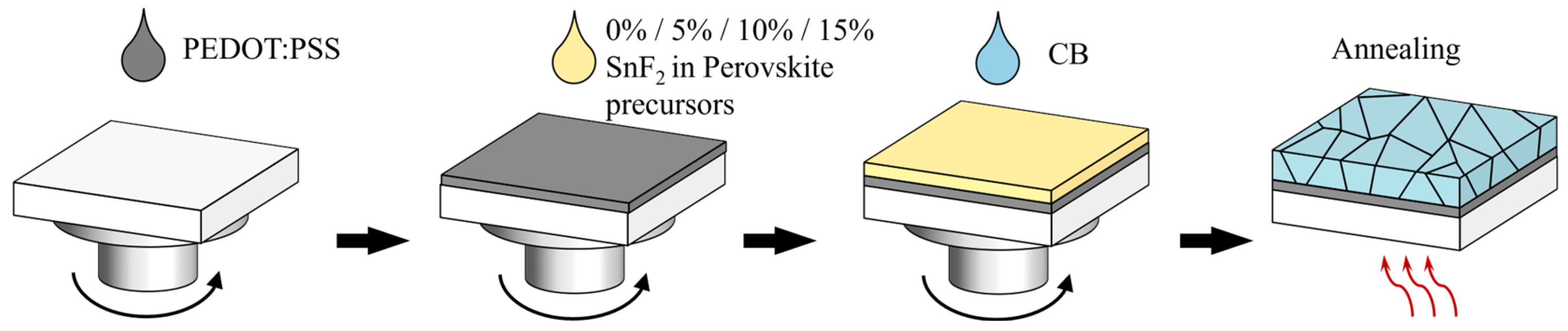
Figure 1. Schematic illustration of the fabrication process of Sn–Pb perovskite films.
Coatings 16 00805 g001
Figure 2. AFM images of Sn–Pb perovskite films with different SnF2 concentrations: (a) 0%, (b) 5%, (c) 10%, and (d) 15% relative to SnI2.
Coatings 16 00805 g002
Figure 3. (a) XRD patterns, (b) corresponding peak intensity ratios of (100)/(110), (c) steady-state PL patterns, and (d) UV–vis–NIR absorbance spectra of Sn–Pb perovskite films with varying SnF2 concentrations.
Coatings 16 00805 g003
Figure 4. (a) Schematic illustration of the inverted Sn–Pb PSC architecture. (b) Champion J–V curves of the control and target devices. (c) Statistical distribution of the photovoltaic parameters of Sn–Pb PSCs with varying SnF2 concentrations. (d) SCLC and (e) dark J–V measurements for the control and target devices.
Coatings 16 00805 g004
Disclaimer/Publisher’s Note: The statements, opinions and data contained in all publications are solely those of the individual author(s) and contributor(s) and not of MDPI and/or the editor(s). MDPI and/or the editor(s) disclaim responsibility for any injury to people or property resulting from any ideas, methods, instructions or products referred to in the content.