Article

Design Method for Stress Reduction of Multilayer Thin Films

Xi’an Institute of Applied Optics, Xi’an 710065, China
*
Author to whom correspondence should be addressed.
Coatings 2025, 15(9), 980; https://doi.org/10.3390/coatings15090980
Submission received: 29 July 2025 / Revised: 16 August 2025 / Accepted: 19 August 2025 / Published: 22 August 2025
(This article belongs to the Section Thin Films)

Abstract

Residual stress in optical thin films severely degrades optoelectronic device performance. Traditional designs, relying on extensive experiments, limit precise stress regulation. This study proposes a Stoney’s formula-based stress design method for multilayer thin films, constructing a mathematical model to characterize their total stress. Innovatively, it integrates single-layer stress and spectral performance for dual-objective optimization (stress elimination and spectral indicators), significantly reducing deposition workload. Experiments show small stress-prediction deviations in the 1.064 μm laser and 3.7–4.8 μm mid-infrared bands. A 16-layer broadband antireflection film (400–900 nm) with Ti2O3, HfO2, and SiO2 also shows effectively reduced stress. This model offers a novel, reliable scheme for precise residual stress regulation in multilayer thin films.

1. Introduction

Stress in optical thin films significantly impacts the performance of thin-film devices and the reliability of film layers, potentially causing issues such as surface deformation, film cracking, and delamination [1,2,3]. In engineering applications, measures to minimize stress typically include optimizing film preparation parameters through numerous deposition experiments, using bonding layers or transition layers to match stress during multilayer deposition, and superimposing films with different stress types (tensile or compressive) to offset stress [4,5,6]. However, these traditional methods rely heavily on extensive deposition trials and fail to precisely predict the stress states of the entire film system, limiting their efficiency in practical applications.
This study differs from and advances existing research by shifting the focus from an experimental trial-and-error approach to model-based prediction and optimization. While previous works have explored stress reduction through process optimization (e.g., adjusting substrate temperature, deposition rate, or background vacuum [7,8,9,10,11]), they lack a systematic framework to integrate stress characteristics with spectral performance. In contrast, our approach establishes a mathematical model for multilayer thin-film stress based on Hoffman’s grain boundary model [12], which describes stress generation from intergranular interactions, and Stoney’s formula [13,14,15], which enables stress calculation by relating substrate curvature changes to film stress. By integrating single-layer film stress and spectral performance into a dual-objective optimization (stress elimination and spectral indicators) for film-system structure, this method achieves precise stress prediction and reduces the need for excessive deposition experiments [12,13,14,15].
This approach not only improves the success rate of thin-film research but also offers new insights for optical thin-film design, device development, film preparation, and engineering manufacturing, addressing the limitations of traditional methods that lack quantitative integration of stress and spectral performance [4,5,6].

2. Methods

A multilayer film system typically consists of at least two different materials, where the stress of each layer affects the final stress state of the entire system. Factors influencing layer stress are complex, including deposition methods, material properties, deposition process parameters, and post-treatment. To minimize stress after deposition, extensive efforts are usually made to optimize processes (e.g., substrate temperature, deposition rate, background vacuum, process gas flow, and auxiliary ion sources) under appropriate deposition methods [7,8,9,10,11]. While effective, this approach is cumbersome due to the need for numerous experiments. To simplify preparation, stress elimination in the entire multilayer system can be achieved by optimizing the film structure during design.
For a multilayer system composed of different materials, assume that the stress per unit thickness of each layer is σ1/h1, σ2/h2, σ3/h3, …, and their corresponding thicknesses are h1, h2, h3, …. The substrate deforms under the total stress of the entire film system, and the total stress generated by the films is as follows:
σ = i = 1   σ i = i = 1   q i h i
where σ i , h i , and q i represent the stress magnitude of the ith layer membrane, the thickness of the membrane layer, and the stress magnitude of membrane layer per unit thickness, respectively.
According to Hoffman’s grain boundary model, internal film stress arises from intergranular interactions. During film growth, atoms stack, and the distance between grains reduces to the lattice constant. Attraction between surface atoms of adjacent grains causes strain at grain contacts, forming grain boundaries. The grain boundary potential energy can be equivalent to strain energy, defined as the difference between the surface free energy of two grains and the net grain boundary potential energy. When grains bond, surface energy relaxation compresses grain surfaces, leading to grain stretching. The grain boundary deformation is Δ, and the stress generated in grains [12] is as follows:
σ = E ( 1 ν ) Δ d
where d is the grain size, E is the Young’s modulus of the substrate, and ν is the Poisson’s ratio of the substrate. For a single-layer film on a homogeneous substrate, the stress in the single-layer film is calculated based on Stoney formula, σ f [13,14,15]:
σ f = 1 6 E s ( 1 ν s ) h s 2 h f 1 R
where h s is the thickness of the substrate; h f is the thickness of the film; E s is the modulus of the style of the substrate; ν s is the Poisson’s ratio of the substrate; 1 R = 1 R f 1 R s is the variable of the radius of curvature (As shown in Figure 1); R s and R f are the radius f curvature before and after coating, respectively; and all of them are measurable quantities.
For a multilayer film system with a membrane structure of S u b / a 1 A / b 1 B / a 2 A / c 1 C / a 3 A / b 2 B / A i r , where S u b denotes the substrate; A , B , C represent the thin-film materials; a i , b i , c i denote the thicknesses of the film layers, respectively; i = 1 , 2 , 3 m ; and A i r indicates the surrounding medium (air). In the actual preparation of thin films, except for the film that is deposited on the substrate, each subsequent layer of film is deposited on top of the previous layer. Therefore, the stress condition of each layer of film in a multilayer system is influenced by the previous layer of film. Let σ 0 , 1 , σ 1 , 2 , σ 2 , 3 ⋯⋯ σ m 1 , m denote the stress magnitude of the first, second, third… mth layer of film, and q 0 , 1 , q 1 , 2 , q 2 , 3 ⋯⋯ q m 1 , m denote the stress magnitude per unit thickness of the film layer from the first, second, third… mth layer of film, and the total stress that the substrate receives from the film layer is as follows:
σ = i = 1 m σ i 1 , i = i = 1 m q i 1 , i h i
If the multilayer film is equivalent to a composite film, the stress magnitude ( σ ) of the equivalent composite film, the average stress ( q ) of the unit thickness of the equivalent film, the total thickness of the film layer, and the deformation of the curvature radius of the final part ( R Δ ) can be expressed as follows:
σ = 1 6 E s ( 1 ν s ) h s 2 h 1 R Δ
where 1 R Δ = 1 R fm 1 R s , according to (4) and (5):
σ = i = 1 m σ i 1 , i h i = q h
1 R Δ = i = 1 m 1 R i   = i = 1 m 1 R i 1 R i 1   = 1 R m 1 R 0
R i represents the amount of change in the radius of curvature of the substrate caused by the i th layer film, as shown in the Figure 2.
In theory, under the condition of a stable film deposition process, the stress after each film deposition can be considered a definite value. Therefore, in actual engineering, it is only necessary to measure A ,   B ,   C , the stress of various films deposited on different substrates; establish a stress database, σ i , j , for single-layer films; and then the stress of the film can function as one of the targets for the structural optimization of the film system when designing the film system, so as to achieve the purpose of stress-free design of multilayer films.
σ i , j = σ 0 , a ,   σ 0 , b ,   σ 0 , c σ a , b ,   σ a , c ,   σ a , d σ b , a ,   σ b , c ,   σ b , d σ c , a ,   σ c , b ,   σ c , d
The objective function for the stress in the design of multilayer films is therefore as follows:
F σ = min i = 1 n σ i 1 , i h i
Considering the spectral index requirements for film design, assuming that C ( λ ) is the calculated value of the transmittance at the target wavelength, T ( λ ) is the target value for transmittance design, N ( λ ) is the normalization factor, m is the target number, and n is the number of film layers, we denote that C ( λ ) T ( λ ) indicates the magnitude of the deviation from the target value of the transmittance at the wavelength. The sum of the target deviations for the spectral transmittance at all wavelengths within the designed working wavelength band is integrated, and the normalized mean value is 1 m λ = 1 m C ( λ ) T ( λ ) N ( λ ) . In practice, the range of the designed wavelength band is usually a continuous wavelength, and the deviation value function of the spectral transmittance is obtained by summation and integration:
F λ = 1 m λ = 1 m C ( λ ) T ( λ ) N ( λ ) d λ
When designing multilayer systems, it is necessary to optimize the structure of the multilayer system to meet the spectral performance index and the requirement of stress-free film layer under the condition of considering the realizability of the film layer preparation process:
F ( T , h , σ ) = min 1 m λ = 1 m C ( λ ) T ( λ ) N ( λ ) d λ , min i = 1 n σ i 1 , i h i
In practical engineering applications, the optimization of the membrane structure is achieved when the deviation values of the membrane stress and spectral transmittance in the above objective function reach a certain range.

3. Numerical Calculation and Experimental Test

3.1. Stress–Thickness Relationship Verification of Single-Layer Film

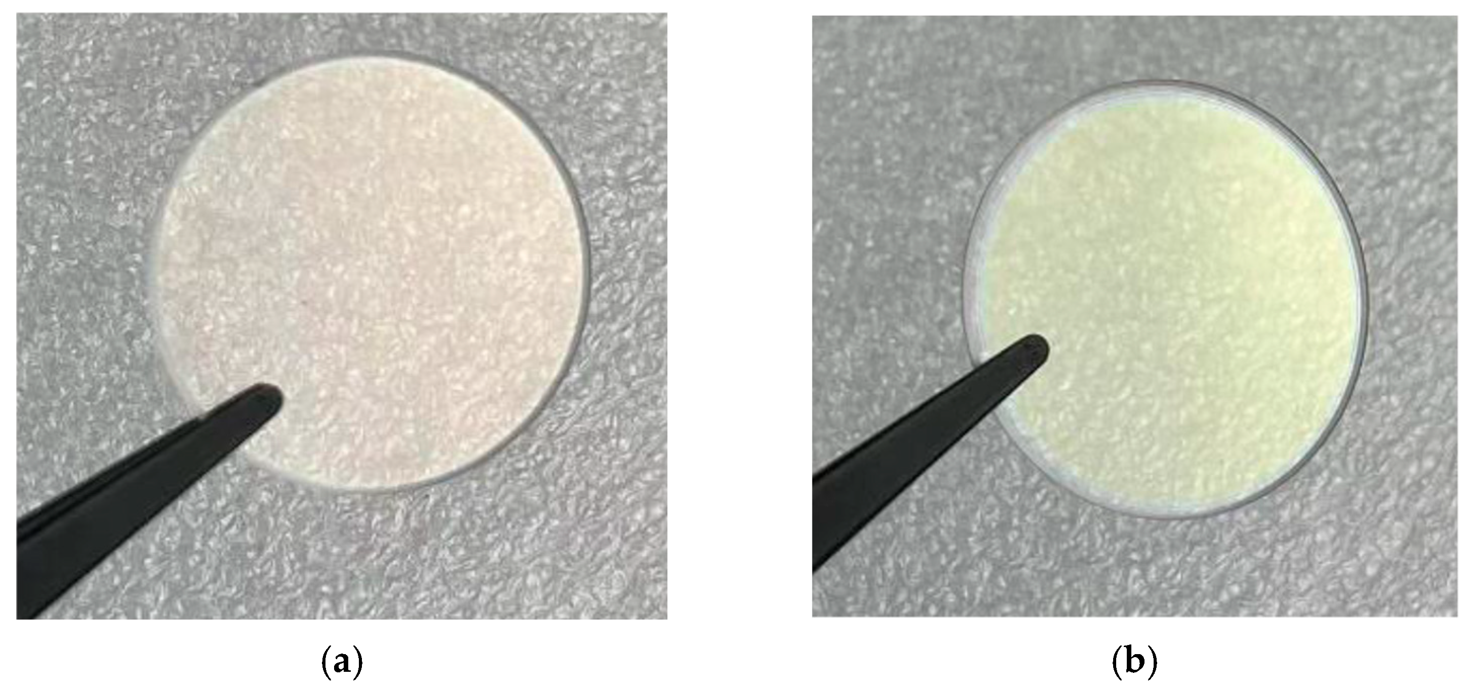
In order to verify the theoretical model of stress multilayer films described above, the linear relationship between the stress in the film and the thickness is first verified. ITO films with thicknesses of 120 nm and 250 nm were deposited on quartz substrates using the same process parameters, and the specific parameters are as shown in Table 1.
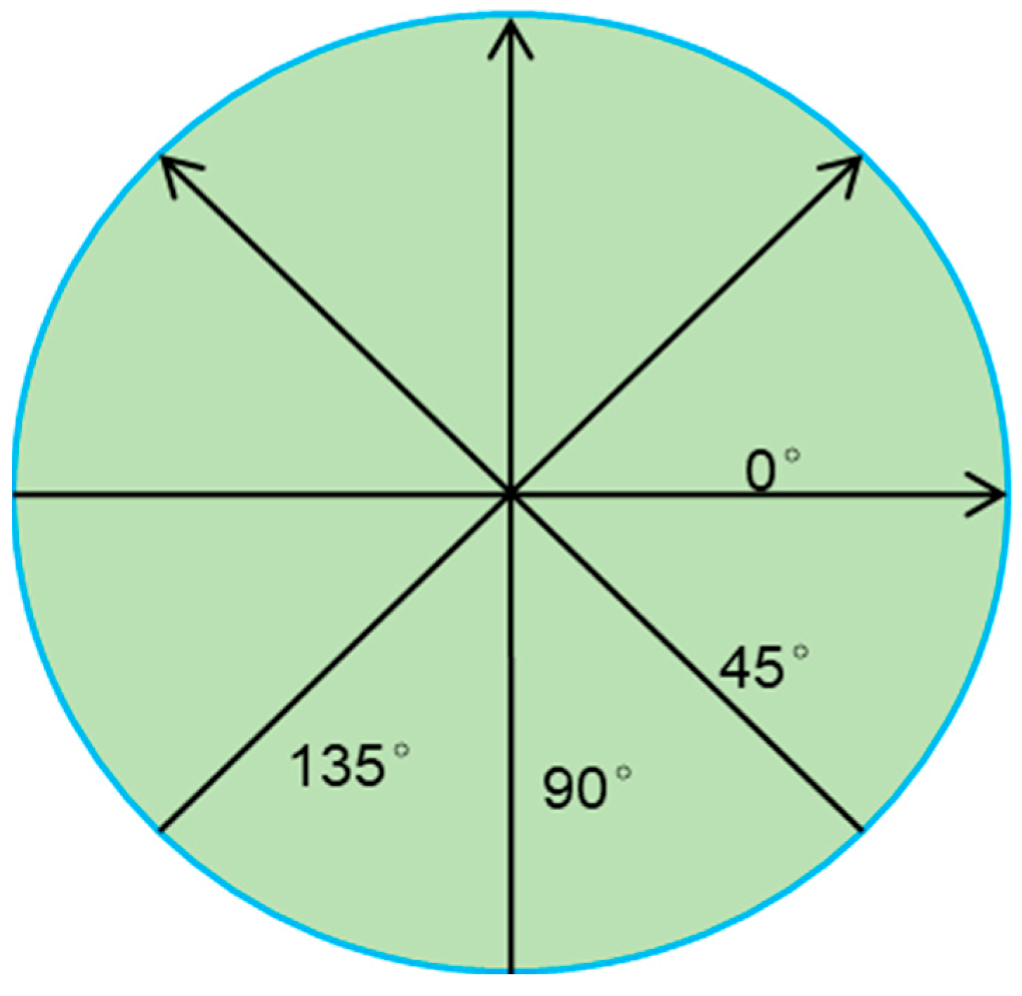
The film stress is tested by the FST5000 film stress meter, with a laser wavelength of 635 nm, scanning at 45° intervals, and with a scanning step of 2 mm. The test process is carried out in a clean room, the test environment temperature is controlled at (22 ± 1) °C, the relative humidity is 45%–65%, and there is no obvious vibration source near the test area. The test scheme is shown in the Figure 3.
During the experiment, the substrate without coating is scanned and tested first to obtain the bow height and curvature of the substrate pre-coating surface, and then the coating is deposited on the substrate (As shown in Figure 4); the bow height and curvature of the surface after coating are scanned and tested; and, finally, the test values after and before coating are subtracted, and the of the coating is calculated according to the subtraction results of the curvature and the thickness of the coating.
From the stress tests of the two ITO film samples with different thicknesses, we determined that the thickness ratio is 250:120 = 2.08, and the ratio of the measured stress values of the film layers is 1171.38:527.01 = 2.22. The deviation of the two is about 6.6%, and it can be considered that the consistency of the film layer’s stress and thickness relationship is good.

3.2. Multilayer Film Design and Verification

To verify that the stress of multilayer films composed of different materials conforms to the theoretical model, a multilayer film is deposited on a sapphire substrate via plasma-assisted electron beam evaporation. The final stress of the multilayer film is tested by comparing it with the calculated value of the theoretical model. A multilayer film composed of Ti2O3 and SiO2 is deposited on a sapphire substrate with a thickness of 0.5, a diameter of 71 mm, and double-sided polishing via plasma-assisted electron beam evaporation. The spectral requirement is ρ ¯ 2 % for the residual reflectance of a 1064 um laser and a mid-infrared dual band of 3.7 μm–4.8 μm, with a wide angle of incidence of 0–55, and the film stress is less than σ 80   MPa . Sapphire’s Young’s modulus is about 380 GPa, and its Poisson’s ratio is about 0.28. The specific parameters are as Table 2.
The stress of the single-layer TiO3 and single-layer SiO2 films deposited on sapphire substrate is as shown in Figure 5 and Table 3.
When designing the film system’s structure, an initial six-layer configuration (denoted as Sub/Ti2O3/SiO2/Ti2O3/SiO2/Ti2O3/SiO2/Air) was first proposed, where each layer alternates between Ti2O3 and SiO2 films with optical thicknesses of λ0/4 (quarter-wave optical thickness) for the respective materials, and λ0 is the reference wavelength. To optimize the film structure according to spectral requirements, the transmittance T(λ) is replaced with reflectance ρ(λ). By incorporating the angle of incidence, θ, the objective function for film-system optimization is formulated as follows:
F ( θ , λ , h , σ ) = θ = 0 55 C ( 1.064   um , θ ) 2 % N ( 1.064   um , θ ) + 1 1.1   um λ = 3.7   um 4.8   um C ( λ , θ ) 2 % N ( λ , θ ) d λ d θ 0 i = 1 n σ i 1 , i h i 80   MPa
The calculated value, C ( λ , θ ) , of the reflectivity can be calculated from the characteristic matrix of the multilayer film, and the equivalent admittance of the film system is
Y ( λ , θ ) = A ( λ , θ ) B ( λ , θ )
B ( λ , θ ) A ( λ , θ ) = j = 1 m cos δ j i η j sin δ j i η j sin δ j cos δ j 1 η G
The reflectivity at an angle a of incidence is calculated at θ wavelength λ to be as follows:
C ( λ , θ ) = 1 A ( λ , θ ) B ( λ , θ ) 1 + A ( λ , θ ) B ( λ , θ ) × 1 A ( λ , θ ) B ( λ , θ ) 1 + A ( λ , θ ) B ( λ , θ )
In the above equation: δ j = 2 π λ n j d j cos θ j is the phase thickness of the jth layer film; η G = 4.1 is the admittance of the substrate; λ is the wavelength; n j d j is the optical thickness of the jth layer film; n j is the refractive index of the jth layer film; and θ j is angle of incidence.
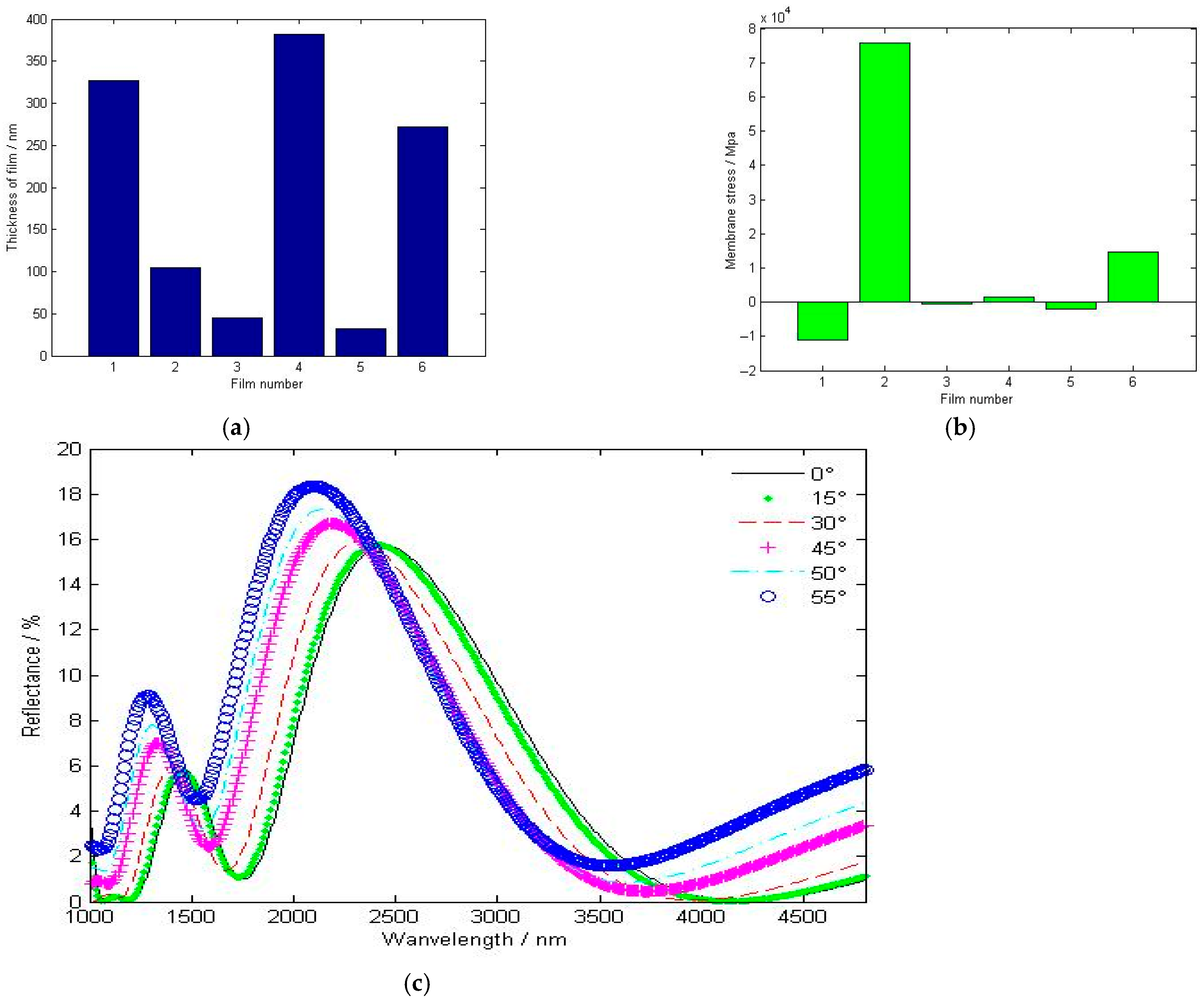
The multilayer structure is optimized by the above method, and the thickness distribution of the optimized multilayer structure becomes S u b / 327.1 T i 2 O 3 / 104.9 S i O 2 / 44.5 T i 2 O 3 / 382.3 S i O 2 / 32.3 T i 2 O 3 / 271.9 S i O 2 / A i r . The total thickness of the film layer is h f = 1163   nm . Where the number in front of Ti2O3 and SiO2 film represents the thickness of the film layer, the unit is nm; Air represents the medium around the incident surface, and Sub represents the substrate (sapphire). The thickness distribution and the remaining reflectivity curve of the multilayer structure are shown in Figure 6.
The membrane system stress value is calculated to be 70.424 Mpa according to Formula (6), which is a tensile (positive stress). The deposition process of the membrane layer is carried out by using a Beijing Buehler Leybold(Beijing, China) ARES-1550 type electronic beam evaporation coating machine, and the workpiece frame is a four-piece planetary disk. There are uniformity correction baffles for the thickness of the membrane layer on both evaporation sources at Φ500 mm, and the non-uniformity of the thickness of the membrane layer is less than 0.5%. The vacuum system uses a Lebold vacuum mechanical pump, roots pump, double diffusion pump, and cryogenic trap. The cryogenic trap maintains a temperature of about −120 °C when it works, the background vacuum degree during the coating process is about 2.0 × 10⁻⁶ mbar. During the experiment, for the same kind of thin-film material, the deposition process conditions (such as background vacuum degree, baking temperature, deposition rate, auxiliary ion parameters, uniformity modification screen, etc.) were maintained the same in all film structures to ensure that the effectiveness of the stress of each layer of film was maintained. The specific deposition processes are shown in Table 4.
The testing process was carried out in a clean laboratory, the ambient temperature was controlled within the range of (22 ± 1) °C, the relative humidity was 45%–65%, and there was no vibration source near the testing area. The results of the test are shown in Figure 7, Figure 8 and Figure 9, including the actually measured average stress value tensile stress (i.e., positive stress), and the magnitude is 74.61 MPa.
Figure 7 shows the arching height at different locations on the surface of the tested parts, where four different locations are selected for scanning test at equal angular intervals the test. Figure 7a,b show the arching height curves and 3D morphology of the substrate surface shape before coating, Figure 7c,d show the arching height curves and 3D morphology after coating, and Figure 7e,f show the data of the difference between the arching heights before after coating.
Figure 8 shows the curvature of the test parts at different locations on the surface. Figure 8a depicts the curvature of the substrate before coating, Figure 8b depicts the curvature after coating, and Figure 8c shows the data obtained by subtracting the curvature before and after coating.
To further verify the design effect of more layers of film, the 400 nm–900 nm broadband antireflection film on the K substrate is designed as an example. The antireflection film of 400 nm–900 nm is designed on the optical window, with an average remaining reflect of less than 0.5%. In order to ensure the good durability of the film layer on the optical window, the stress of the film layer is required to be less than 50 MPa. According to the above analysis, the objective function of the film-system structure’s design is set as follows:
F ( θ , λ , h , σ ) = 1 0.5   um λ = 0.9   um 0.4   um C ( λ , θ ) 0.5 % N ( λ , θ ) d λ 0 i = 1 n σ i 1 , i h i 50   MPa
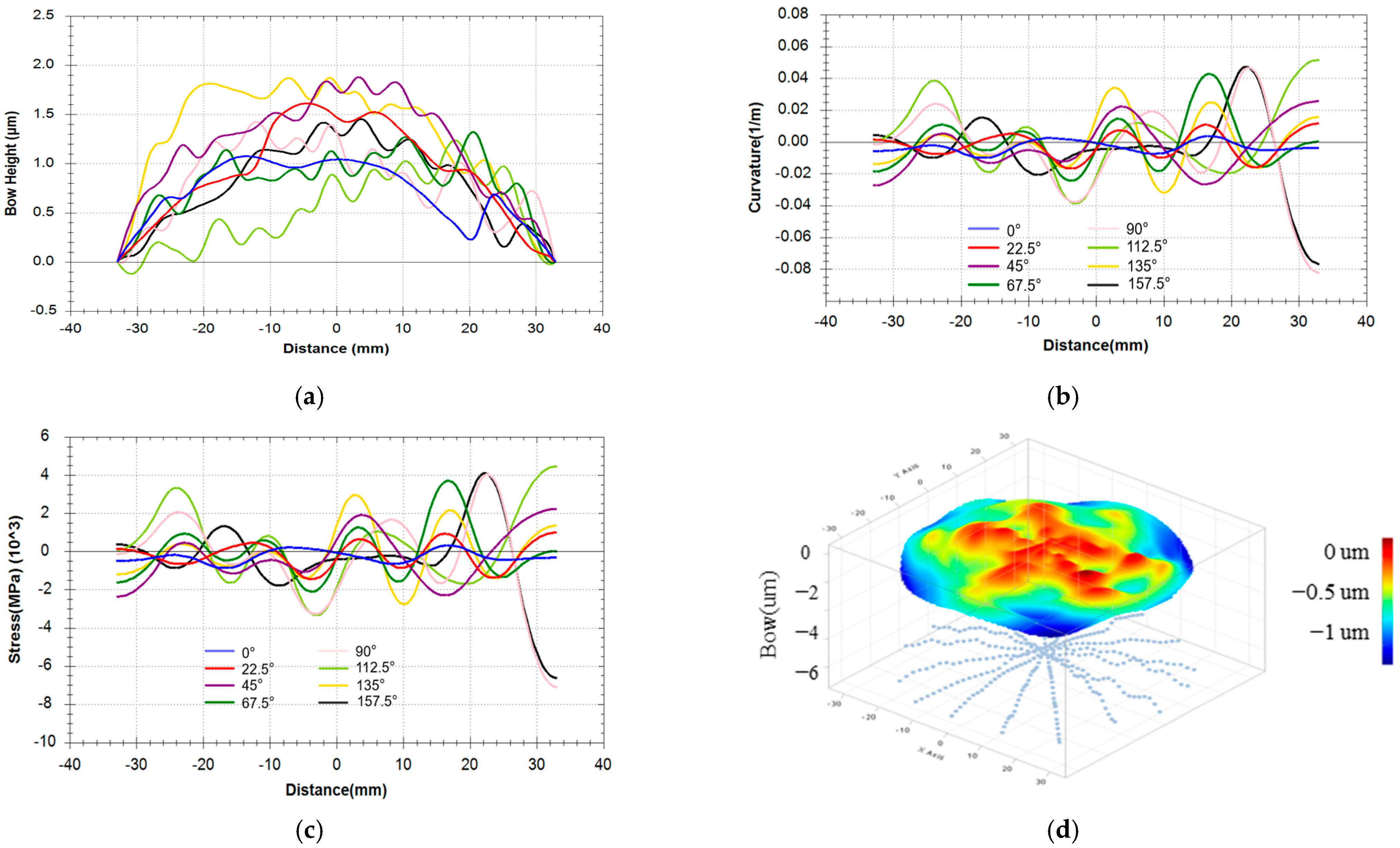
Firstly, the film stack structure is designed using two kinds of thin-film materials, namely Ti2O3 and SiO2, and through multiple optimizations, it is found that the film stress is hardly reduced to less than 50 MPa, and the film with a thickness of 400 nm to 900 nm designed with these materials is mostly positive stress. Therefore, it is considered to introduce a third kind of thin-film material with negative stress. It was found in the experiment that HfO2 film by electron beam evaporation is negative stress under appropriate process conditions, as shown in Figure 10. Moreover, the HfO2 film exhibits excellent optical performance, mechanical properties, and anti-laser damage performance in the visible-to-near-infrared band [16]. Therefore, the film stack structure is considered to be designed and optimized with three thin-film materials: Ti2O3, HfO2, and SiO2. According to the optimization goal of (16), the film stack structure is formed as S u b / 100 L / 3.31 M / 139.45 L / 13.14 M / 49.68 L / 30.89 H / 17.89 L / 77.12 H / 24.26 L / 24.59 H / 117.86 L / 4.45 H / 64.4 L / 108.72 M / 21.04 H / 98.17 L / A i r .
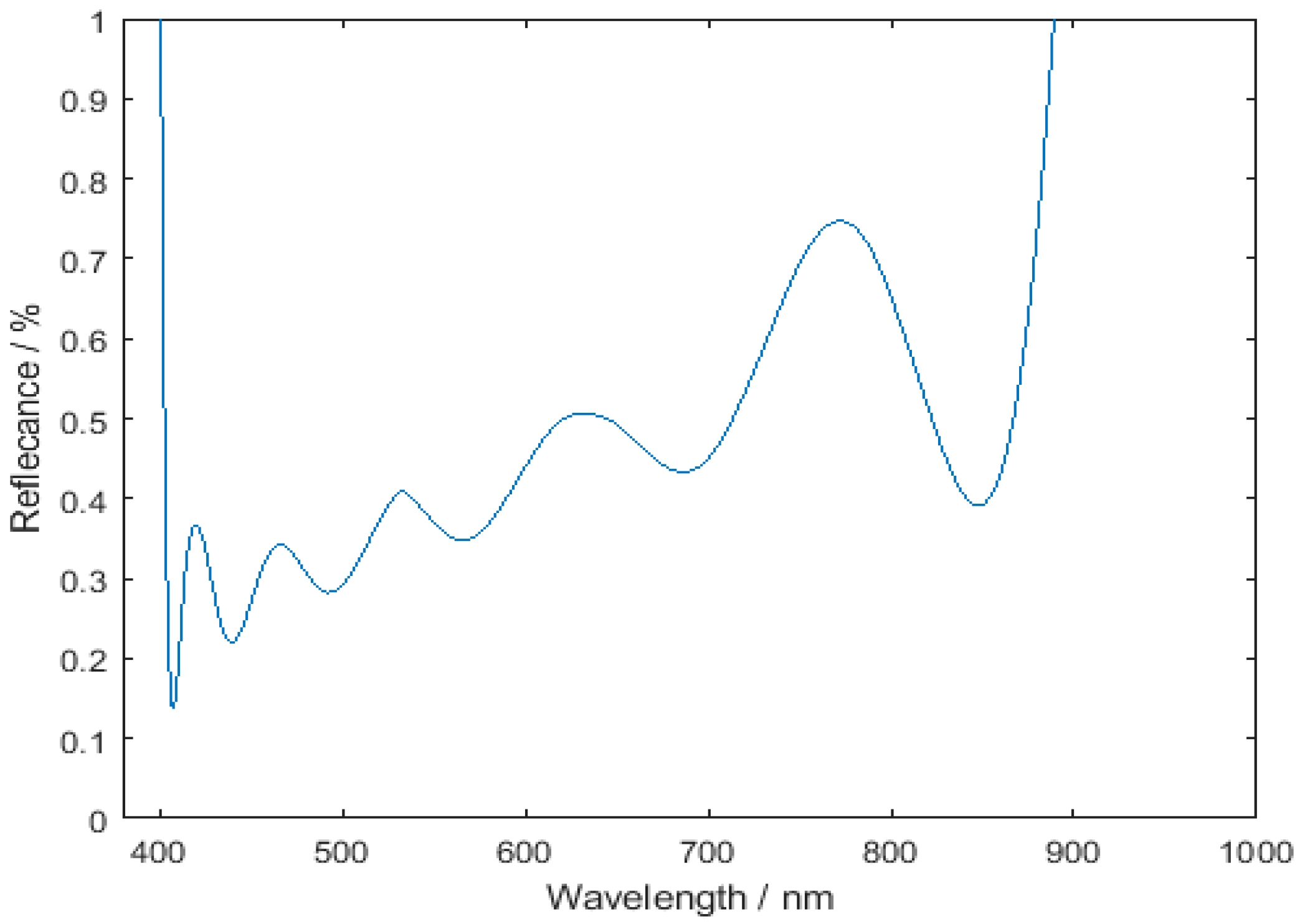
The spectral reflectance is shown in Figure 11. Where H, M, and L represent the Ti2O3, HfO2, and SiO2 films with an optical thickness of 111, respectively. The numbers in front represent the thickness, and the unit is nm. In the experiment, the stress test of the HfO2 film with a thickness of 100 nm was −235.67 MPa.
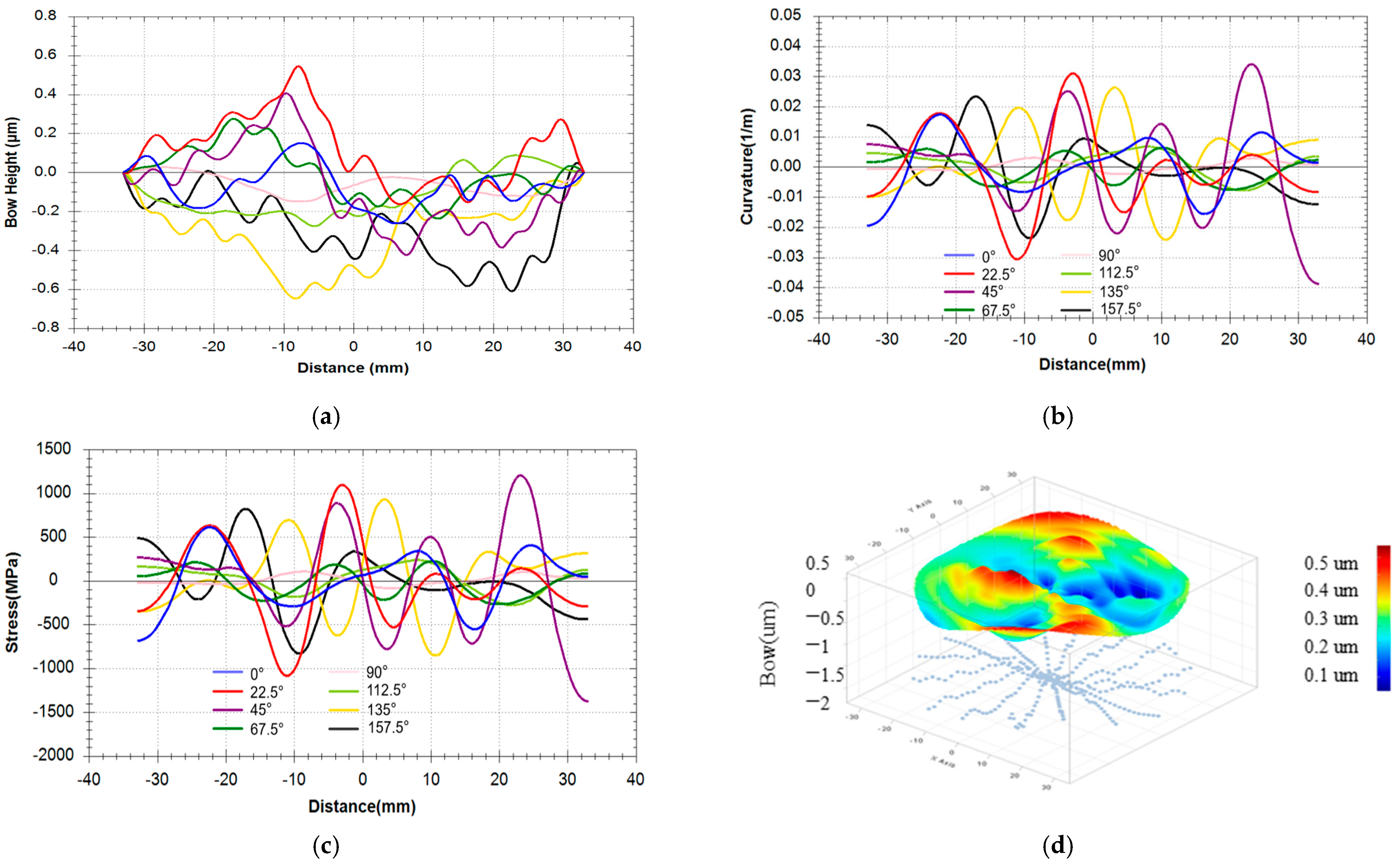
The total stress of the membrane structure is theoretically calculated as +25.45 MPa, and the remaining reflectivity is 0.48%, and the measured stress is +12.52 MPa, as shown in Figure 12.
The tested stress of the 16-layer film (antireflection film with a wide wavelength band of 400 nm to 900 nm) composed of three kinds of thin-film materials is 12.52 MPa. This result achieves the predetermined goal, but it has a large difference with the stress calculated by the theoretical model, and the relative deviation reaches 50%. The reason for this large relative deviation may be related to the excessive number of film layers and the variety of film materials. When the number of film layers is too large (for example, more than 10 layers), the density (refractive index) will cause changes to occur during the film deposition process [17,18,19]. In general, the density of most thin-film materials will decrease with the increase in the thickness and number of film layers. This phenomenon of thin-film density change will affect the accumulation of thin-film stress, resulting in a large deviation between the measured thin-film stress and the abovementioned theoretical model when the number of film layers is large and too thick, and the variety of materials is relatively large. In the designed 16-lyaer broadband antireflection film structure composed of three kinds of thin films, namely Ti2O3, HfO2, and SiO2, the first layer of thin film is SiO2, and its refractive index is very close to that of substrate K9. The thickness of the first layer of SiO2 thin film can be adjusted to appropriately change the size of the film structure stress, and this will not have too much of an effect on the spectral performance of the film structure. In any case, the design method mentioned in this study for eliminating the stress of the film has a certain application value and reference value the industry, and it can be used to simply and conveniently design and prepare the film under certain conditions.

4. Discussion

Based on Stoney’s film stress formula, this study established a mathematical model for calculating the stress of multilayer film systems and proposed a multi-objective optimization method integrating stress characteristics and spectral performance. Experimental results showed varying degrees of consistency between theoretical predictions and measurements, with distinct deviations in complex systems, which deserve in-depth analysis.
For ITO films with different thicknesses, the stress accumulation law conformed to theoretical expectations, with a deviation of approximately 6.6%, verifying the basic validity of the stress–thickness proportionality assumption. For the wide-angle (0°–55°) incident 1.064 μm laser and 3.7–4.8 μm mid-infrared dual-band antireflection coatings, the theoretical stress (70.424 MPa) and measured stress (74.61 MPa) showed a relative deviation of only ~2.9%, indicating that the model performs well for simple multilayer systems (six layers and two materials). However, for the 16-layer broadband antireflection film composed of Ti2O3, HfO2, and SiO2, the deviation between the measured stress (12.52 MPa) and theoretical calculation (25.45 MPa) reached nearly 50%, highlighting the model’s limitations in complex systems.
The main reasons for this deviation include the following. (1) Layer number effect: With 16 layers, the linear superposition assumption of the model is violated. Each new layer is deposited on a pre-stressed substrate/film system, causing partial relaxation of underlying stresses due to substrate bending or interlayer adhesion, a dynamic interaction not captured by the static model. (2) Material combination complexity: The three materials have distinct mechanical and thermal properties, leading to interfacial stress mismatches during deposition and cooling, generating additional stress components unaccounted for by simple superposition. (3) Changing film properties: For thick multilayers, film density (and refractive index) decreases with layer count, weakening intergranular interactions (Hoffman’s model) and reducing actual stress compared to single-layer data-based predictions. Residual gas adsorption or interdiffusion at interfaces further alters stress propagation.
Regarding stress distribution, the central area of samples showed better uniformity, which can be attributed to combined effects of thickness and substrate curvature. Subtle edge-to-center thickness gradients (0.1%–0.3%) from evaporator geometry induce localized stress differences, while symmetric stress accumulation in the center leads to more uniform bending, in contrast to enhanced curvature gradients at edges from asymmetric boundary effects. These insights guide process control, such as optimizing evaporator baffles or pre-calibrating substrate flatness.
Stress measurements relied on the FST5000 meter (based on substrate curvature and Stoney’s equation), which is effective for large-area average stress but can be complemented by XRD (for crystalline films), Raman spectroscopy (for amorphous films), nanoindentation (for mechanical property–stress correlations), and photoelasticimetry (for in situ stress evolution) to capture localized or dynamic stress features.
To improve the model for thicker/complex stacks, three modifications are proposed: (1) incorporating interfacial stress coefficients calibrated via XRD to account for heterointerfacial effects, (2) embedding dynamic functions for density and Young’s modulus to capture thickness-induced property variations, and (3) integrating finite element simulations to track real-time stress redistribution during sequential deposition.
Regarding practical applicability, strict control of deposition parameters ensured good repeatability (±3 MPa for six-layer films across three depositions). Preliminary 3-month observations under ambient conditions showed no significant stress variations (Δσ < 5 MPa) in dual-band coatings, indicating initial stability, though long-term tests under extreme conditions (thermal cycling and humidity aging) are planned.

5. Conclusions

This study established a mathematical model for calculating the stress of multilayer thin films based on Stoney’s formula and proposed a multi-objective optimization method integrating stress characteristics and spectral performance. Key conclusions are as follows:
(1)
The model accurately predicts stress in simple multilayer systems: for ITO films and six-layer dual-band antireflection coatings, test results matched theoretical calculations with deviations of ~6.6% and ~2.9%, respectively, verifying its effectiveness.
(2)
The model shows limitations in complex systems: for 16-layer broadband antireflection films with three materials, the stress deviation reached nearly 50%, mainly due to layer number effects, material mismatch, and evolving film properties during deposition.
(3)
Stress distribution uniformity is influenced by thickness gradients and substrate curvature, with better uniformity in the central area, providing guidance for process optimization (e.g., evaporator design and substrate flatness calibration).
(4)
Complementary characterization techniques (XRD, Raman, nanoindentation, and photoelasticimetry) can enhance stress measurement reliability, while model improvements (incorporating interfacial stress, adaptive parameters, and dynamic relaxation modeling) will extend its applicability to complex systems.
(5)
Good process repeatability and initial long-term stability indicate the method’s potential for practical applications, with further tests under extreme conditions planned to validate reliability.

Author Contributions

Conceptualization, S.W. and J.Z.; methodology, G.M.; validation, W.Y., S.W. and R.L.; formal analysis, Q.W.; investigation, S.W. and H.Z.; resources, Q.W.; data curation, W.Y.; writing—original draft preparation, S.W.; writing—review and editing, J.Z.; visualization, S.W.; supervision, W.W.; project administration, R.L.; funding acquisition, W.W. All authors have read and agreed to the published version of the manuscript.

Funding

This research was funded by Naval Systems Engineering Institute (China), grant number “X2313”.

Institutional Review Board Statement

Not applicable.

Informed Consent Statement

Not applicable.

Data Availability Statement

The raw data supporting the conclusions of this article will be made available by the authors on request.

Conflicts of Interest

The funders had no role in the design of the study; in the collection, analysis, or interpretation of data; in the writing of the manuscript; or in the decision to publish the results.

References

  1. Galib, M.; Orhan, O.K.; Liu, J.; Ponga, M. Residual stress development in lattice mismatched epitaxial thin films via atomic and molecular layer depositions. J. Mech. Phys. Solids 2024, 193, 105897. [Google Scholar] [CrossRef]
  2. Sun, Q.; Xie, F.; Zhu, M.; Wang, L.; Wang, D.; Wu, M. Analysis of stress corrosion craking failure of 316L stainless steel filow promoter string in the aggressive oilfield environment. Eng. Fail. Anal. 2025, 167, 109087. [Google Scholar] [CrossRef]
  3. Liu, B.; Shen, Z.; Li, X.; Kuang, D.; Liu, X.; Zhang, S.; Wen, C.; Zi, X.; Zhang, X.; Sun, H.; et al. Hydrogen behavior and microstructural evolution in flexible IGZO thin films under stress. Mater. Sci. Semicond. Process. 2025, 187, 109151. [Google Scholar] [CrossRef]
  4. Akatsu, T.; Inuzuka, H.; Shinoda, Y.; Wakai, F. Weight function for point-sharp nanoindentation to evaluate the mechanical properties of a film/coating on a substrate. Results Eng. 2024, 24, 103447. [Google Scholar] [CrossRef]
  5. Melnikova, S.D.; Larin, S.V. Mechanical properties of the multilayer polymer films: Molecular dynamics simulation. Comput. Mater. Sci. 2025, 247, 113545. [Google Scholar] [CrossRef]
  6. Jiang, J.; Jiang, L.; Cai, Z.; Wang, W.; Zhao, X.; Liu, Y.; Cao, Z. Numerical stress analysis of TBC-film cooling system under operating conditions considering the effects of thermal gradient and TGO growth. Surf. Cationg Technol. 2019, 357, 433–444. [Google Scholar] [CrossRef]
  7. Lablali, M.; Mes-Adi, H.; Mazroui, M. Effect of deposition rate and annealing on Nb thin film growth on Cu substrate: Molecular dynamics simulation. Vacuum 2024, 229, 113548. [Google Scholar] [CrossRef]
  8. Wang, J.; Ma, D.; Wang, L.; Liu, Y.; Lv, Y.; Tian, X.; Liang, L.; Xiao, W.; Gao, J. Thickness uniformity, electrical properties, and stress of sputtered TiN thin films. J. Phys. Conf. Ser. 2024, 2825, 012034. [Google Scholar] [CrossRef]
  9. Chen, S.X.; Chen, M.M.; Liu, Y.; Cao, D.W.; Chen, G.J. Interfacial stress engineering toward enhancement of ferroelectricity in Al doped HfO2 thin films. Chin. Phys. B 2024, 33, 098701. [Google Scholar] [CrossRef]
  10. Hsiao, S.-N. Oxidation-induced surface stress on texture development of thin films: The (001) FePt case. Vacuum 2024, 225, 1132788. [Google Scholar] [CrossRef]
  11. Tien, C.-L.; Chiang, C.-Y.; Wang, C.-C.; Lin, S.-C. Temperature-Dependent Residual Stresses and Thermal Expansion Coefficient of VO2 Thin Films. Inventions 2024, 3, 61. [Google Scholar] [CrossRef]
  12. Hoffman, R.W. Stress in thin films: The relevance of gain boundaries and impurities. Thin Solid Film. 1976, 34, 185–190. [Google Scholar] [CrossRef]
  13. Piombini, H.; Compoint, F.; Ambard, C.; Picart, D.; Belleville, P.; Damamme, G.; Brémand, F. Stress measurement of elastic sol-gel layer by photoelasticimetry—Comparison with Stoney. Mater. Express 2016, 6, 469–485. [Google Scholar] [CrossRef]
  14. Haw, M.T.X.; Lou, L.; Gu, Y.A. Effect of Stress on a Bimorph Piezoelectric Micromachined Ultrasound Transducer. In Proceedings of the 2015 IEEE International Conference on Electron Devices and Solid-State Circuits (EDSSC), Singapore, 1–4 June 2015; pp. 752–755. [Google Scholar]
  15. Sugiura, M.; Tamura, K.; Kobiyama, M. Quantitative calculation of substrate bending caused by multilayer coating stresses. Appl. Opt. 2020, 59, A92–A98. [Google Scholar] [CrossRef] [PubMed]
  16. Wang, B.; Zhang, J.; Liu, H.; Yang, H.; Wang, Y.; Wang, H.; Pan, J.; Liu, Z.; Shen, Z.; Gao, W.; et al. Effect of Ion-Assisted Deposition Energy of RF Source on Optical Properties, Microstructure, and Residual Stress of HfO2 Thin Films. Coatings 2024, 14, 14121616. [Google Scholar] [CrossRef]
  17. Xu, Z.-J.; Zhang, F.; Zhang, R.-J.; Yu, X.; Zhang, D.-X.; Wang, Z.-Y.; Zheng, Y.-X.; Wang, S.-Y.; Zhao, H.-B.; Chen, L.-Y. Thickness dependent optical properties of titanium oxide thin films. Appl. Phys. A 2013, 113, 557–562. [Google Scholar] [CrossRef]
  18. Golosov, D.A.; Vilya, N.; Zavadski, S.М.; Melnikov, S.N.; Avramchuk, A.V.; Grekhov; Kargin, N.I.; Komissarov, I.V. Influence of film thickness on the dielectric characteristics of hafnium oxide layers. Thin Solid Film 2019, 690, 137517. [Google Scholar] [CrossRef]
  19. Xu, Q.; Ma, Y.; Skowronski, M. Nanoscale density variations in sputtered amorphous TaOx functional layers in resistive switching devices. J. Appl. Phys. 2020, 127, 055107. [Google Scholar] [CrossRef]
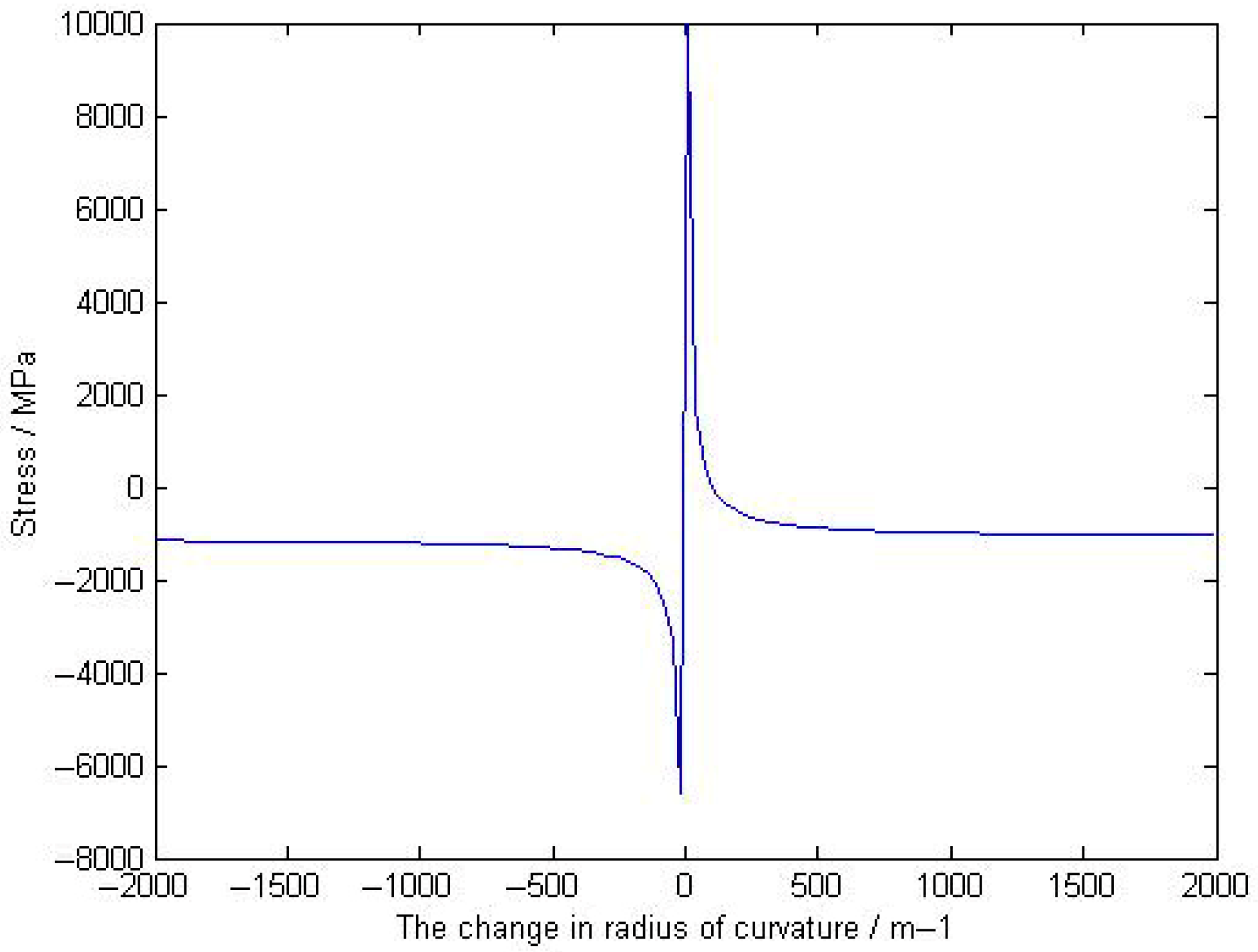
Figure 1. The amount of change in the radius of curvature caused by the film stress.
Coatings 15 00980 g001
Figure 2. Deformation of substrate curvature radius caused by thin-film stress: (a) before coating, (b) after single-layer coating, and (c) after multilayer coating.
Coatings 15 00980 g002
Figure 3. Diagram of stress-test scanning mode.
Coatings 15 00980 g003
Figure 4. Sample of ITO thin film coated on quartz wafer: (a) 1# ITO film sample and (b) 2# ITO film sample.
Coatings 15 00980 g004
Figure 5. Stress distribution in monolayer Ti2O3 and monolayer SiO2 films: (a) TiO3 single-layer sample, (b) SiO2 single-layer sample, (c) stress of single Ti2O3 film, and (d) stress of single SiO2 film.
Coatings 15 00980 g005
Figure 6. Thickness, stress accumulation, and reflectivity of the dual-band antireflection coating: (a) thickness of layers, (b) stress of layers, and (c) reflectance curve of dual-band antireflection film.
Coatings 15 00980 g006
Figure 7. Position–waist height curves and 3D morphologies of the samples before and after coating: (a) bow height before coating; (b) surface shape before coating; (c) bow height after coating; (d) surface shape after coating; (e) bow-height changes after coating and before coating; and (f) surface-shape changes after and before coating.
Coatings 15 00980 g007
Figure 8. Position-curvature curves of the samples before and after coating: (a) curvature before coating, (b) curvature after coating, and (c) curvature changes after coating and before coating.
Coatings 15 00980 g008
Figure 9. Stress distribution of wide-angle incident laser and mid-wave infrared dual-band film layers:: (a) the values of the stress test after coating, (b) the 3D map of the stress distribution.
Coatings 15 00980 g009
Figure 10. Stress condition of 100 nm thick HfO2 film deposited by electron beam evaporation: (a) the change in the bow height after coating; (b) the change in the curvature after coating; (c) the stress value after coating; (d) the 3D diagram of the stress distribution of the film.
Coatings 15 00980 g010
Figure 11. Remaining reflectivity of the antireflection film on the K9 substrate from 400 nm to 900 nm.
Coatings 15 00980 g011
Figure 12. Stress test situation of antireflection film on 400 nm–900 nm K9 substrate: (a) the change in the bow height after coating; (b) the change in the curvature after coating; (c) the stress value after coating; (d) the 3D diagram of the stress distribution of the film.
Coatings 15 00980 g012
Table 1. Parameters of ITO thin-film stress-test samples. Uncertain thickness of ±2 nm; uncertain stress value of ±5 MPa.
SamplesSubstrateΦ (mm) E s (GP) h s (mm) ν s R f (m) R s (m) h f (nm) σ (MPa)
1#Quartz3073.11.550.17198.5672.0120−527
2#Quartz3073.11.550.17−569.6389.6250−1171
Table 2. Thin-film stress-test parameters.
Substrate E s (GPa) h s (mm) ν s R f (m) R s (m)
Sapphire380 GPa0.5 mm0.28559.1 m406.2 m
Table 3. Single-layer film stress-test values. Uncertainty of thickness is ±2 nm, and uncertainty of stress value is ±2 MPa.
FilmsTi2O3Ti2O3SiO2SiO2
Thickness (nm)260350200300
Stress (MPa)−39.9−56.6+112.2+156.3
Table 4. Deposition process parameters of various thin-film materials.
FilmsDeposition RateAuxiliary Ion Source PowerO2 Flow RateBaking TemperatureBaking Temperature
Ti2O30.2 nm/s1.5 KW40 sccm2.0 × 10−6 mbar250 °C
SiO20.6–1.0 nm/s1.3 KW02.0 × 10−6 mbar250 °C
ITO0.4–0.7 nm/s1.3 KW30 sccm2.0 × 10−6 mbar280 °C
HfO20.2 nm/s1.8 KW40 sccm2.0 × 10−6 mbar250 °C
Disclaimer/Publisher’s Note: The statements, opinions and data contained in all publications are solely those of the individual author(s) and contributor(s) and not of MDPI and/or the editor(s). MDPI and/or the editor(s) disclaim responsibility for any injury to people or property resulting from any ideas, methods, instructions or products referred to in the content.