Article

Laser-Patterned and Photodeposition Ag-Functionalized TiO2 Grids on ITO Glass for Enhanced Photocatalytic Degradation

by
Bozhidar I. Stefanov
Department of Chemistry, Faculty of Electronic Engineering and Technologies, Technical University of Sofia, 8 Kliment Ohridski Blvd, 1756 Sofia, Bulgaria
Coatings 2025, 15(6), 709; https://doi.org/10.3390/coatings15060709
Submission received: 6 May 2025 / Revised: 6 June 2025 / Accepted: 10 June 2025 / Published: 12 June 2025
(This article belongs to the Special Issue Electrochemical Properties and Applications of Thin Films)

Abstract

Laser patterning of sol–gel-derived TiO2 coatings offers a promising route for fabricating TiO2-based devices. Conventional approaches require high-power CO2 lasers, whereas herein is demonstrated an alternative method using a low-cost, blue laser (λ = 445 nm, 1250 mW) to pattern TiO2 layers derived from a visible-light-absorbing titanium salicylate sol. Grid-shaped TiO2 patterns (~250 μm line, 500 μm pitch) were fabricated on indium tin oxide (ITO)-coated glass substrates via dip-coating, laser patterning, selective solvent removal, and annealing at 450 °C. Photocatalytic performance was enhanced through Ag photodeposition from a 5 mM Ag+ aqueous electrolyte under UV doses of 5, 10, and 20 J cm−2. Structural and compositional analysis (XRD, SEM-EDS, AFM, UV–Vis, Raman) confirmed the formation of crystalline anatase TiO2 and Ag incorporation proportional to the dose. Methylene blue (MB) photooxidation experiments revealed that Ag-functionalized samples showed up to 20% higher degradation efficiency and improved photocatalytic stability across eight consecutive MB oxidation cycles. Additional photoelectrochemical measurements confirmed the formation of a TiO2/Ag Schottky junction, while surface-enhanced Raman scattering (SERS) signals observed on Ag/TiO2 grids enabled the detection of MB adsorbates.

1. Introduction

Titanium dioxide (TiO2) is a transition metal oxide widely known for its photocatalytic properties. These arise from its excitation upon absorption of light energy greater than its bandgap (Eg = 3.2 eV for anatase TiO2, λ ≤ 388 nm), leading to the generation of electron–hole pairs. These excitons can migrate through the crystal lattice and initiate photooxidation or photoreduction reactions with chemical species adsorbed on the photocatalyst surface [1,2,3].
TiO2-based photocatalysts are extensively employed in a wide range of priority applications, such as environmental remediation technologies utilizing photoinitiated advanced oxidation processes for the complete mineralization of organic contaminants in polluted water and air [4,5,6]; energy conversion and storage devices such as solar-to-X systems [7,8,9,10]; and dye-sensitized solar cells (DSSCs) [11,12,13]. In many of these applications, TiO2 is used in the form of dispersed nanoparticles [7,10]; however, a more practical approach involves the use of supported TiO2-based structures—thin films and coatings [8,9], enabling reusable photocatalysts and thin-film devices [14,15].
The fabrication of TiO2-based thin-film devices commonly relies on advanced vacuum deposition methods such as RF and DC magnetron sputtering [16,17,18], electron beam evaporation [19], or chemical vapor deposition approaches like atomic layer deposition [20,21]. Nevertheless, flexible, low-cost wet-chemical deposition routes based on sol–gel formulations are widely adopted, particularly via simple dip-coating or spin-coating methods, which are popular within the photocatalytic thin-film research community [22,23,24].
A significant drawback of these solution-based deposition methods, however, is the difficulty in patterning TiO2 thin films, which is required for certain applications such as thin-film optoelectronic and memory devices [23,25]. While physical vapor deposition (PVD) films can be patterned using simple shadow masks or lift-off techniques [25,26,27], patterning sol–gel-deposited TiO2 often demands high-energy processing methods. These include vacuum UV irradiation to decompose acetylacetonate-based sols [28], focused electron beams [23], or the use of sensitizers like benzoylacetone to render the sol photosensitive [29,30].
A flexible, maskless method for direct patterning of TiO2 sols is laser processing, which decomposes the TiO2 sol into an insoluble or crystalline phase. However, this requires high-power deep-UV (KrF excimer) lasers [31] or far-infrared CO2 lasers [32,33], due to the poor light absorbance of most transparent TiO2 sols. Recently, the addition of noble metal nanoparticles has been shown to enhance laser absorption via thermoplasmonic effects. For instance, Noel et al. [34] demonstrated the use of gold nanoparticles to enable laser patterning of TiO2 sol using an NIR 808 nm laser.
An even more accessible approach was reported by Gerlein et al. [35], who demonstrated laser-assisted crystallization of an amorphous TiO2 precursor using a low-cost 405 nm laser. This was achieved using a colored amorphous TiO2 sol tailored for enhanced absorbance at the laser wavelength. In a previous study by the author of the present work, a strongly red–orange TiO2 deposition sol was developed based on a Ti–salicylate complex [36]. Its strong absorbance in the blue visible range makes it well-suited for laser patterning using inexpensive visible-light laser sources.
In addition, patterned TiO2 structures open up possibilities for their advanced functionalization via photodeposition. It is well-known that upon UV illumination, photocatalysts such as TiO2 can photoreduce noble or transition metal ions to their metallic form, enabling the direct deposition of reduced metal species onto the surface [27,37,38]. These may form Schottky-type barriers with TiO2, promoting electron transfer from the photogenerated excitons to the metal co-catalyst, thus suppressing charge recombination—a major source of photocatalytic efficiency loss [39,40]. Photodeposition tends to preferentially localize the metallic species on electron-rich defects, active sites, and facets with enhanced photoreduction activity [38,41] and allows fine-tuning of coverage by adjusting parameters such as UV dose.
Despite its potential, co-catalyst photodeposition on patterned TiO2 surfaces remains relatively unexplored. For example, Wu et al. selectively photodeposited Cu onto micropatterned TiO2 on a polymer dielectric substrate, showing that the reduced Cu species accumulated only on the TiO2 surface [28]. A promising but unexamined research direction is the study of photodeposition on patterned TiO2 layers deposited onto conductive oxides, such as indium tin oxide (ITO). It has been demonstrated that a heterojunction forms between TiO2 and ITO, enabling efficient electron transfer from TiO2 to the ITO substrate [42]. It is thus reasonable to expect that in patterned TiO2/ITO structures, the metal species may preferentially accumulate on the ITO regions. Furthermore, the surface topology of the TiO2 layer could potentially guide and localize metal photodeposition, as suggested in the work of Abshari et al. on gold deposition [27,43].
The aim of the present study is twofold: first, to demonstrate direct laser patterning of sol–gel-deposited TiO2 layers on ITO substrates using a cost-effective visible-light laser from a commercial laser engraver; and second, to investigate the photodeposition of a metal co-catalyst—namely, silver (Ag)—on these patterned TiO2/ITO surfaces. The effect of varied UV photodeposition doses on the photocatalytic and photoelectrochemical properties of the patterned layers will also be examined.

2. Materials and Methods

2.1. Materials and Reagents

ITO-coated glass substrates (50 mm × 50 mm × 1.1 mm, 135 nm thick ITO layer, ≤ 15 Ω sq−1) were procured from Saida Glass Co., Ltd. (Dongguan, Guangdong, China). Titanium (IV) isopropoxide (TTIP, 98+%), salicylic acid (SA, ACS, 99+%), silver nitrate (AgNO3, ACS, 99.9% metals basis), sodium sulfate decahydrate (Na2SO4·10H2O, 99+%, for analysis), methylene blue (95%), ethylenediaminetetraacetic acid disodium salt dihydrate (Na2EDTA·10H2O, 99+%), and dimethyl sulfoxide (DMSO, ACS, 99+%) were obtained from Thermo Scientific Chemicals (Waltham, MA, USA). Isopropyl alcohol (IPA, ≥99.8%, ChromAR, HPLC Grade) and acetone (ACS, 99.5+%) were supplied by Macron Fine Chemicals (Shanghai, China).

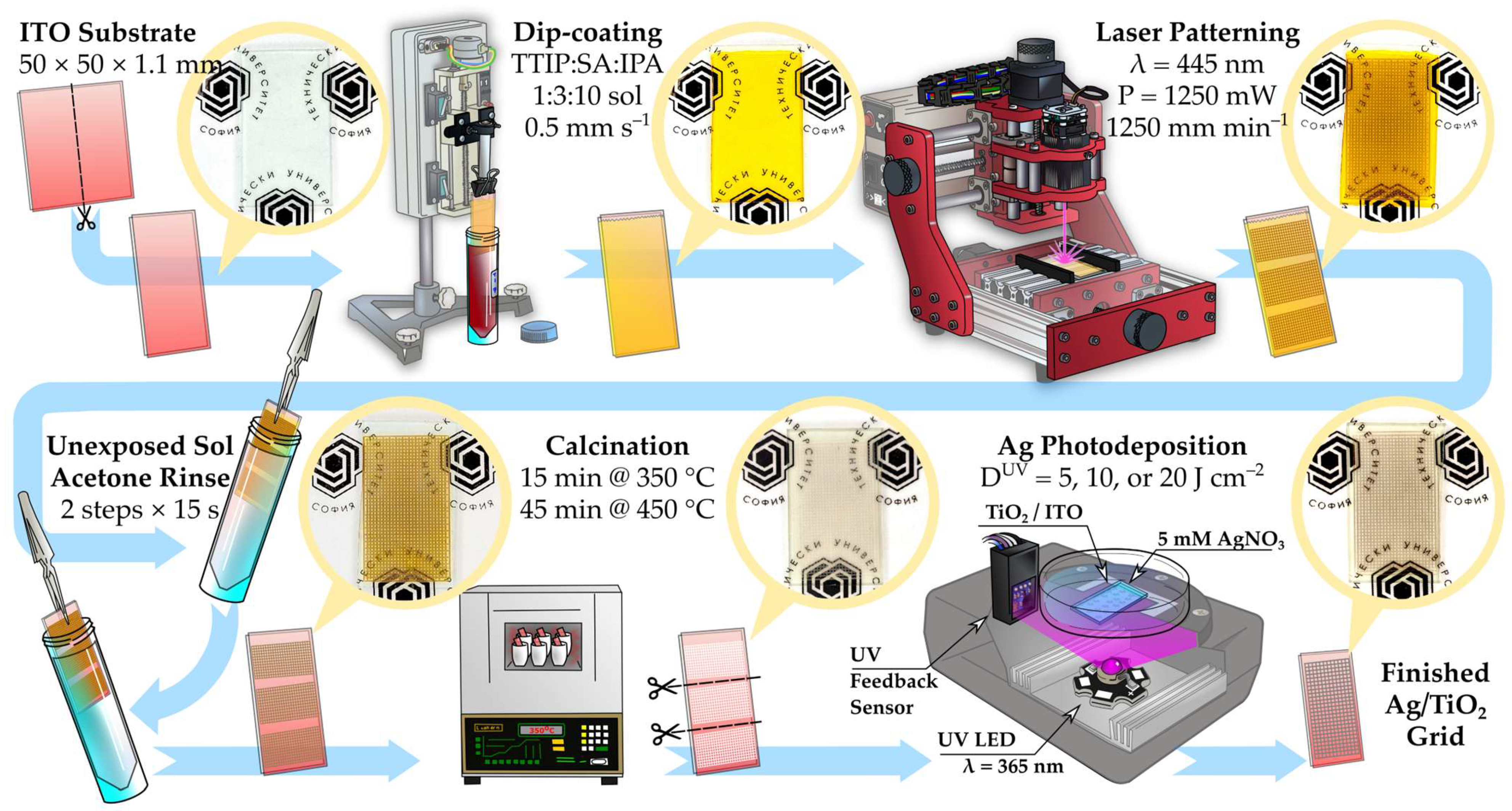
2.2. Fabrication and Ag Functionalization of Patterned TiO2 Layers

The technological steps for the fabrication and Ag photodeposition functionalization of the laser-patterned TiO2 grids on ITO-coated substrates are schematically illustrated in Figure 1. Each step is described in detail in the following subsections.

2.2.1. Sol–Gel Dip-Coating of the TiO2 Precursor Layer

The salicylate-based TiO2 deposition sol was prepared using a previously reported procedure [36]. Briefly, the sol consists of titanium (IV) isopropoxide (TTIP) as the Ti precursor, salicylic acid (SA) as a chelating agent to prevent TTIP hydrolysis by chelating the Ti(IV) ions, and isopropyl alcohol (IPA) as the solvent, in a 1:3:10 molar ratio. SA was first dissolved in IPA, followed by the dropwise addition of TTIP under magnetic stirring for 3 h. The resulting solution was a clear, intensely red–orange liquid due to the formation of the Ti[SA]3 complex. The sol was transferred into a sealed polypropylene container and aged for one week before use. It was found to remain stable for a year after preparation.
Dip-coating was performed using a custom-built, Arduino-controlled stepper motor-based apparatus. ITO-coated substrates were cut in half (25 mm × 50 mm × 1.1 mm) using a carbide glass cutter, cleaned by sonication in acetone for 3 min, and then dip-coated in a single cycle. The cycle consisted of immersion at 2.5 mm s−1, a 2 s dwell time, and withdrawal at 0.5 mm s−1. The coated substrates were left to dry for 5 min at ambient conditions, forming a uniform, intensely yellow sol layer (see Figure 1, top panel).

2.2.2. Laser Patterning of TiO2 Sol Layers

Two types of laser-patterned TiO2 substrates were prepared using the full area of the 25 mm × 50 mm × 1.1 mm sol-coated ITO substrates: either three 22.25 mm × 13.25 mm rectangles (for photocatalytic experiments) or two 18.75 mm × 18.75 mm squares (for photoelectrochemical measurements), each patterned with a 500 μm pitch square grid array in both x- and y-directions.
Laser patterning was carried out using a low-cost GRBL-based desktop CNC 1310 laser engraver/router equipped with a 445 nm laser diode (FB03 module, 2500 mW rated power; EleksMaker, Hong Kong, China). The dip-coated substrates were fixed on an aluminum holder on the laser bed and processed at 50% duty cycle PWM-modulated laser power and a feed rate of 1250 mm min−1. The optical power output under these conditions was measured as 1.1 W using a thermopile-based power density meter (PM400 with S175C thermal sensor, Thorlabs, Newton, NJ, USA). The estimated laser irradiation dose ( E ) was calculated as
E = P υ π r 2 ,
where P is the laser power (1.1 W), υ is the feed rate (21 mm s−1), and r is the beam radius (~0.125 mm), resulting in an estimated energy dose of approximately 1.1 J mm−2. Note that this is a rough estimate, as the laser beam quality is poor and reflections from the substrate and holder are not accounted for.
After laser patterning, the processed areas appeared visibly darker (see Figure 1). The unexposed sol was removed via a two-step acetone treatment: the sample was immersed in acetone for 15 s to dissolve the unprocessed sol, then transferred to a clean acetone bath, and finally dried with warm air. No yellow coloration remained, indicating complete removal of the unreacted sol. The patterned samples were annealed in a two-step program—15 min at 350 °C followed by 45 min at 450 °C—to ensure decomposition of organic residues and crystallization of the TiO2. After annealing, the individual grid arrays were separated by cutting with a carbide glass cutter and used for further processing.

2.2.3. Ag Photodeposition on TiO2 Grid Patterns

The TiO2 grid arrays were functionalized with silver via a UV-induced photodeposition process. A 5 mM aqueous AgNO3 solution served as the photodeposition electrolyte. A volume of 150 μL of this solution was placed in a 60 mm Petri dish, and the patterned TiO2/ITO substrate was positioned on top, with the TiO2-coated side facing downward, allowing the Ag+ solution to form a thin liquid film over the surface.
Photodeposition was carried out using an automated UV exposure setup described in detail in [44]. Briefly, the system features a high-power UVA LED source (KTDS-3534UV365B, λ = 365 ± 5 nm, 120° viewing angle, 620 mW radiant flux, Kingbright, Taipei, Taiwan) placed approximately 35 mm below the sample. Illumination intensity was monitored in situ by a calibrated ML8511 UV sensor (Lapis Semiconductor, Kanagawa, Japan), with feedback and integration handled by an Arduino microcontroller to deliver a specific UV dose ( D U V ).
Three photodeposition functionalization UV doses were applied: 5, 10, and 20 J cm−2, corresponding to exposure times of 543 ± 11 s, 1093 ± 11 s, and 2194 ± 35 s, respectively, yielding an average intensity ( I U V ) of 9.2 ± 0.2 mW cm−2. After photodeposition, the TiO2 patterns darkened visibly (see Figure 1). The samples were rinsed thoroughly with distilled water, dried with a heat gun, and used directly in photocatalytic and photoelectrochemical characterization without additional processing.

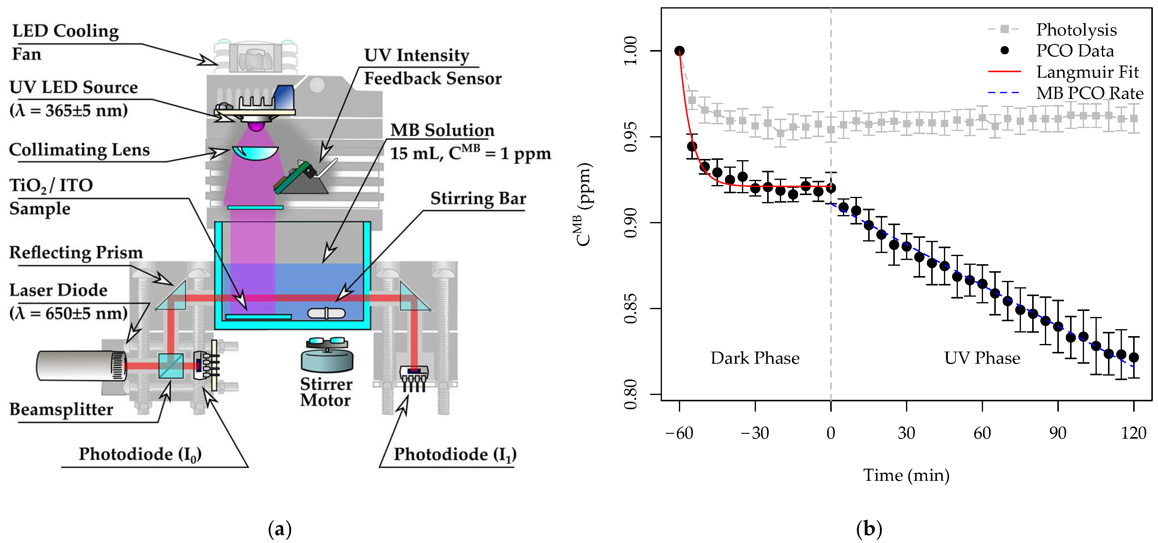
2.3. Methylene Blue Photocatalytic Oxidation Experiments

The photocatalytic activity of both pristine and Ag-functionalized TiO2 patterned grids was evaluated via aqueous-phase photocatalytic oxidation (PCO) of methylene blue (MB), a commonly used model contaminant. The experiments were conducted using a three-cell automated MB PCO activity screening reactor, equipped with an in situ MB colorimetry concentration monitoring system, thoroughly described and characterized in a previous publication [45].
Briefly, 15 mL of an aqueous MB solution with an initial concentration of C M B = 1 ppm was added to a 5 cm optical path-length glass cuvette (inner dimensions: 50 mm × 18 mm × 36 mm), which served as the reaction vessel. A TiO2-coated ITO sample (15 mm × 25 mm, with a 13.25 mm × 22.25 mm TiO2 grid-coated area) was placed inside the cuvette. Continuous stirring of the aqueous phase was ensured using magnetic agitation. A 3 W UVA LED light source (λ = 365 ± 5 nm, GP-3WUVA-G45, GMKJ LED, Shenzhen, China) was positioned above the sample to provide UV illumination. The output of the light source was monitored in situ by a UV intensity feedback sensor, similar to the one used in the photodeposition setup, and calibrated to reflect the UV irradiance ( I U V ) at the sample surface.
The MB concentration ( C M B ) was tracked in real time using an integrated laser colorimetry system (λ = 650 ± 5 nm), as illustrated in Figure 2a, which shows the cross-section of a single reaction cell. Laser intensity was measured before ( I 0 ) and after ( I 1 ) passing through the reaction cell using a pair of photodiode sensors. MB absorbance ( A M B ), which is proportional to the MB concentration, was calculated according to the following:
C M B A M B = log 10 ( I 1 / I 0 ) .
Each MB PCO experiment lasted a total of 180 min, starting with a 60 min dark phase (no UV illumination) to establish MB adsorption–desorption equilibrium, followed by 120 min of UV illumination. The UV intensity ( I U V ) at the TiO2 surface was estimated as 0.61 ± 0.06 mW cm−2. Concentration measurements were taken every 5 min to produce a C M B   vs. time profile, as shown in Figure 2b for a pristine TiO2/ITO patterned grid.
From the MB concentration profiles, two parameters were extracted. First, the MB equilibrium saturation coverage ( θ M B ) was estimated by applying a Langmuir adsorption isotherm to the dark-phase data using the following equation:
θ M B = ( 1 C M B ( t ) ) 1 exp k A d s M B t ,
where C M B t is the time-dependent MB concentration during the dark phase, k A d s M B is a fitting parameter representing the MB adsorption rate, and t is time.
Second, the MB photocatalytic oxidation rate ( k M B ) was obtained from the linear slope of the C M B decrease during the UV illumination phase. Both θ M B and k M B values were converted from ppm and ppm h−1 to nmol cm−2 and nmol cm−2 h−1 using the following equation:
[ n m o l ] = [ p p m ] × V × 10 12 M w M B × S ,
where V is the reaction volume (15 mL), M w M B is the molecular weight of MB (320 g mol−1), and S is the geometric area of the ITO substrate (1.5 cm × 2.5 cm = 3.75 cm2). The absolute substrate area was used to match the blank experiments, which employed uncoated ITO substrates of the same size.
The cycling stability of both pristine and Ag-functionalized TiO2/ITO patterned grids was evaluated over eight consecutive MB PCO cycles, each performed in triplicate. Between cycles, the samples were only rinsed with distilled water and air-dried.
Finally, blank experiments with uncoated ITO substrates were conducted to assess MB adsorption on the cell walls, stirring bar, and ITO surface.

2.4. Photoelectrochemical Measurements

The photoelectrochemical (PEC) activity of the samples was evaluated using a custom-built three-electrode PEC cell fabricated from PTFE. The internal dimensions of the cell were 20 mm × 20 mm × 10 mm. It was equipped with holders for two gasketed 25 mm × 25 mm side windows and a top opening for inserting the reference electrode. The working electrode was a TiO2/ITO sample (18.75 mm × 18.75 mm TiO2-coated area) mounted on one side, while the opposite side was fitted with a 1 mm thick optical glass window to allow light transmission. A 10 cm platinum wire, arranged in a cross configuration and positioned directly opposite the working electrode, served as the counter electrode. A 3.5 M Ag/AgCl electrode was used as the reference electrode. Illumination was provided by a UVA LED source (λ = 365 ± 5 nm), delivering a UV irradiance of 6.9 mW cm−2 at the surface of the working electrode. All measurements were carried out in a 0.5 M aqueous Na2SO4 electrolyte solution.
The potentials recorded against the Ag/AgCl reference electrode were converted to values versus the reversible hydrogen electrode (RHE) using the following equation:
E v s .   R H E = E v s .     A g / A g C l + 0.059 p H + E ° A g / A g C l ,
where E v s .   A g / A g C l is the measured potential, the electrolyte pH was 7.6, and the standard electrode potential for Ag/AgCl E ° A g / A g C l is 0.205 V vs. NHE.
All PEC measurements were performed using a PalmSens4 potentiostat/galvanostat/impedance analyzer (PalmSens BV, Houten, The Netherlands). Linear sweep voltammetry (LSV) was conducted over a potential range of −0.25 to 1.5 V vs. RHE, with a sweep rate of 5 mV s−1. Chronoamperometric photocurrent measurements were performed at a fixed potential of 1.23 V vs. RHE under pulsed UV illumination, with each illumination period lasting 60 s. Two types of electrochemical impedance spectroscopy (EIS) measurements were carried out under two sets of conditions. First, measurements were conducted at open circuit potential (OCP), with a frequency sweep from 100 kHz to 10 mHz, for subsequent Nyquist and Bode plots. Second, EIS was performed as part of a Mott–Schottky analysis by applying a potential sweep from −0.25 to −1.0 V vs. RHE in 25 mV increments, with impedance data recorded at fixed frequencies of 500, 1000, 1500, and 2000 Hz.

2.5. Characterization Techniques and Data Analysis Tools

UV/Vis transmittance spectra were recorded using a SP-V1100 spectrophotometer (DLAB Scientific Co., Ltd., Beijing, China). Laser emission spectra were obtained with an Oriel 77400 spectrograph (Newport, Irvine, CA, USA), equipped with a 400 lines mm−1 diffraction grating, a 1 mm slit, and a 2048-pixel CCD sensor. FTIR spectra were measured using a Cary 630 spectrometer (Agilent Technologies Inc., Santa Clara, CA, USA), equipped with a Diamond-ATR (Attenuated Total Reflectance) accessory.
X-ray diffraction (XRD) patterns were acquired on a Bruker D8 Advance diffractometer (Bruker AXS GmbH, Karlsruhe, Germany), using a Cu Kα radiation source and a LynxEye detector. Raman spectra were collected using a TO-ERS-532 spectrometer (Thunder Optics S.A.S., Montpellier, France) with a 532 nm laser (30 mW optical power) and a Raman probe equipped with a 20× microscope objective. The integration time for Raman measurements was set to 2500 ms.
Scanning electron microscopy (SEM) was performed using a Lyra I XMU microscope (TESCAN Group, Brno, Czech Republic). Elemental analysis via energy-dispersive X-ray spectroscopy (EDS) was conducted using a Bruker Quantax 200 detector (Bruker Nano GmbH, Berlin, Germany).
The sol viscosity was measured using a SNB-2T rotary viscometer (Dongguan Lonroy Equipment Co., Ltd., Dongguan, China) equipped with a stainless steel 0# L rotor. Optical micrographs at 100× magnification were acquired using an IM-3MET metallographic microscope coupled with a C-B10+ 10 MP CMOS camera (Optika S.r.l., Ponteranica, Bergamo, Italy). Atomic force microscopy (AFM) was performed on a Dimension 3100S-1 AFM system (Veeco Instruments Inc., Plainview, NY, USA) operated in tapping mode, using a Tap300Al-G AFM probe (BudgetSensors, Innovative Solutions Bulgaria Ltd., Sofia, Bulgaria). AFM data were processed using Gwyddion software (v.2.68, Czech Metrology Institute, Brno, Czechia). Electrochemical data acquisition and impedance fitting were performed using PSTrace 5 software (v. 5.9.2317). General data processing and figure plotting were carried out in R (version 4.4.0, 24 April 2024), and artwork was created using Inkscape (v.1.3.2).

3. Results and Discussion

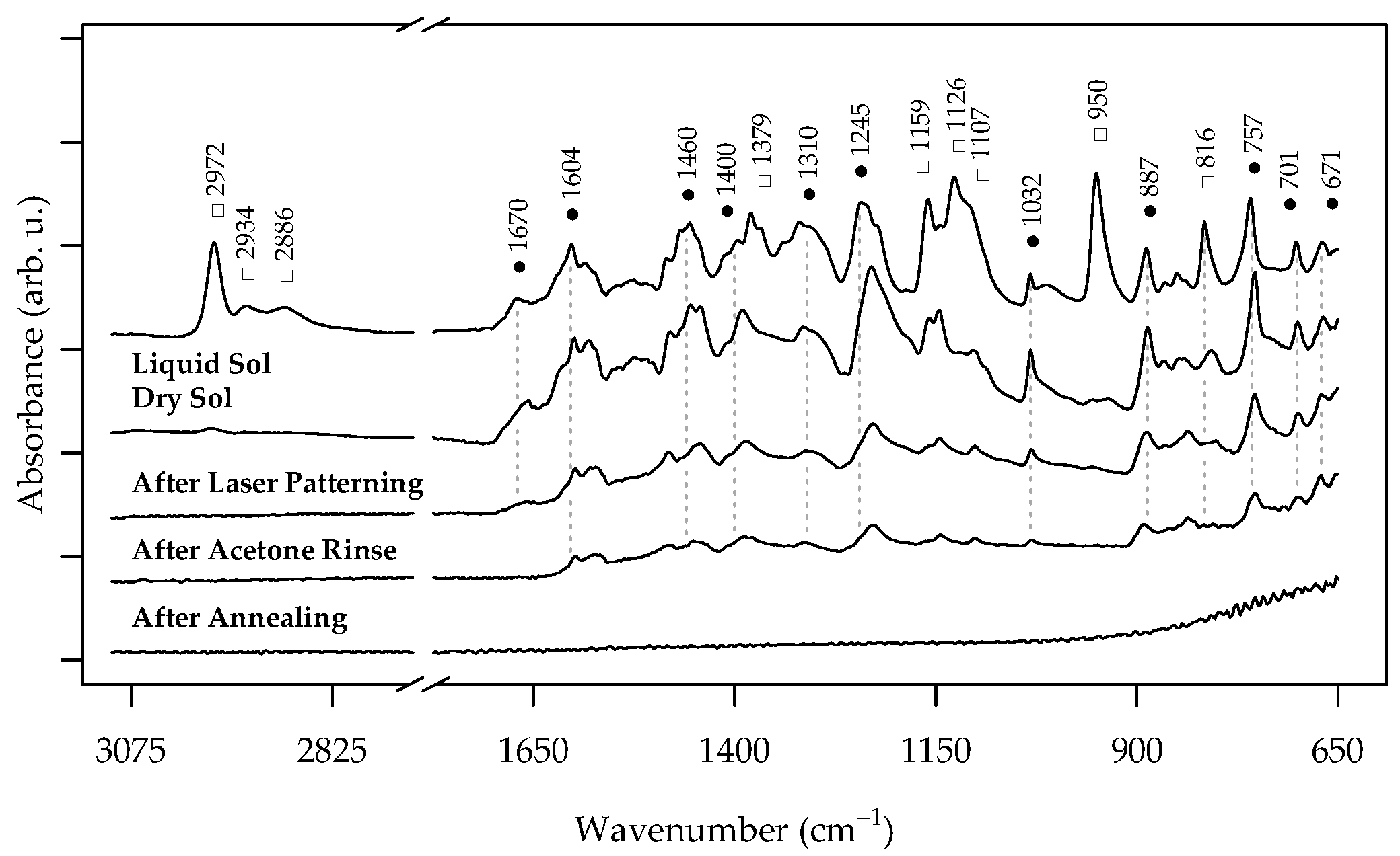
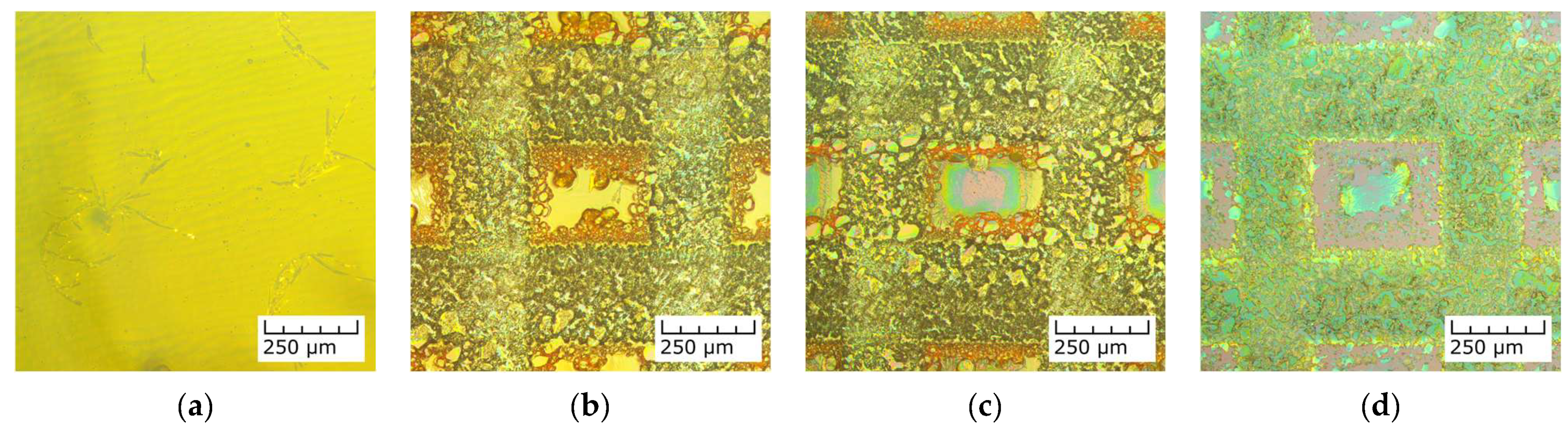
3.1. Laser Interaction with the Salycilate TiO2 Sol Dip-Coated Layers

As shown in the photographic insets in Figure 1, laser patterning of the salicylate-based TiO2 precursor sol clearly induces observable changes, indicating that sufficient light energy is absorbed by the sol during processing. To verify whether the absorbance of the sol layer is adequate in the spectral region corresponding to the 445 nm laser diode emission, UV-Vis transmittance spectra of the dip-coated sol layer on an ITO substrate were measured. Figure 3 presents a comparison between the UV-Vis spectrum of the sol layer and the emission spectrum of the laser. The laser was found to emit at a central wavelength of 445.1 nm with a broad full width at half maximum (FWHM) of 24.2 nm, which is typical for low-cost, high-power commercial laser diodes.
The dip-coated TiO2 sol layer exhibited an intense yellow coloration, and as shown in Figure 3, it displayed strong light absorption below 500 nm, with transmittance dropping to just 0.57% at 445 nm—demonstrating strong spectral overlap with the laser emission. For comparison, the bare ITO substrate, whose transmittance spectrum is also included in Figure 3, exhibited high transparency with transmittance exceeding 80% in the same spectral range. This suggests that minimal laser-induced damage is expected for the underlying ITO layer during patterning.
The development of the TiO2 sol layer thickness was further analyzed based on its UV-Vis spectrum (Figure 3). The transparent region above λ > 500 nm exhibits well-defined interference fringes, whose positions (indicated in Figure 3) can be used to estimate the thickness of the dip-coated sol layer. According to the well-established relation for thin-film interference, the thickness ( d ) can be estimated as follows:
d = λ λ 2 n ( λ λ ) ,
where λ and λ   are the wavelengths of any two adjacent interference maxima or minima (with λ > λ ) and n is the refractive index of the thin film [46,47]. Assuming a mean refractive index of n = 1.52, between that of TTIP (1.46) and salicylic acid (1.58), and applying Equation (6) to the five interference maxima identified in Figure 3, the calculated average dry sol layer thickness is 2.56 ± 0.06 μm.
The physicochemical properties of the salicylate sol were also characterized: its density ( ρ ) was determined gravimetrically as 0.965 ± 0.009 g cm−3, viscosity ( η ) was measured via rotary viscometry as 15.3 ± 0.1 mPa·s, and surface tension ( σ ) was determined as 27.3 ± 0.4 mN m−1 using stalagmometry, based on the drop weight method. Surface tension was calculated relative to isopropanol (IPA, σ I P A = 20.9 mN m−1 [48]), using σ s o l = σ I P A ( m s o l / m I P A ) , where m s o l and m I P A are the average drop masses of the sol and IPA, respectively [49]. All measurements were performed at the ambient temperature during dip-coating (18.9 °C).
Using these parameters, the thickness of the deposited liquid sol layer was estimated via the Landau–Levich–Derjaguin (LLD) model [50,51]:
d L L D = 0.945 σ ρ g η U σ 2 / 3     ,
where U = 0.5 mm s−1 is the withdrawal rate and g = 9.8 m s−2 is gravitational acceleration. The predicted wet layer thickness was 6.88 ± 0.06 μm.
Assuming complete evaporation of the IPA solvent, the expected dry layer thickness can be estimated by scaling the LLD value with the volumetric fraction of the Ti[SA]3 complex in the sol:
ϕ T i S A 3 = V T T I P + V S A V s o l   ,
where V T T I P , V S A , and V s o l are the volumes of TTIP, salicylic acid, and the total sol, respectively. Based on sol stoichiometry and the known densities of these components, ϕ T i S A 3 was estimated as 0.434. Applying this factor gives a predicted dry layer thickness of 2.99 ± 0.03 μm—reasonably close to the 2.56 ± 0.06 μm value obtained from UV-Vis interference analysis. The slight deviation may be due to the assumption of ideal volume additivity in the Ti[SA]3 complex formation.
As a final verification, the mass-per-area loading of the dry film ( Δ m d r y ) was estimated using the following:
Δ m T i S A 3 = d L L D ρ s o l ( m T T I P + m S A ) ( m T T I P + m S A + m I P A )   ,
where m T T I P , m S A , and m I P A are the respective masses of the sol components. This calculation yields a theoretical film loading of 383 ± 3 μg cm−2.
Experimentally, this value was validated by weighing a set of three glass slides before and after dip-coating using an analytical balance (0.01 mg readability). The average mass increase was 10.22 ± 0.55 mg, and when normalized to the coated area (~27 cm2), yielded 376 ± 9 μg cm−2, in excellent agreement with the theoretical estimate. These results confirm that the dry sol layer has a thickness in the 2.5–3.0 μm range and that complete solvent evaporation occurred.
To investigate the chemical changes occurring in the salicylate TiO2 sol layer during the laser patterning and post-processing steps, ATR-FTIR spectra were recorded after each key stage. A comparison of these spectra with that of the liquid deposition sol is presented in Figure 4.
The liquid salicylate sol exhibits a complex ATR-FTIR spectrum, which was thoroughly analyzed and computationally modeled in a previous publication [36] to confirm the presence of the Ti[SA]3 complex. Key spectral features include absorption bands at 1670, 1604, 1400, and 1310 cm−1, attributed to the ν(C=O), asymmetric and symmetric ν(COO), and δ(OH) modes of the salicylic acid carboxylic group. Additional peaks at 1460 and 1032 cm−1 are associated with aromatic ν(C=C) and δ(C=C) ring modes, while the band at 1245 cm−1 corresponds to the phenolic ν(Ph–OH) stretch. Bands at 757 and 701 cm−1 are due to out-of-plane δ(C=C) and δ(CH) bending vibrations, and peaks at 887 and 671 cm−1 are associated with ν(Ti–O) stretching vibrations.
The spectrum also contains several bands associated with the IPA solvent, including a peak at 1379 cm−1, a triplet from 1159 to 1107 cm−1, peaks at 950 and 816 cm−1, and a characteristic alkyl stretching triplet in the 2972–2886 cm−1 region. Notably, in the ATR-FTIR spectrum of the dip-coated but unprocessed sol layer, all IPA-related bands are nearly absent, indicating successful solvent evaporation. In contrast, the spectral features associated with the Ti[SA]3 complex remain intact, confirming the high stability of the SA-chelated Ti(IV) complex.
Following laser patterning, and particularly after acetone rinsing to remove unexposed sol, the Ti[SA]3-associated bands are significantly diminished, indicating decomposition or removal of the complex. After thermal annealing at 450 °C, no trace of organic residues is detectable by ATR-FTIR, confirming that the sol has been fully mineralized into an inorganic TiO2 phase.
The microstructural evolution of the laser-patterned salicylate-based TiO2 sol surface was also examined using optical microscopy. A series of 100× magnification micrographs is presented in Figure 5.
The as-deposited dry sol layer (Figure 5a) exhibits a uniform morphology, along with the appearance of some needle-shaped crystalline inclusions, which may correspond to crystallized excess salicylic acid (SA). In the laser-patterned layer (Figure 5b), the processed tracks appear visibly darker and exhibit a distinct “orange peel” texture, composed of alternating rough, island-like regions and smoother flat zones. This morphology is attributed to localized contraction during thermal decomposition of the precursor and is consistent with observations reported by Colusso et al. [52] and Matsubayashi et al. [53] for laser-treated sol–gel films. The unexposed central square areas within the grid remain mostly unaffected by the laser, though minor foaming is occasionally visible near their edges.
After the acetone rinse step (Figure 5c), the removal of unpatterned TiO2 sol becomes evident by the loss of yellow coloration and increased visibility of the underlying ITO layer, which appears reddish under reflected light. However, some residual sol is still visible, particularly in the central regions of the unexposed grid squares, suggesting that mechanical agitation during rinsing may improve sol removal.
Following the final annealing step (Figure 5d), the transformation of the laser-processed Ti[SA]3 sol into an oxide phase is clearly evident. The preserved “orange peel” morphology—consisting of rough islands embedded in a smoother continuous matrix—remains visible, highlighted by optical interference contrast. The untreated regions reveal a clear view of the ITO substrate, although remnants of unremoved sol persist in some central areas, indicating incomplete dissolution.

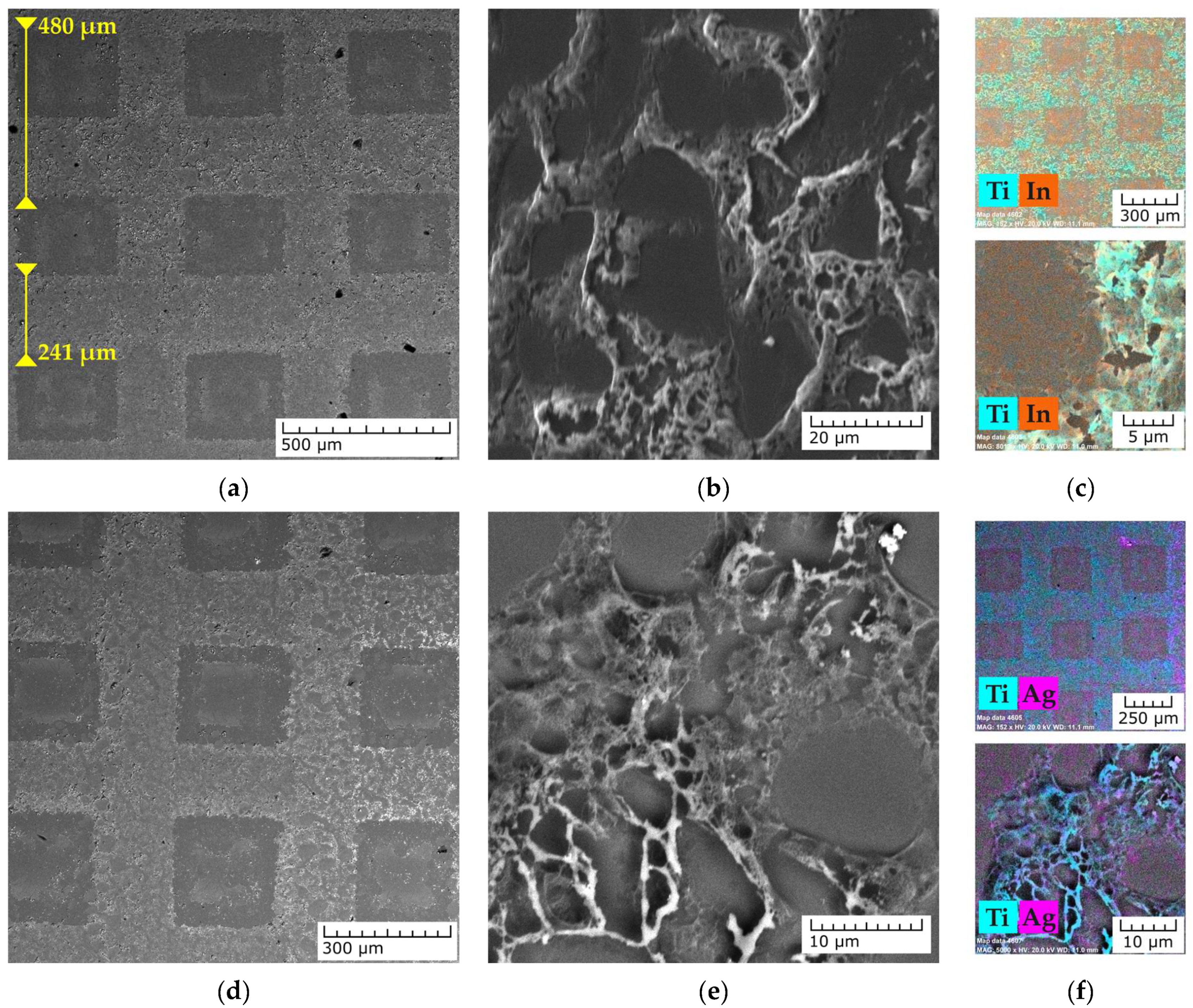
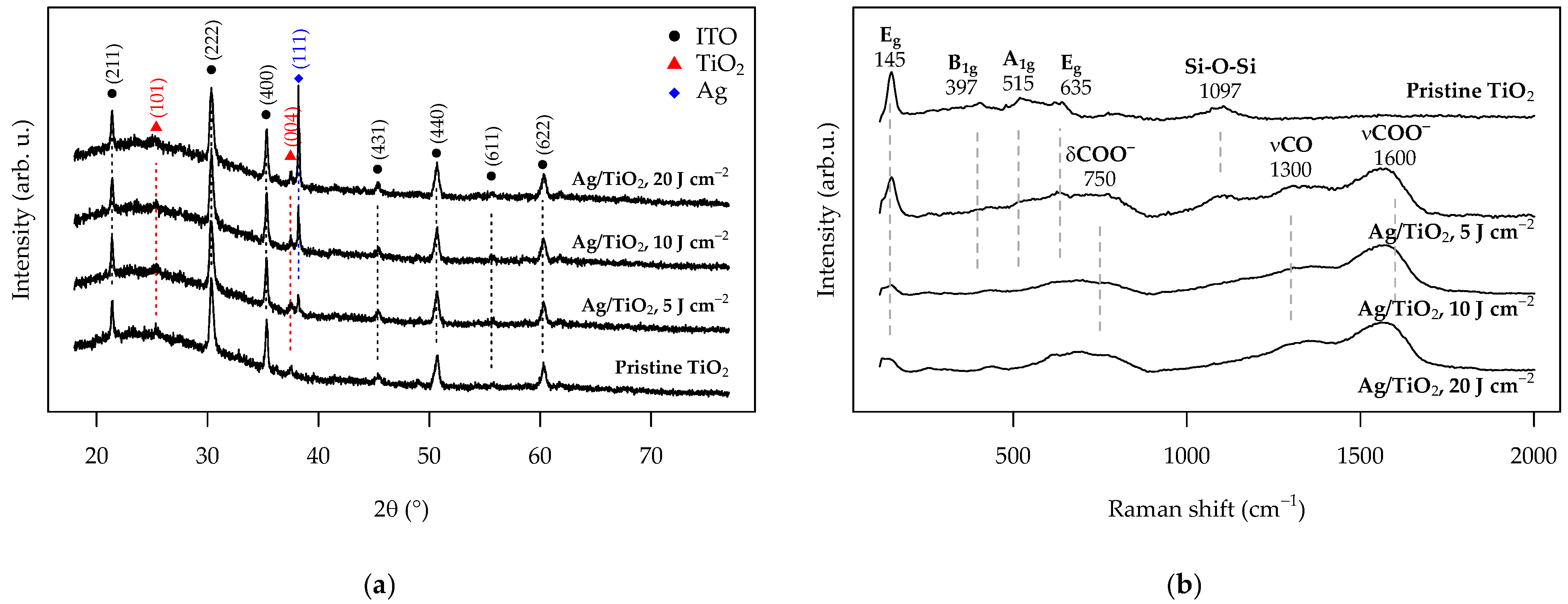
3.2. Characterization of the Pristine and Ag-Functionalized TiO2 Grid Patterns

The morphology of the laser-patterned pristine and Ag-functionalized TiO2 grid samples was investigated using scanning electron microscopy (SEM) and energy-dispersive X-ray spectroscopy (EDS) mapping. The resulting micrographs are presented in Figure 6. In the case of the pristine TiO2 sample (Figure 6a), the laser-patterned grid is clearly visible. The measured pitch of the mesh was 480 μm, which represents a 5% deviation from the intended 500 μm—indicating that the low-cost desktop engraving system provided sufficient patterning precision.
The patterned line width was found to be approximately 240 μm in the y-direction and 200 μm in the x-direction, with an average of 217 ± 19 μm based on multiple measurements. This anisotropy is attributed to the imperfect beam profile of the low-cost laser diode. Figure 6b shows a higher-magnification view of the TiO2 trace, revealing a porous morphology with ganglia-like inclusions and surface undulations on the order of ~1 μm, embedded within a smoother, denser underlying layer. This morphology is consistent with previous reports using similar laser engraving setups to pattern TiO2 films [35].
Elemental mapping via EDS (Figure 6c) confirmed the distribution of titanium within the grid lines. The two inset images show a top-down view of the patterned surface and the edge between the TiO2-coated and uncoated ITO regions. Both demonstrate a sharp boundary in Ti-Kα signal intensity, confirming good lateral confinement of the TiO2 phase within the laser-processed lines. However, some residual material was visible in the central areas of the mesh squares—likely due to incomplete removal of the unexposed sol during the acetone rinsing step.
For the Ag-functionalized samples, a representative set of images for the sample processed at a UV dose D U V of 20 J cm−2 is shown in Figure 6d–f. After Ag photodeposition, increased contrast was observed across the TiO2 grid in the SEM images (Figure 6d), likely due to enhanced backscattering from the silver phase. At higher magnification (Figure 6e), no major changes in the TiO2 line morphology or formation of large Ag particles or crystalline features were detected. However, EDS mapping (Figure 6f) revealed a relatively uniform Ag distribution, with the strongest Ag signals located near Ti-rich inclusions. This suggests that Ag was photodeposited preferentially in proximity to the TiO2 features, possibly forming a thin, conformal layer on the ITO surface.
The atomic Ag content increased with the applied UV dose, from 0.12 at.% at 5 J cm−2 to 0.13 and 0.16 at.% at 10 and 20 J cm−2, respectively. This corresponds to an Ag/Ti ratio of 3.6–5.6% when normalized to the detectable Ti signal.
To obtain additional surface-sensitive insight into the morphology of the patterned TiO2 surfaces, atomic force microscopy (AFM) topography images were recorded for both pristine TiO2 and Ag-functionalized TiO2 grids. The set of AFM scans, presented in Figure 7, was collected from three distinct regions identified based on morphological differences observed in both optical (Figure 5) and SEM images (Figure 6): (i) the uncoated ITO areas near the center of the grid squares (Figure 7a–d); (ii) the flat regions within the laser-treated TiO2 grid lines (Figure 7e–h); and (iii) the rougher, island-like areas embedded within the grid lines (Figure 7i–l).
Starting with the bare ITO substrate areas (Figure 7a–d), the typical morphology of PVD-deposited ITO is observed, consisting of globular particles and a cauliflower-like texture [54]. No morphological differences were evident between the pristine and Ag-functionalized samples in these uncoated regions.
In the laser-patterned TiO2 regions, the flat inland spots (Figure 7e–h) displayed a much smoother surface, especially in the Ag-functionalized samples (Figure 7f,h). Pores of varying size were present in some cases (notably in Figure 7e,g), which may result from localized bubbling during laser treatment. The average coating thickness in these flat regions was estimated at approximately 50 nm. However, Ag photodeposition did not significantly alter the morphology in these flat areas.
A notable distinction was observed in the rougher island regions within the patterned grid lines (Figure 7i–l). In the pristine TiO2 sample (Figure 7i), the islands consisted of densely packed round features, 20–100 nm in diameter, forming a wrinkled morphology. In contrast, Ag-functionalized samples (Figure 7j–l) exhibited surface coverage by flat, sheet-like particles with angular geometric shapes. This morphology is consistent with structures previously reported for silver photodeposition from aqueous media [55], indicating the successful deposition of Ag onto the TiO2 islands.
To investigate the phase composition of the TiO2 and photodeposited Ag, X-ray diffraction (XRD) patterns were recorded and are shown in Figure 8a.
The diffraction patterns were dominated by peaks corresponding to the ITO substrate, located at 21.4°, 30.4°, 35.3°, 50.7°, and 60.2° 2θ, which correspond to the (211), (222), (400), (440), and (622) planes of ITO (PDF 01-089-4597). In addition, reflections from anatase TiO2—most notably the (101) and (004) planes—were also observed (PDF 03-065-5714). The relatively strong intensity of the (004) peak suggests preferential texturing of the TiO2 phase. Scherrer analysis of this reflection yielded a mean crystallite size of approximately 34 nm.
Interestingly, while Ag particles were not clearly distinguishable in SEM micrographs, XRD revealed a distinct peak at 38.2° 2θ, corresponding to the (111) reflection of metallic silver (PDF 00-002-1098). The intensity of this peak increased with the applied UV dose, indicating a dose-dependent accumulation of the Ag phase. The mean Ag crystallite size, as estimated from Scherrer analysis, was 43 nm for samples treated at 5 and 10 J cm−2, increasing slightly to 49 nm at 20 J cm−2.
Raman spectroscopy (Figure 8b) further confirmed the anatase phase of the laser-processed TiO2, with characteristic vibrational bands observed at 145 and 635 cm−1 (Eg modes), and at 397 and 515 cm−1 (B1g and A1g modes), consistent with literature values [56]. A broad band at 1097 cm−1 was also present, corresponding to Si–O–Si stretching vibrations from the glass substrate [57].
In the Ag-functionalized samples, several changes were evident in the Raman spectra. The anatase vibrational bands appeared broader and less intense with increasing D U V , consistent with earlier reports of surface stress effects induced by strong interactions between photodeposited metals and TiO2 [44,58,59]. Additionally, broad features emerged at 750, 1300, and 1600 cm−1 in the Ag-functionalized samples, and their intensity increased with higher D U V . These bands are likely attributable to δ(COO), ν(CO), and ν(COO) modes of surface-adsorbed carbonates, potentially originating from atmospheric CO2 adsorption. Similar features have been observed in the Raman spectra of dispersed Ag phases [60,61] and may suggest surface-enhanced Raman scattering (SERS) effects.

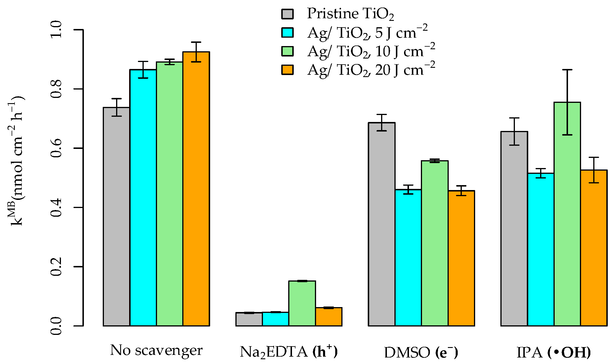
3.3. Photocatalytic Activity of the Pristine and Ag-Functionalized TiO2 Grid Patterns

The photocatalytic activity of the patterned pristine TiO2 and Ag-functionalized TiO2/ITO samples was evaluated through methylene blue (MB) adsorption and photocatalytic oxidation (PCO) experiments. Results are presented in Figure 9. All experiments were performed in triplicate, with each sample undergoing a total of eight consecutive MB PCO cycles.
The dark-phase adsorption isotherms from the first MB PCO cycle, used to determine the saturation coverage ( θ M B ), are shown in Figure 9a. The pristine TiO2 grid exhibited a θ M B of 1.04 ± 0.03 nmol cm−2. In contrast, Ag-functionalized samples demonstrated a 10%–20% reduction in adsorption capacity, with θ M B values of 0.86 ± 0.05, 0.91 ± 0.05, and 0.76 ± 0.09 nmol cm−2 for the 5, 10, and 20 J cm−2 Ag/TiO2 samples, respectively. This decrease correlates with the applied UV photodeposition dose ( D U V ) and is likely attributable to partial site occupation by photodeposited Ag, reducing the number of available MB adsorption sites. For comparison, the baseline MB adsorption on the bare ITO substrate was 0.59 ± 0.17 nmol cm−2.
Figure 9b presents the normalized MB removal rate constants ( k M B ) during the 120 min UV illumination phase. As expected, no significant photolysis was observed in the ITO control sample, which even exhibited slight MB photodesorption at a rate of 0.06 ± 0.03 nmol cm−2 h−1. The pristine TiO2 grid showed a k M B of 0.74 ± 0.03 nmol cm−2 h−1. In comparison, the Ag-functionalized samples exhibited enhanced activity, with k M B values of 0.86 ± 0.03, 0.89 ± 0.01, and 0.92 ± 0.03 nmol cm−2 h−1 for the 5, 10, and 20 J cm−2 doses, respectively—representing a 15%–25% improvement in photocatalytic performance.
To assess photocatalyst durability, all samples were subjected to eight consecutive MB PCO cycles. The evolution of θ M B and k M B over these cycles is depicted in Figure 9c,d. For all samples, θ M B declined during the initial three cycles, likely due to the accumulation of MB molecules or degradation intermediates occupying surface sites. Beyond the third cycle, the pristine TiO2 showed no clear trend, while the Ag-functionalized samples exhibited a slight recovery in θ M B between the fourth and sixth cycles, potentially indicating changes in surface chemistry or adsorption dynamics over time.
In terms of photocatalytic activity, a gradual decline in k M B was observed across all samples, consistent with the known deactivation behavior of thin TiO2 films. Such deactivation is often attributed to the accumulation of poorly soluble MB degradation products on the catalyst surface [62]. In particular, Tschirch et al. [63] have linked this effect to the formation of thionine via MB demethylation. In this study, only 13%–16% of MB was degraded in each 120 min cycle, meaning high MB concentrations persisted throughout testing. This likely led to the continuous accumulation of intermediates on the catalyst surface—a condition that better reflects real-world deactivation scenarios compared to studies that rely on complete degradation cycles.
By the end of the eighth cycle, all samples had lost approximately 50% of their initial activity. The 20 J cm−2 Ag/TiO2 sample, despite its highest initial k M B , exhibited the steepest linear decline in performance. Notably, the 5 and 10 J cm−2 Ag/TiO2 samples retained slightly higher activity than the pristine TiO2 even after eight cycles, suggesting improved durability under repetitive photocatalytic operation.
Ultimately, all samples experienced roughly a 50% decline in photocatalytic activity over the eight PCO cycles. The sample treated at 20 J cm−2, which exhibited the highest initial k M B , showed an almost linear decrease in activity. Nevertheless, even after eight cycles, the 5 and 10 J cm−2 Ag/TiO2 samples retained slightly higher activity compared to the pristine, unfunctionalized TiO2, demonstrating improved durability under repetitive use. A summary of the MB PCO rate constants ( k M B ) for all samples across the eight consecutive MB PCO cycles is provided in Table 1.
To assess the contribution of different reactive species in the MB PCO process, a radical scavenger trapping assay was performed on the pristine TiO2 and Ag-functionalized TiO2 samples. In this assay, the standard 180 min MB PCO protocol was repeated, but the distilled water in the liquid phase was replaced with 5 mM aqueous solutions of Na2EDTA, DMSO, and isopropanol (IPA), which are known to selectively quench photogenerated holes (h+), electrons (e), and hydroxyl radicals (•OH), respectively [64,65]. The results are presented in Figure 10.
As shown in Figure 10, the scavenger results suggest that •OH radicals and photogenerated electrons play a comparatively minor role in MB degradation. In the pristine TiO2 case, the addition of DMSO and IPA led to only a modest 7%–10% decrease in MB removal efficiency. In contrast, the Ag/TiO2 samples showed a more pronounced sensitivity to these species—especially the 5 and 20 J cm−2 samples, which exhibited a 40%–50% drop in activity, while the 10 J cm−2 sample showed a smaller decline of 15%–30%.
In all cases, the most significant loss in photocatalytic activity occurred upon addition of Na2EDTA, with an 80%–90% drop in the MB degradation rate. This aligns with the well-established understanding of MB photooxidation. As a redox-active dye, MB can undergo reduction via photogenerated electrons to form leuco-MB, a colorless intermediate that is readily re-oxidized to MB by dissolved oxygen under agitation [66]. Therefore, it is the oxidizing species—primarily photogenerated holes and, to a lesser extent, •OH radicals formed via their reaction with water—that drive the main MB degradation pathways [67]. However, since the photogeneration rate of holes is directly proportional to the light absorbed by the photocatalyst, and •OH formation is known to be three orders of magnitude slower [68], the strong inhibitory effect of Na2EDTA is expected.
To benchmark the photocatalytic performance of the pristine TiO2 and Ag/TiO2 samples developed in this study, the highest MB PCO removal rates were compared with literature-reported data for similarly fabricated patterned or laser-processed TiO2 systems, as summarized in Table 2. While the observed MB degradation rates in this work are approximately an order of magnitude lower than those reported in comparable studies, it is important to note that the current experiments were conducted using a significantly lower power UV source—roughly ten times lower than typically employed in the literature. This difference in irradiation intensity makes direct performance comparisons challenging.
Table 2. Comparison of MB photocatalytic degradation rates between the current study and selected literature reports on patterned or laser-processed TiO2 layers. When necessary, reported data have been recalculated to allow approximate rate comparisons.
Layer GeometryFabrication MethodReaction ConditionsPCO EfficiencyRef.
240 μm width, 480 μm pitch
TiO2 Grid Aray
Laser treatment of TiO2 sol15 mL, 1 mg L−1 MB
3.75 cm2 sample area
1 W UV LED (365 nm)
0.61 mW cm−2
0.74 nmol cm−2 h−1This work
240 μm width, 480 μm pitch
Ag-decorated TiO2 Grid Aray
Laser treatment of TiO2 sol and Ag-photodeposition0.92 nmol cm−2 h−1
40 μm width/48 μm pitch
line array
TiO2 sputter-deposition on ion-beam etching pre-patterned Si-substrate15 mL, 10 mg L−1
Methyl Orange
6 cm2 sample area
254 nm UV source
~70% in 7 h *
~8 nmol cm−2 h−1 *
[69]
40 μm width/48 μm pitch
square array
~70% in 7 h *
~8 nmol cm−2 h−1 *
40 μm width/48 μm pitch
hexagonal array
~70% in 7 h
~10 nmol cm−2 h−1 *
3 μm × 3 μm grid arrayTiO2 sputter-deposition on prepatterned photoresist-coated glass substrate35 mL, 5 mg L−1 MB
11 cm2 sample area
18 W 254 nm UV lamp
50% in 11 min
136 nmol cm−2 h−1 *
[70]
5 μm × 5 μm grid array50% in 25 min
60 nmol cm−2 h−1 *
10 mm × 10 mm infilled squareLaser treatment of Ti foil,
Resulting in anatase/rutile mixture
3 mL 10−5 MB
1 cm2 sample area
15 mW UV source
7.22 × 10⁻³ min
19 nmol cm−2 h−1 *
[71]
1.8 × 1.8 mm2 squares or infilled surfaceLaser annealing of TiO2 nanotubes3 mL 40 μM MB
UV LED (365 nm),
10–11 mW cm−2
0.013 min−1 cm−2
55 nmol cm−2 h−1 *
[72]
* Recalculated from the data available in the referenced publication.

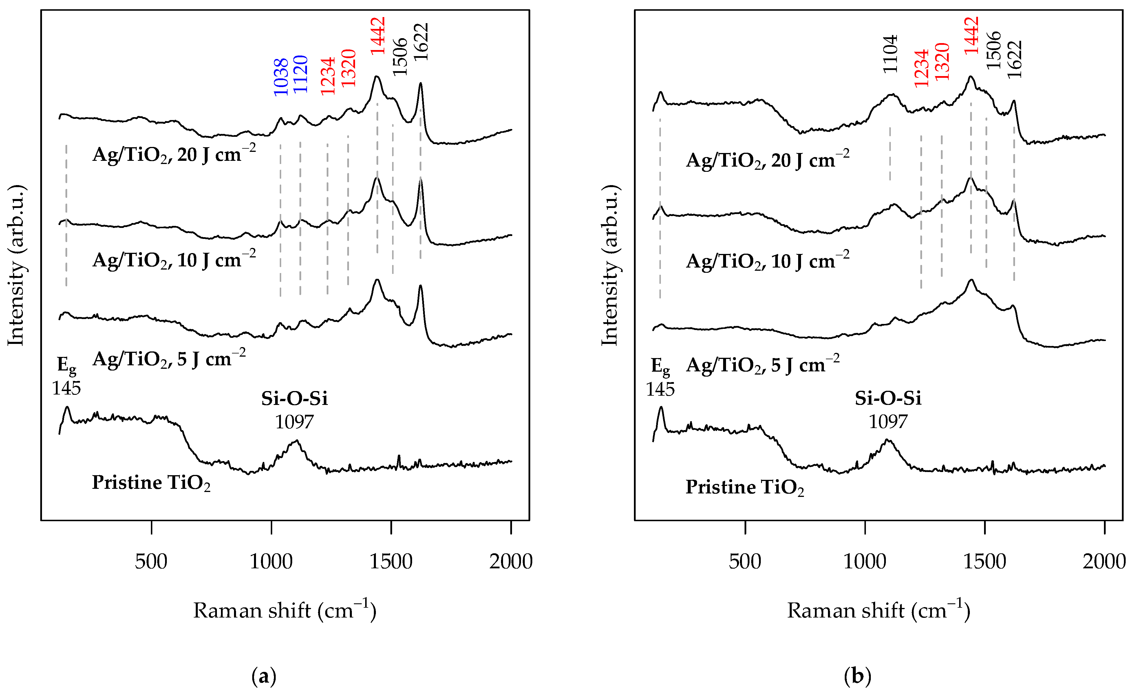
3.4. SERS Activity of the Ag-Functionalized TiO2 Grid Patterns

The appearance of surface-adsorbed species in the Raman spectra of the Ag-functionalized TiO2 samples suggested the possibility of utilizing surface-enhanced Raman scattering (SERS) amplification to detect MB adsorbates during the PCO activity experiments. To explore this potential, Raman spectra were recorded for both pristine TiO₂/ITO and Ag-functionalized TiO2 laser-patterned grids at two time points—after 60 min of dark-phase MB adsorption, and at the conclusion of the eighth MB PCO cycle. The results are presented in Figure 11a,b, respectively.
As seen in Figure 11a, the Raman spectra of the pristine TiO2 grids show no significant features other than the characteristic anatase TiO2 bands and the Si–O–Si stretching vibration from the glass substrate. In contrast, the Ag-functionalized TiO2 samples display pronounced differences. After dark-phase MB adsorption, the samples treated at 5, 10, and 20 J cm−2 exhibit intense Raman bands corresponding to MB vibrational modes. These include peaks at 1622 cm−1 and 1506 cm−1, associated with symmetric ν(C=C) stretching of the conjugated ring system; peaks at 1442 cm−1, 1320 cm−1, and 1234 cm−1, attributed to ν(C–N) stretching; and bands at 1120 cm−1 and 1038 cm−1, corresponding to out-of-plane and in-plane δ(C–H) bending vibrations [73,74,75].
Following eight full cycles of MB PCO activity testing, notable changes were observed in the Raman spectra of the Ag/TiO2 samples (Figure 11b). The SERS effect again enabled detection of surface species, but key MB vibrational bands—particularly the ν(C=C) band at 1622 cm−1 and the ν(C–N) modes in the 1400–1200 cm−1 range—were significantly suppressed. This suppression was especially pronounced for the sample functionalized at 20 J cm−2, consistent with spectral features of MB photodegradation products reported by Balu et al. [74].
Additionally, a broad Raman band appeared between 1060 and 1120 cm−1, centered around 1104 cm−1. This band can be attributed to C–O stretching vibrations of MB degradation intermediates, further supporting the hypothesis that SERS enables monitoring of MB decomposition pathways on the Ag/TiO2 surface under photocatalytic conditions [74].

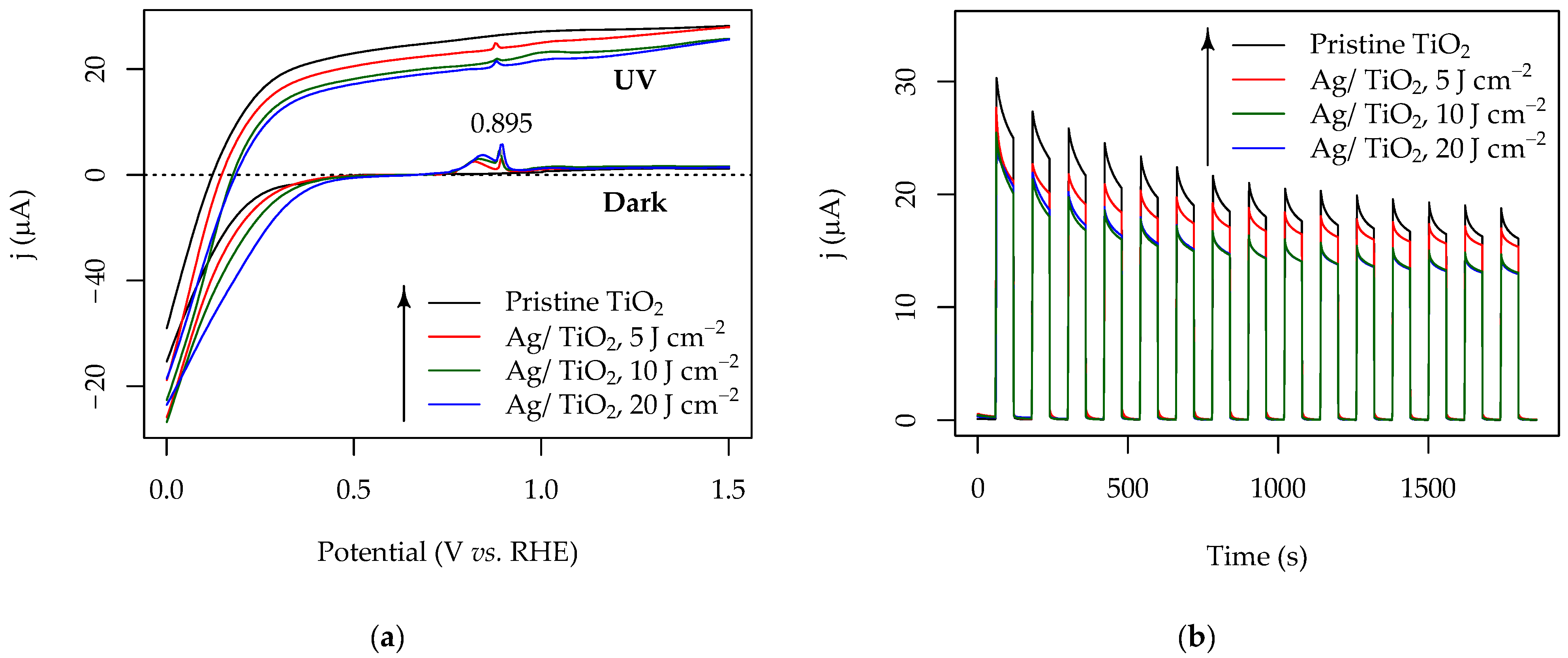
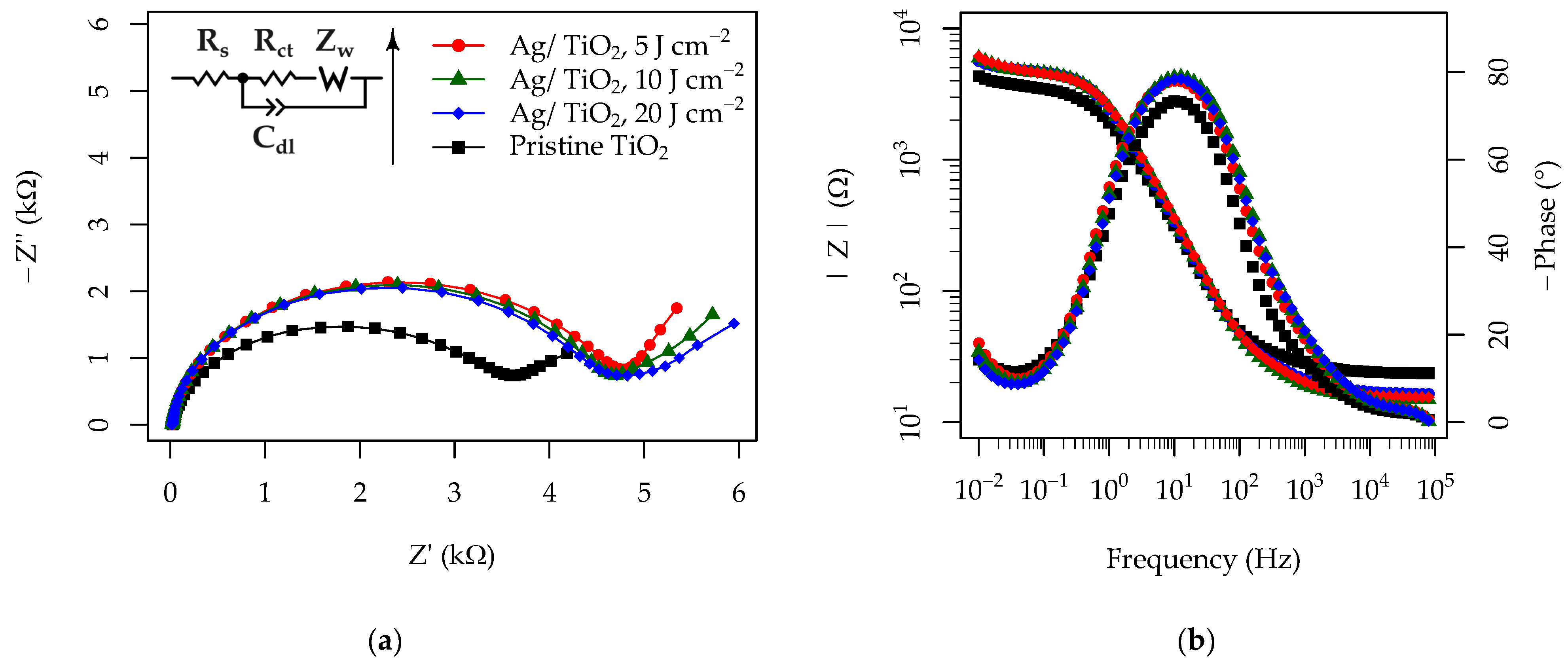
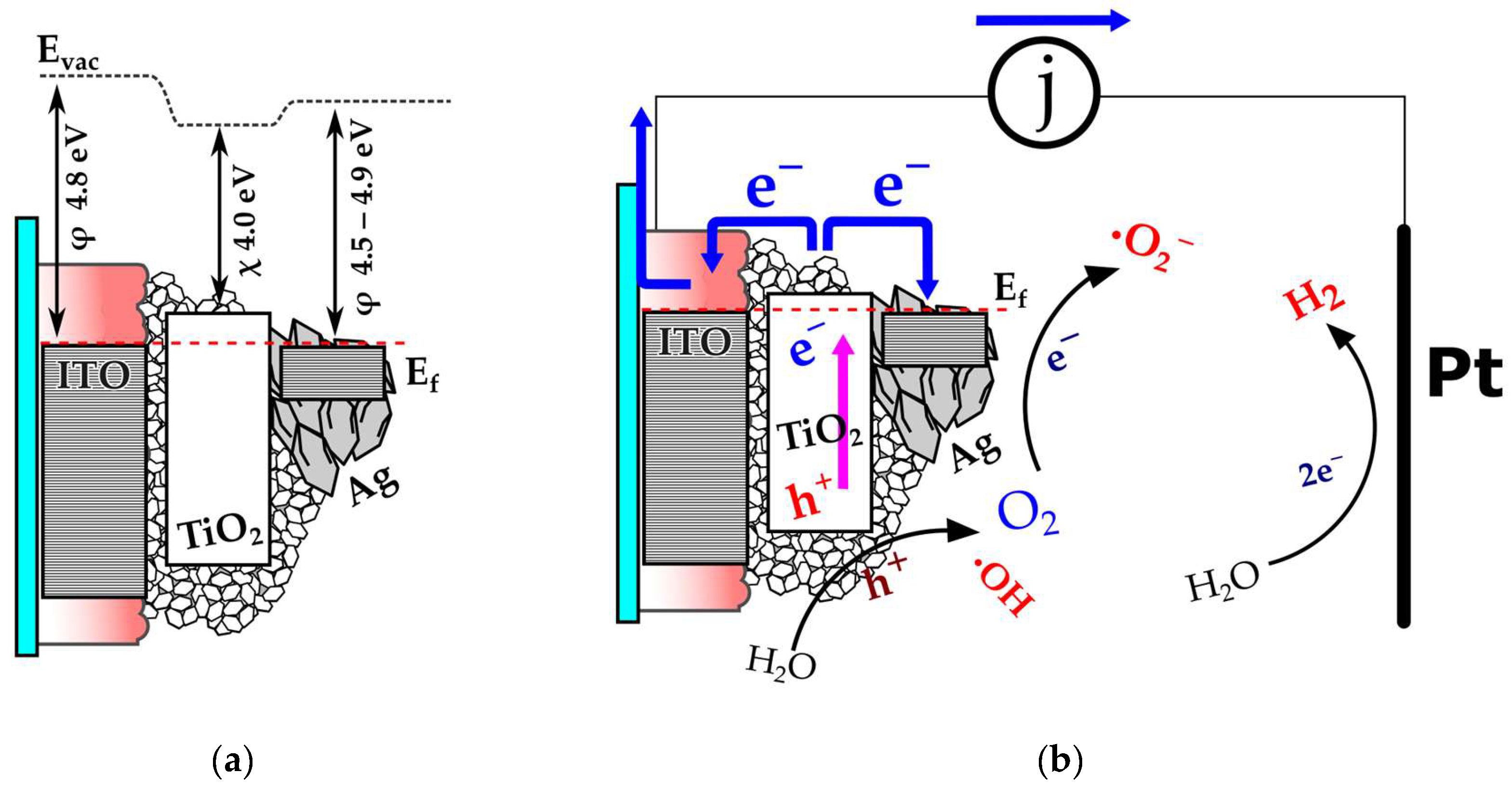
3.5. Photoelectrochemical Properties of the Pristine and Ag-Functionalized TiO2 Grid Patterns

Given the advantage of the TiO2 layer already being deposited on an ITO substrate, photoelectrochemical (PEC) measurements were performed to probe the behavior of both pristine and Ag-functionalized laser-patterned TiO2 layers. Figure 12a presents the linear sweep voltammetry (LSV) results for the pristine and Ag/TiO2 grids over a potential range of 0 to 1.5 V vs. RHE, under both dark and UV-illuminated conditions (with I U V = 6.9 mW cm−2).
Under dark conditions, minimal photocurrent was observed for all samples. However, an anodic peak was detected at approximately 0.895 V vs. RHE, with intensity increasing proportionally to the UV photodeposition dose ( D U V ). This peak can be attributed to the oxidation of metallic Ag0 to Ag2O, as reported in previous studies [76,77]. The presence of this peak in the absence of UV illumination also suggests that a significant portion of the Ag is deposited directly onto the ITO surface. Under UV illumination, the photocurrent behavior diverged from the photocatalytic activity trends observed in the MB PCO experiments. Interestingly, the pristine TiO2 sample exhibited the highest photocurrent density ( j ), with a positive j dependence on the applied potential, typical of TiO2-based photoanodes. In contrast, an inverse relationship between D U V and photocurrent was observed, with increasing photodeposition doses leading to lower j values. This trend was further confirmed by chronoamperometry measurements (Figure 12b), conducted at a constant potential of 1.23 V vs. RHE under pulsed UV illumination (15 cycles of 60 s light pulses over 30 min). All samples showed a gradual decline in photocurrent, stabilizing after ~15 min, while the general trend of lower photocurrent in Ag-functionalized samples remained consistent.
Electrochemical impedance spectroscopy (EIS) measurements at open circuit potential (OCP) are shown in Figure 13. The Bode plots (Figure 13b) show a single time-constant, while the Nyquist plots (Figure 13a) show larger semicircles for the Ag/TiO2 samples, indicating increased charge transfer resistance compared to the pristine sample. The electrochemical impedance spectroscopy (EIS) data were analyzed using the Randles equivalent circuit model (shown as an inset in Figure 13a). The extracted fitting parameters are summarized in Table 3, alongside the corresponding photocurrents ( j ) obtained from chronoamperometry measurements (Figure 12b). The table includes values for the series resistance ( R s ), charge-transfer resistance ( R c t ), constant phase element parameters ( C P E d l : capacitance and α ), and Warburg impedance ( Z W ).
The results confirm that the incorporation of Ag into the patterned TiO2/ITO surfaces leads to an increase in R c t and a corresponding decrease in photocurrent density. Although initially surprising, this result is consistent with previous reports on patterned TiO2 surfaces. He et al. [78], for instance, also observed reduced photocurrent following Ag photodeposition and attributed it to the formation of a TiO2/Ag Schottky junction, which can act as an electron sink. The Ag phase can scavenge photogenerated electrons and transfer them to dissolved oxygen, promoting the formation of reactive O2 radicals. This mechanism explains the enhanced PCO activity observed for Ag/TiO2 despite the lower photocurrent.
To confirm the presence of a TiO2/Ag Schottky junction, Mott–Schottky (M–S) analysis was performed, and the results are presented in Figure 14.
The measurements were conducted at four AC frequencies (500, 1000, 1500, and 2000 Hz). Flat-band potentials ( E f b ) were extracted by applying a linear fit to the step-like rise in inverse squared capacitance ( C 2 ) versus applied potential in the −0.25 to 1.0 V vs. RHE range.
The pristine TiO2 sample (Figure 14a) exhibited a single-step M–S plot, while all Ag-functionalized samples (Figure 14b–d) showed an additional step, indicative of a semiconductor–metal heterojunction. Similar dual-step features have been reported for noble metal-functionalized TiO2 photoanodes [79,80].
The first E f b step, attributed to the TiO2 phase, remained relatively stable across samples at −0.23 ± 0.01 V vs. RHE, shifting slightly to −0.25 ± 0.01 V for the 20 J cm−2 Ag/TiO2 sample. These values are significantly more negative than the literature-reported E f b of +0.163 V vs. RHE for polycrystalline anatase [81]. However, it is known that for patterned TiO2 photoanodes with exposed ITO regions, E f b tends to shift depending on TiO2 coverage, as demonstrated by Chen et al. [82].
A more notable difference was observed in the second E f b , associated with the Schottky junction. This potential was found to increase with photodeposition dose, measured as 0.69 ± 0.02 V, 0.73 ± 0.02 V, and 0.74 ± 0.01 V vs. RHE for the 5, 10, and 20 J cm−2 Ag/TiO2 samples, respectively. These values correlate with the initial MB PCO activity trends, suggesting that the Schottky barrier height is dependent on the photodeposition conditions and likely governs the charge separation efficiency in noble metal-functionalized TiO2 photocatalysts.
The conduction band (CB) edge of anatase TiO2 has been estimated at approximately χ ≈ 4.0 eV below the vacuum level (−0.5 V vs. NHE), both computationally and experimentally [83,84]. The higher work function of ITO (φ ≈ 4.8 eV) leads to the formation of a heterojunction at the TiO2/ITO interface [42]. The work function of silver (Ag) is facet-dependent, but for the (111) plane—which appears to dominate the photodeposited Ag phase based on XRD data (see Figure 8a)—it is estimated at φ ≈ 4.5 eV [85]. This value is known to be significantly influenced by surface-bound ions or oxidation, with variations of ±0.5 eV reported [86,87].
Based on these values, a band-energy diagram of the Ag/TiO2/ITO system can be constructed, as shown in Figure 15. In Figure 15a, the energy levels are aligned relative to the vacuum energy, using the electron affinity of TiO2 (representing the CB position) and the work functions of ITO and Ag. The resulting energy difference between the TiO2 CB and the system’s Fermi level falls within the range of 0.5–0.9 eV, which is consistent with the 0.94–0.95 V difference between the two flat-band potential ( E f b ) steps observed in the Mott–Schottky plots (see Figure 14).
Under UV illumination (Figure 15b), the TiO2/ITO heterojunction facilitates photogenerated electron transfer toward the ITO substrate under an applied positive bias [42]. However, the secondary Schottky junction formed between TiO2 and the photodeposited Ag phase results in electron accumulation on the Ag domains. These domains serve as electron sinks [78,88], promoting electron transfer to dissolved oxygen to generate superoxide radicals (•O₂). This mechanism contributes to the observed loss in photocurrent (Figure 12b) and supports the enhanced photocatalytic activity noted in the Ag-functionalized samples.

4. Conclusions

This work successfully demonstrates a cost-effective approach for fabricating patterned TiO2 surfaces using a colored salicylate-based TiO2 deposition sol, which can be processed via wet-chemical dip-coating and patterned using a low-power, off-the-shelf desktop laser engraver. Well-defined TiO2 mesh grids were formed with good spatial precision, sufficient to enable more complex pattern designs. Importantly, the laser processing did not hinder the crystallization of the sol–gel-derived layer into polycrystalline anatase TiO2.
Post-deposition functionalization of the TiO2 patterns via UV-induced photodeposition of silver (Ag) was also demonstrated. Due to the presence of the underlying ITO substrate, the photodeposited Ag species were preferentially localized at the TiO2/ITO interface, suggesting the formation of a TiO2/ITO heterojunction that influences deposition behavior. Photoelectrochemical characterization further confirmed the formation of Ag/TiO2 Schottky junctions in the functionalized samples.
All samples exhibited photocatalytic activity, as shown in methylene blue (MB) degradation experiments. A ~20% enhancement in activity was observed for the Ag-functionalized samples. However, due to the thin nature of the TiO2 layer, progressive photocatalyst deactivation was observed across eight consecutive MB oxidation cycles, with activity losses reaching up to 50%. Notably, the Ag-functionalized samples also exhibited surface-enhanced Raman scattering (SERS) activity, enabling the detection of the Raman signature for surface adsorbed MB molecules.
While preliminary, this study highlights multiple directions for future development. First, optimization of laser parameters (e.g., power and feed rate) could achieve direct crystallization without the need for post-annealing. Second, the patterned TiO2/ITO architecture presents a promising platform for fabricating more complex additively manufactured devices, such as sensors or energy conversion systems. Third, the observed SERS activity offers opportunities to further study molecular interactions at metal-functionalized TiO2 interfaces, with potential applications in surface sensing and photocatalysis monitoring.

Funding

The author acknowledges that the full financial support for this study was provided by the Bulgarian National Science Fund (BNSF), under project KП-06-H59/11 “Photocatalytic activity of thin films with selectively photodeposited cocatalysts”.

Institutional Review Board Statement

Not applicable.

Informed Consent Statement

Not applicable.

Data Availability Statement

The original contributions presented in the study are included in the article. Further inquiries can be directed to the corresponding author.

Acknowledgments

The provision of access to, and use of research equipment of distributed research infrastructure INFRAMAT (part of Bulgarian National roadmap for research infrastructures) supported by Bulgarian Ministry of Education and Science for the purposes of this study is greatly acknowledged.

Conflicts of Interest

The author declares no conflicts of interest. The funder had no role in the design of the study; in the collection, analyses, or interpretation of data; in the writing of the manuscript; or in the decision to publish the results.

References

  1. Scheider, J.; Matsuoka, M.; Takeuchi, M.; Zhang, J.; Horiuchi, Y.; Anpo, M.; Bahnemann, D.W. Understanding TiO2 Photocatalysis: Mechanisms and Materials. Chem. Rev. 2014, 114, 9919–9986. [Google Scholar] [CrossRef] [PubMed]
  2. Fujishima, A.; Zhang, X.; Tryk, D.A. TiO2 photocatalysis and related surface phenomena. Surf. Sci. Rep. 2008, 63, 515–582. [Google Scholar] [CrossRef]
  3. Morshedy, A.S.; El-Fawal, E.M.; Zaki, T.; El-Zahhar, A.A.; Alghamdi, M.M.; El Naggar, A.M.A. A review on heterogeneous photocatalytic materials: Mechanism, perspectives, and environmental and energy sustainability applications. Inorg. Chem. Commun. 2024, 163, 112307. [Google Scholar] [CrossRef]
  4. Yang, X.; Zhao, R.; Zhan, H.; Zhao, H.; Duan, Y.; Shen, Z. Modified Titanium dioxide-based photocatalysts for water treatment: Mini review. Environ. Funct. Mater. 2024, 3, 1–12. [Google Scholar] [CrossRef]
  5. Armaković, S.J.; Savanović, M.M.; Armaković, S. Titanium Dioxide as the Most Used Photocatalyst for Water Purification: An Overview. Catalysts 2023, 13, 26. [Google Scholar] [CrossRef]
  6. Kumar, L.; Ragunathan, V.; Chugh, M.; Bharadvaja, N. Nanomaterials for remediation of contaminants: A review. Environ. Chem. Lett. 2021, 19, 3139–3163. [Google Scholar] [CrossRef]
  7. Ismael, M. A review and recent advances in solar-to-hydrogen energy conversion based on photocatalytic water splitting over doped-TiO2 nanoparticles. Sol. Energy 2021, 19, 3139–3163. [Google Scholar] [CrossRef]
  8. Xu, Y.; Zangari, G. TiO2 Nanotubes Architectures for Solar Energy Conversion. Coatings 2021, 11, 931. [Google Scholar] [CrossRef]
  9. Zhou, C.; Xi, Z.; Stacchiola, D.J.; Liu, M. Application of ultrathin TiO2 layers in solar energy conversion devices. Energy Sci. Eng. 2022, 10, 1614–1629. [Google Scholar] [CrossRef]
  10. Kumar, A.; Choudhary, P.; Kumar, A.; Camargo, P.H.C.; Krishnan, V. Recent Advances in Plasmonic Photocatalysis Based on TiO2 and Noble Metal Nanoparticles for Energy Conversion, Environmental Remediation, and Organic Synthesis. Small 2021, 18, 2101638. [Google Scholar] [CrossRef]
  11. Ahmad, M.S.; Pandey, A.K.; Rahim, N.A. Advancements in the development of TiO2 photoanodes and its fabrication methods for dye sensitized solar cell (DSSC) applications. A review. Renew. Sustain. Energy Rev. 2017, 77, 89–108. [Google Scholar] [CrossRef]
  12. Kaur, G.; Negi, P.; Konwar, R.J.; Kumar, H.; Devi, N.; Kaur, G.; Himani; Kaur, M.; Sharma, R.; Sati, P.C.; et al. Tailored TiO2 nanostructures for designing of highly efficient dye sensitized solar cells: A review. Nano-Struct. Nano-Objects 2023, 36, 101056. [Google Scholar] [CrossRef]
  13. Yan, Y.; Zhang, Y.; Zhao, Y.; Ding, F.; Lei, Y.; Wang, Y.; Zhou, J.; Kang, W. Review on TiO2 nanostructured photoanode and novel dyes for dye-sensitized solar cells application. J. Mater. Sci. 2025, 60, 4975–5005. [Google Scholar] [CrossRef]
  14. Ge, S.; Sang, D.; Zou, L.; Yao, Y.; Zhou, C.; Fu, H.; Xi, H.; Fan, L.; Wang, C. A Review on the Progress of Optoelectronic Devices Based on TiO2 Thin Films and Nanomaterials. Nanomaterials 2023, 13, 1141–2023. [Google Scholar] [CrossRef]
  15. Hazra, S.; Singh, S.V.; Dahiya, S.; Aich, P.K.; Pal, B.N. Solution-Processed Ag-TiO2 Nanostructure-Based Schottky Junction Thin Films for Narrowband Hot-Electron Photodetectors. ACS Appl. Nano Mater. 2023, 6, 15119–15127. [Google Scholar] [CrossRef]
  16. Wang, Y.-H.; Rahman, K.H.; Wu, C.-C.; Chen, K.-C. A Review on the Pathways of the Improved Structural Characteristics and Photocatalytic Performance of Titanium Dioxide (TiO2) Thin Films Fabricated by the Magnetron-Sputtering Technique. Catalysts 2020, 10, 598. [Google Scholar] [CrossRef]
  17. Vahl, A.; Veziroglu, S.; Henkel, B.; Strunskus, T.; Polonskyi, O.; Aktas, O.C.; Faupel, F. Pathways to Tailor Photocatalytic Performance of TiO2 Thin Films Deposited by Reactive Magnetron Sputtering. Materials 2019, 12, 2840. [Google Scholar] [CrossRef]
  18. Simionescu, O.-G.; Romanițan, C.; Tutunaru, O.; Ion, V.; Buiu, O.; Avram, A. RF Magnetron Sputtering Deposition of TiO2 Thin Films in a Small Continuous Oxygen Flow Rate. Coatings 2019, 9, 442. [Google Scholar] [CrossRef]
  19. Dong, X.; Mamat, M.; Baikeli, Y. Effect of annealing temperature on the structural, optical, morphological, and photocatalytic properties of TiO2 thin films prepared by sol-gel spin-coating and electron beam physical vapor deposition. J. Phys. D Appl. Phys. 2024, 57, 385106. [Google Scholar] [CrossRef]
  20. Azpiroz, R.; Borraz, M.; González, A.; Mansilla, C.; Iglesias, M.; Pérez-Torrente, J.J. Photocatalytic Activity in the In-Flow Degradation of NO on Porous TiO2–Coated Glasses from Hybrid Inorganic–Organic Thin Films Prepared by a Combined ALD/MLD Deposition Strategy. Coatings 2022, 12, 488. [Google Scholar] [CrossRef]
  21. Zimbone, M.; Cantarella, M.; Sfuncia, G.; Nicotra, G.; Privitera, V.; Napolitani, E.; Impellizzeri, G. Low-temperature atomic layer deposition of TiO2 activated by laser annealing: Applications in photocatalysis. Appl. Surf. Sci. 2022, 596, 153641. [Google Scholar] [CrossRef]
  22. Noorasid, N.S.; Arith, F.; Aliyaselvam, O.V.; Salehuddin, F.; Mustafa, A.N.; Chelvanathan, P.; Azam, M.A.; Amin, N. Low-temperature sol-gel synthesized TiO2 with different titanium tetraisopropoxide (TTIP) molarity for flexible emerging solar cell. J. Sol-Gel Sci. Technol. 2024, 109, 826–834. [Google Scholar] [CrossRef]
  23. Rola, K.P.; Duda, L.; Gorantla, S.; Czyż, K.; Guzik, M.; Cybińska, J. Focused Electron Beam Micro- and Nanopatterning of Thin Films Derived from Sol–Gels Based on TiO2 Precursors for Planar Photonics. ACS Appl. Nano Mater. 2024, 7, 8692–8702. [Google Scholar] [CrossRef]
  24. Ivanova, T.; Harizanova, A.; Koutzarova, T.; Vertruyen, B. Preparation and Investigation of Sol–Gel TiO2-NiO Films: Structural, Optical and Electrochromic Properties. Crystals 2024, 14, 192. [Google Scholar] [CrossRef]
  25. Efeoglu, H.; Güllülü, S.; Karacali, T. Resistive switching of reactive sputtered TiO2 based memristor in crossbar geometry. Appl. Surf. Sci. 2015, 350, 10–13. [Google Scholar] [CrossRef]
  26. Ratova, M.; Sawtell, D.; Kelly, P.J. Micro-Patterning of Magnetron Sputtered Titanium Dioxide Coatings and Their Efficiency for Photocatalytic Applications. Coatings 2020, 10, 68. [Google Scholar] [CrossRef]
  27. Abshari, F.; Veziroglu, S.; Adejube, B.; Vahl, A.; Gerken, M. Photocatalytic Edge Growth of Conductive Gold Lines on Microstructured TiO2–ITO Substrates. Langmuir 2024, 40, 19051–19059. [Google Scholar] [CrossRef]
  28. Wu, C.-T.; Soliman, A.I.A.; Tu, Y.; Utsunomiya, T.; Ichii, T.; Sugimura, H. Fabrication of TiO2 Micropatterns on Flexible Substrates by Vacuum-Ultraviolet Photochemical Treatments. Adv. Mater. Interfaces 2020, 7, 1901634. [Google Scholar] [CrossRef]
  29. Shavdina, O.; Berthod, L.; Kämpfe, T.; Reynaud, S.; Veillas, C.; Verrier, M.; Vocanson, F.; Fugier, P.; Jourlin, Y.; Dellea, O. Large Area Fabrication of Periodic TiO2 Nanopillars Using Microsphere Photolithography on a Photopatternable Sol–Gel Film. Langmuir 2015, 31, 7877–7884. [Google Scholar] [CrossRef]
  30. Crespo-Monteiro, N.; Hamandi, M.; Usuga Higuita, M.A.; Guillard, C.; Dappozze, F.; Jamon, D.; Vocanson, F.; Jourlin, Y. Influence of the Micro-Nanostructuring of Titanium Dioxide Films on the Photocatalytic Degradation of Formic Acid under UV Illumination. Nanomaterials 2022, 12, 1008. [Google Scholar] [CrossRef]
  31. Starbova, K.; Yordanova, V.; Nihtianova, D.; Hintz, W.; Tomas, J.; Starbov, J. Excimer laser processing as a tool for photocatalytic design of sol–gel TiO2 thin films. Appl. Surf. Sci. 2008, 254, 4044–4051. [Google Scholar] [CrossRef]
  32. Bougdid, Y.; Chenard, F.; Sugrim, J.; Kumar, R.; Kar, A. CO2 laser-assisted sintering of TiO2 nanoparticles for transparent films. J. Laser Appl. 2023, 35, 012012. [Google Scholar] [CrossRef]
  33. Bougdid, Y.; Kulkarni, G.; Chenard, F.; Sugrim, C.J.; Kumar, R.; Kar, A. Optical properties of transparent TiO2 films by sintering anatase nanoparticles with a CO2 laser. Opt. Mater. 2024, 156, 115969. [Google Scholar] [CrossRef]
  34. Noel, L.; Khitous, A.; Molinaro, C.; Zan, H.-W.; Berling, D.; Grasset, F.; Soppera, O. Laser Direct Writing of Crystallized TiO2 by Photothermal Effect Induced by Gold Nanoparticles. Adv. Mater. Technol. 2024, 9, 2300407. [Google Scholar] [CrossRef]
  35. Gerlein, L.F.; Benavides-Guerrero, J.A.; Cloutier, S.G. Laser-Assisted, Large-Area Selective Crystallization and Patterning of Titanium Dioxide Polymorphs. Adv. Eng. Mater. 2020, 22, 1901014. [Google Scholar] [CrossRef]
  36. Stefanov, B.I. Optically Transparent TiO2 and ZnO Photocatalytic Thin Films via Salicylate-Based Sol Formulations. Coatings 2023, 13, 1568. [Google Scholar] [CrossRef]
  37. Huang, L.; Liu, X.; Wu, H.; Wang, X.; Wu, H.; Li, R.; Shi, L.; Li, C. Surface state modulation for size-controllable photodeposition of noble metal nanoparticles on semiconductors. J. Mater. Chem. A 2020, 8, 21094–21102. [Google Scholar] [CrossRef]
  38. Butburee, T.; Kotchasarn, P.; Hirunsit, P.; Sun, Z.; Tang, Q.; Khemthong, P.; Sangkhun, W.; Thongsuwan, W.; Kumnorkaew, P.; Wang, H.; et al. New understanding of crystal control and facet selectivity of titanium dioxide ruling photocatalytic performance. J. Mater. Chem. A 2019, 7, 8156–8166. [Google Scholar] [CrossRef]
  39. Bai, S.; Jiang, J.; Zhang, Q.; Xiong, Y. Steering charge kinetics in photocatalysis: Intersection of materials syntheses, characterization techniques and theoretical simulations. Chem. Soc. Rev. 2015, 44, 2893–2939. [Google Scholar] [CrossRef]
  40. El-Zohry, A.M.; Kloo, L.; He, L. Understanding Charge Dynamics in TiO2 Using Ultrafast Mid-infrared Spectroscopy: Trapping versus Recombination. J. Phys. Chem. C 2024, 128, 4192–4199. [Google Scholar] [CrossRef]
  41. Okazaki, M.; Suganami, Y.; Hirayama, N.; Nakata, H.; Oshikiri, T.; Yokoi, Y.; Misawa, H.; Maeda, K. Site-Selective Deposition of a Cobalt Cocatalyst onto a Plasmonic Au/TiO2 Photoanode for Improved Water Oxidation. ACS Appl. Energy Mater. 2020, 3, 5142–5146. [Google Scholar] [CrossRef]
  42. Dai, W.; Wang, X.; Liu, P.; Xu, Y.; Li, G.; Fu, X. Effects of Electron Transfer between TiO2 Films and Conducting Substrates on the Photocatalytic Oxidation of Organic Pollutants. J. Phys. Chem. B 2006, 110, 13470–13476. [Google Scholar] [CrossRef] [PubMed]
  43. Abshari, F.; Paulsen, M.; Veziroglu, S.; Vahl, A.; Gerken, M. ITO-TiO2 Heterojunctions on Glass Substrates for Photocatalytic Gold Growth Along Pattern Edges. Catalysts 2024, 14, 940. [Google Scholar] [CrossRef]
  44. Stefanov, B.I.; Kolev, H.G. MnOx and Pd Surface Functionalization of TiO2 Thin Films via Photodeposition UV Dose Control. Photochem 2024, 4, 474–487. [Google Scholar] [CrossRef]
  45. Stefanov, B. Photocatalytic reactor for in situ determination of supported catalysts activity in liquid-phase based on 3D-printed components and Arduino. In Proceedings of the 2020 XXIX International Scientific Conference Electronics (ET), Sozopol, Bulgaria, 16–18 September 2020. [Google Scholar] [CrossRef]
  46. Swanepoel, R. Determination of the thickness and optical constants of amorphous silicon. J. Phys. E Sci. Instrum. 1983, 16, 1214. [Google Scholar] [CrossRef]
  47. Kubinyi, M.; Benkö, N.; Grofcsik, A.; Jeremy Jones, W. Determination of the thickness and optical constants of thin films from transmission spectra. Thin Solid Films 1996, 286, 164–169. [Google Scholar] [CrossRef]
  48. Kerscher, M.; Braun, L.M.; Jander, J.H.; Rausch, M.H.; Koller, T.M.; Wasserscheid, P.; Fröba, A.P. Viscosity, Interfacial Tension, and Density of 2-Propanol and Acetone up to 423 K by Surface Light Scattering and Conventional Methods. Int. J. Thermophys. 2024, 45, 8. [Google Scholar] [CrossRef]
  49. Amrhein, S.; Bauer, K.C.; Galm, L.; Hubbuch, J. Non-invasive high throughput approach for protein hydrophobicity determination based on surface tension. Biotechnol. Bioeng. 2015, 112, 2485–2494. [Google Scholar] [CrossRef]
  50. de Gennes, P.G.; Brochard-Wyart, F.; Quéré, D. Hysteresis and Elasticity of Triple Lines. In Capillarity and Wetting Phenomena; Springer: New York, NY, USA, 2004. [Google Scholar] [CrossRef]
  51. Zhang, Z.; Peng, F.; Kornev, K.G. The Thickness and Structure of Dip-Coated Polymer Films in the Liquid and Solid States. Micromachines 2022, 13, 982. [Google Scholar] [CrossRef]
  52. Colusso, E.; Basso, M.; Carraro, C.; Cesaroni, C.; Di Russo, E.; Guglielmi, M.; Napolitani, E.; Martucci, A. Pulsed laser crystallization of sol-gel derived cerium oxide thin films. J. Sol-Gel Sci. Technol. 2025, 114, 75–86. [Google Scholar] [CrossRef]
  53. Matsubayashi, Y.; Nomoto, J.; Yamaguchi, I.; Tsuchiya, T. Control of the oxygen deficiency and work function of SrFeO3−δ thin films by excimer laser- assisted metal organic decomposition. CrystEngComm 2020, 22, 4685. [Google Scholar] [CrossRef]
  54. Txintxurreta, J.; G-Berasategui, E.; Ortiz, R.; Hernández, O.; Mendizábal, L.; Barriga, J. Indium Tin Oxide Thin Film Deposition by Magnetron Sputtering at Room Temperature for the Manufacturing of Efficient Transparent Heaters. Coatings 2021, 11, 92. [Google Scholar] [CrossRef]
  55. Veziroglu, S. Fabrication of Ultra-Fine Ag NPs on TiO2 Thin Films by Alcohol-Assisted Photodeposition Process for Photocatalysis-Related Applications. Materials 2024, 17, 1354. [Google Scholar] [CrossRef] [PubMed]
  56. Tian, F.; Zhang, Y.; Zhang, J.; Pan, C. Raman Spectroscopy: A New Approach to Measure the Percentage of Anatase TiO2 Exposed (001) Facets. J. Phys. Chem. C 2012, 116, 7515–7519. [Google Scholar] [CrossRef]
  57. Liu, H.; Kaya, H.; Lin, Y.-T.; Ogrinc, A.; Kim, S.H. Vibrational spectroscopy analysis of silica and silicate glass networks. J. Am. Ceram. Soc. 2022, 105, 2355–2384. [Google Scholar] [CrossRef]
  58. Shirpay, A.; Tavakoli, M. The behavior of the active modes of the anatase phase of TiO2 at high temperatures by Raman scattering spectroscopy. Ind. J. Phys. 2022, 96, 1673–1681. [Google Scholar] [CrossRef]
  59. Melvin, A.A.; Illath, K.; Das, T.; Raja, T.; Bhattacharyya, S.; Gopinath, C.S. M–Au/TiO2 (M = Ag, Pd, and Pt) nanophotocatalyst for overall solar water splitting: Role of interfaces. Nanoscale 2015, 7, 13477–13488. [Google Scholar] [CrossRef]
  60. Shan, W.; Liu, R.; Zhao, H.; He, Z.; Lai, Y.; Li, S.; He, G.; Liu, J. In Situ Surface-Enhanced Raman Spectroscopic Evidence on the Origin of Selectivity in CO2 Electrocatalytic Reduction. ACS Nano 2020, 14, 11363–11372. [Google Scholar] [CrossRef]
  61. Joshi, N.; Jain, N.; Pathak, A.; Singh, J.; Prasad, R.; Upadhyaya, C. Biosynthesis of silver nanoparticles using Carissa carandas berries and its potential antibacterial activities. J. Sol-Gel. Sci. Technol. 2018, 86, 682–689. [Google Scholar] [CrossRef]
  62. Pylnev, M.; Wong, M.-S. Comparative study of photocatalytic deactivation of pure and black titania thin films. J. Photochem. Photobiol. A Chem. 2019, 378, 125–130. [Google Scholar] [CrossRef]
  63. Tschirch, J.; Bahnemann, D.; Wark, M.; Rathouský, J. A comparative study into the photocatalytic properties of thin mesoporous layers of TiO2 with controlled mesoporosity. J. Photochem. Photobiol. A Chem. 2008, 194, 181–188. [Google Scholar] [CrossRef]
  64. Puga, F.; Navío, J.; Hidalgo, M. A critical view about use of scavengers for reactive species in heterogeneous photocatalysis. Appl. Catal. A Gen. 2024, 685, 119879. [Google Scholar] [CrossRef]
  65. Arunadevi, R.; Kavitha, B.; Rajarajan, M.; Suganthi, A. Synthesis of Ce/Mo-V4O9 nanoparticles with superior visible light photocatalytic activity for Rhodamine-B degradation. J. Environ. Chem. Eng. 2018, 6, 3349–3357. [Google Scholar] [CrossRef]
  66. Mills, A.; Wang, J. Photobleaching of methylene blue sensitized by TiO2: An ambiguous system? J. Photochem. Photobiol. A Chem. 1999, 127, 123–124. [Google Scholar] [CrossRef]
  67. Guo, M.; Ng, A.M.C.; Liu, F.; Djurišić, A.B.; Chan, W.K. Photocatalytic activity of metal oxides—The role of holes and OH radicals. Appl. Catal. B Environ. 2011, 107, 150–157. [Google Scholar] [CrossRef]
  68. Ishibashi, K.-I.; Fujishima, A.; Watanabe, T.; Hashimoto, K. Quantum yields of active oxidative species formed on TiO2 photocatalyst. J. Photochem. Photobiol. A 2000, 134, 139–142. [Google Scholar] [CrossRef]
  69. Liu, J.; Liu, H.; Zuo, X.; Wen, F.; Jiang, H.; Cao, H.; Pei, Y. Micro-patterned TiO2 films for photocatalysis. Matter. Lett. 2019, 254, 448–451. [Google Scholar] [CrossRef]
  70. Sidaraviciute, R.; Kavaliunas, V.; Puodziukynas, L.; Guobiene, A.; Martuzevicius, D.; Andrulevicius, M. Enhancement of photocatalytic pollutant decomposition efficiency of surface mounted TiO2 via lithographic surface patterning. Environ. Technol. Innov. 2020, 19, 100983. [Google Scholar] [CrossRef]
  71. Ponkratova, E.; Kuzmichev, A.; Rud, D.; Khubezhov, S.; Dolgintsev, D.; Ageev, E.; Veiko, V.; Sinev, D.; Zuev, D. Nanosecond Laser-Assisted Fabrication of Photocatalytically Active TiO2 Nanocoatings: Implication in Organic Dyes Degradation. ACS Appl. Nano Mater. 2024, 7, 19268–19278. [Google Scholar] [CrossRef]
  72. Bernhardt, A.; Lorentz, P.; Fischer, K.; Schmidt, M.; Kühnert, M.; Lotnyk, A.; Griebel, J.; Schönherr, N.; Zimmer, K.; Schulze, A. Laser-Crystallization of TiO2 Nanotubes for Photocatalysis: Influence of Laser Power and Laser Scanning Speed. Laser Photonics Rev. 2024, 18, 2300778. [Google Scholar] [CrossRef]
  73. Ruan, C.; Wang, W.; Gu, B. Single-molecule detection of thionine on aggregated gold nanoparticles by surface enhanced Raman scattering. J. Raman Spectrosc. 2007, 38, 568–573. [Google Scholar] [CrossRef]
  74. Balu, P.; Asharani, I.V.; Thirumalai, D. Catalytic degradation of hazardous textile dyes by iron oxide nanoparticles prepared from Raphanus sativus leaves’ extract: A greener approach. J. Mater. Sci. Mater. Electron. 2020, 31, 10669–10676. [Google Scholar] [CrossRef]
  75. Xiao, G.-N.; Man, S.-Q. Surface-enhanced Raman scattering of methylene blue adsorbed on cap-shaped silver nanoparticles. Chem. Phys. Lett. 2007, 447, 305–309. [Google Scholar] [CrossRef]
  76. Zheng, J.; Yu, H.; Li, X.; Zhang, S. Enhanced photocatalytic activity of TiO2 nano-structured thin film with a silver hierarchical configuration. Appl. Surf. Sci. 2008, 254, 1630–1635. [Google Scholar] [CrossRef]
  77. Katsiaounis, S.; Panidi, J.; Koutselas, I.; Topoglidis, E. Fully Reversible Electrically Induced Photochromic-Like Behaviour of Ag:TiO2 Thin Films. Coatings 2020, 10, 130. [Google Scholar] [CrossRef]
  78. He, C.; Xiong, Y.; Chen, J.; Zha, C.; Zhu, X. Photoelectrochemical performance of Ag–TiO2/ITO film and photoelectrocatalytic activity towards the oxidation of organic pollutants. J. Photochem. Photobiol. A Chem. 2003, 157, 71–79. [Google Scholar] [CrossRef]
  79. Syrek, K.; Czopor, J.; Topa-Skwarczyńska, M.; Pilch, M.; Kamiński, K.; Ortyl, J.; Sulka, G. Photoelectrochemical Properties of BODIPY-Sensitized Anodic TiO2 Layers Decorated with AuNPs for Enhanced Solar Performance. J. Phys. Chem. C 2023, 127, 9471–9480. [Google Scholar] [CrossRef]
  80. Wierbicka, E.; Schultz, T.; Syrek, K.; Sulka, G.; Koch, N.; Pinna, N. Ultra-stable self-standing Au nanowires/TiO2 nanoporous membrane system for high-performance photoelectrochemical water splitting cells. Mater. Horiz. 2022, 9, 2797–2808. [Google Scholar] [CrossRef]
  81. Kavan, L. Electrochemistry and band structure of semiconductors (TiO2, SnO2, ZnO): Avoiding pitfalls and textbook errors. J. Solid State Chem. 2024, 28, 829–845. [Google Scholar] [CrossRef]
  82. Chen, D.; Gao, Y.; Wang, G.; Zhang, H.; Lu, W.; Li, J. Surface Tailoring for Controlled Photoelectrochemical Properties: Effect of Patterned TiO2 Microarrays. J. Phys. Chem. C 2007, 111, 13163–13169. [Google Scholar] [CrossRef]
  83. Di Valentin, C.; Selloni, A. Bulk and Surface Polarons in Photoexcited Anatase TiO2. J. Phys. Chem. Lett. 2011, 2, 2223–2228. [Google Scholar] [CrossRef]
  84. Grätzel, M. Photoelectrochemical cells. Nature 2001, 414, 338–344. [Google Scholar] [CrossRef] [PubMed]
  85. Chelvayohan, M.; Mee, C. Work function measurements on (110), (100) and (111) surfaces of silver. J. Phys. C Solid State Phys. 1982, 15, 2305. [Google Scholar] [CrossRef]
  86. Seong, M.; Kim, H.; Lee, S.; Kim, D.; Oh, S. Engineering the work function of solution-processed electrodes of silver nanocrystal thin film through surface chemistry modification. APL Mater. 2018, 6, 121105. [Google Scholar] [CrossRef]
  87. Li, W.-X.; Stampfl, C.; Scheffler, M. Subsurface oxygen and surface oxide formation at Ag(111): A density-functional theory investigation. Phys. Rev. B 2003, 67, 045408. [Google Scholar] [CrossRef]
  88. Zhao, W.; Wen, L.; Parkin, I.; Zhao, X.; Liu, B. Fermi-level shift, electron separation, and plasmon resonance change in Ag nanoparticle-decorated TiO2 under UV light illumination. Phys. Chem. Chem. Phys. 2023, 25, 20134–20144. [Google Scholar] [CrossRef]
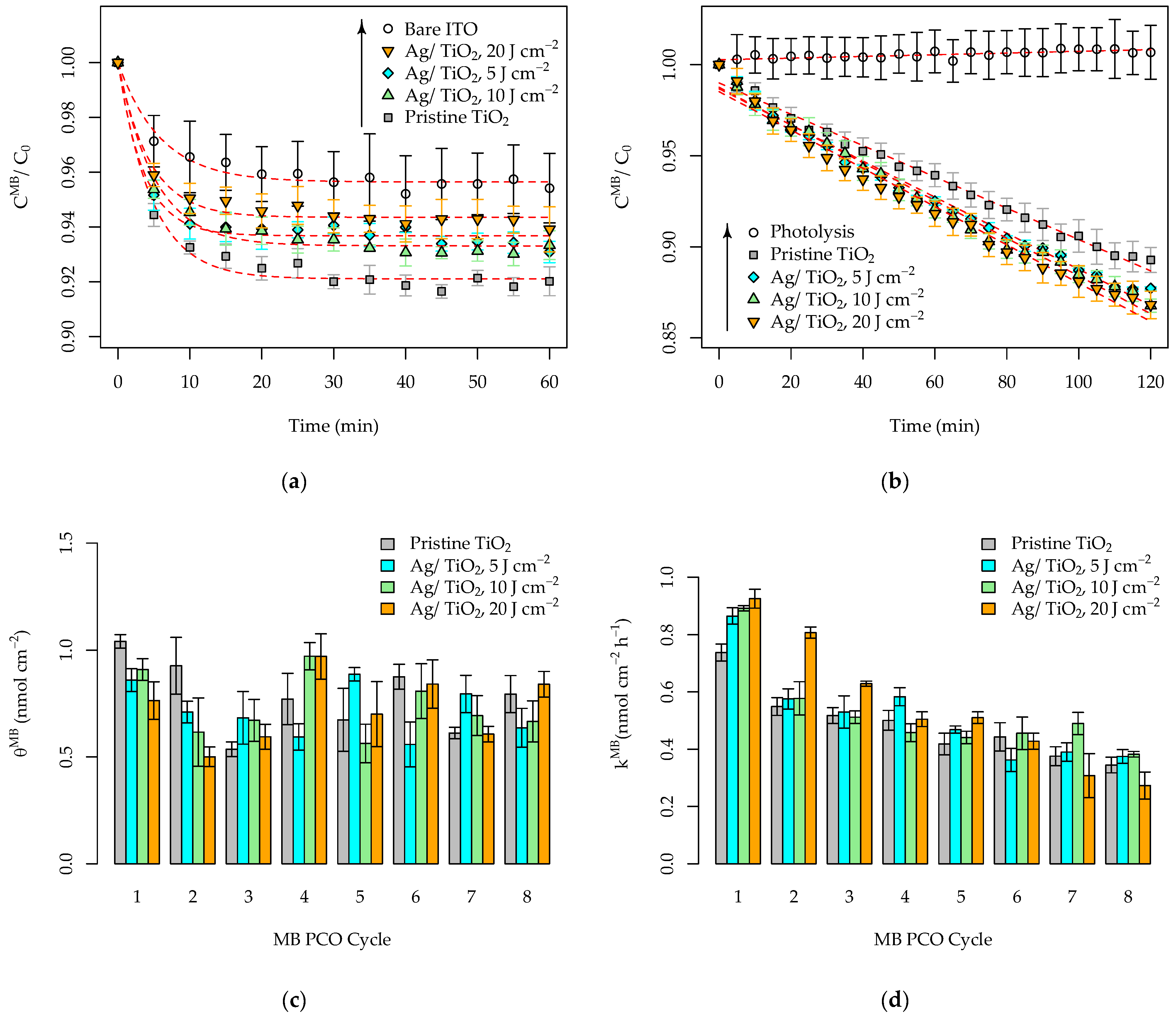
Figure 1. Schematic illustration of the fabrication process for laser-patterned, Ag-functionalized TiO2/ITO grids. Insets show photographic images of the substrate after each step.
Coatings 15 00709 g001
Figure 2. Screening of methylene blue (MB) photocatalytic oxidation (PCO) activity: (a) cross-sectional schematic of a single cell in the three-cell automated MB PCO setup; (b) example of an MB concentration profile ( C M B ) obtained for a pristine TiO2/ITO patterned grid, showing the 60 min dark phase and the subsequent 120 min UV illumination phase. The applied fits for determining MB saturation coverage ( θ M B ) and photocatalytic oxidation rate ( k M B ) are shown, along with comparative data from a blank experiment using an uncoated ITO substrate.
Coatings 15 00709 g002
Figure 3. UV–Vis transmittance spectrum of the dip-coated salicylate TiO2 sol layer, with the positions of the interference fringes maxima noted, overlaid with the emission spectrum of the 445 nm laser diode used for patterning.
Coatings 15 00709 g003
Figure 4. ATR-FTIR spectra of the TiO2 sol at different stages sample preparation (refer to Figure 1 for step descriptions). Peaks marked with ● correspond to the Ti[SA]3 complex, while those marked with □ are attributed to the IPA solvent.
Coatings 15 00709 g004
Figure 5. Optical micrographs (100× magnification) showing microstructural evolution of the laser-patterned TiO2 sol layer: (a) as-deposited dry sol layer; (b) laser-patterned sol layer; (c) laser-patterned layer after acetone rinse; (d) final TiO2 grid pattern after annealing.
Coatings 15 00709 g005
Figure 6. SEM–EDS analysis of the pristine TiO2 and Ag-functionalized laser-patterned coatings: (a) low-magnification image of the pristine TiO2 grid; (b) higher-magnification image of a TiO2 trace; (c) EDS maps showing Ti and In distribution at the grid edge; (d) low-magnification image of Ag/TiO2 grid patterned at 20 J cm−2; (e) higher-magnification image of the TiO2 trace; (f) EDS maps showing Ti and Ag distribution.
Coatings 15 00709 g006
Figure 7. AFM topography images for the pristine TiO2 and Ag-functionalized TiO2 patterned grids (2.5 × 2.5 μm scans), obtained from (ad) the clean ITO surface, near the center of the TiO2 grid pattern, (eh) the flat areas within the laser-patterned grid lines, and (il) the rough island areas.
Coatings 15 00709 g007
Figure 8. Phase composition of pristine and Ag-functionalized TiO2 patterns: (a) XRD patterns showing anatase TiO2 peaks and Ag(111) reflection at 38.2° 2θ; (b) Raman spectra confirming anatase phase and showing Ag-induced band broadening and carbonate-associated features.
Coatings 15 00709 g008
Figure 9. Methylene blue (MB) photocatalytic oxidation (PCO) performance of pristine and Ag-functionalized TiO2 grid samples over eight cycles: (a) MB saturation coverage ( θ M B ) during the initial 60 min dark adsorption phase; (b) MB PCO rate ( k M B ) during the subsequent 120 min UV illumination phase; (c) variation in θ M B over eight consecutive PCO cycles; (d) variation in k M B over eight consecutive PCO cycles.
Coatings 15 00709 g009
Figure 10. Radical scavenger assay results for the pristine TiO2 and Ag-functionalized TiO2 grid samples, showing the relative decrease in MB PCO efficiency in the presence of scavengers for h+ (Na2EDTA), e (DMSO), and •OH (IPA).
Coatings 15 00709 g010
Figure 11. Raman spectra of pristine and Ag-functionalized TiO2 grid patterns: (a) after 60 min of dark-phase MB adsorption; (b) after eight full MB PCO cycles.
Coatings 15 00709 g011
Figure 12. Photoelectrochemical characterization of pristine and Ag-functionalized TiO2 grids: (a) linear sweep voltammetry under dark and UV illumination; (b) chronoamperometry under pulsed UV light at 1.23 V vs. RHE.
Coatings 15 00709 g012
Figure 13. Electrochemical impedance spectroscopy of pristine and Ag-functionalized TiO2 grids under UV illumination at open circuit potential: (a) Nyquist plots with the equivalent EIS circuit overlayed; (b) corresponding Bode plots.
Coatings 15 00709 g013
Figure 14. Mott–Schottky analysis of pristine and Ag-functionalized TiO2 grids: (a) pristine TiO2; (b) Ag/TiO2 functionalized at 5 J cm−2; (c) at 10 J cm−2; and (d) at 20 J cm−2.
Coatings 15 00709 g014
Figure 15. Schematic diagrams of the band-energy structure of the Ag/TiO2/ITO system: (a) according to the vacuum energy; (b) under UV illumination with plausible photogenerated electron charge transfers between the TiO2 and the ITO substrate/photodeposited Ag phase.
Coatings 15 00709 g015
Table 1. Summary of MB PCO rate constants ( k M B ) for pristine and Ag-functionalized TiO2 grid patterns across eight consecutive MB oxidation cycles. Values in parentheses indicate R2 for linear regression fits.
MaterialMB PCO Rate, k M B (nmol cm−2 h−1)
Cycle 1Cycle 2Cycle 3Cycle 4Cycle 5Cycle 6Cycle 7Cycle 8
Pristine
TiO2
0.74 ± 0.03
(0.992)
0.55 ± 0.03
(0.994)
0.52 ± 0.03
(0.996)
0.50 ± 0.03
(0.992)
0.42 ± 0.04
(0.976)
0.44 ± 0.05
(0.992)
0.38 ± 0.03
(0.971)
0.34 ± 0.03
(0.976)
Ag/TiO2
5 J cm−2
0.86 ± 0.03
(0.989)
0.58 ± 0.04
(0.995)
0.53 ± 0.06
(0.995)
0.58 ± 0.03
(0.996)
0.47 ± 0.01
(0.993)
0.36 ± 0.04
(0.945)
0.39 ± 0.03
(0.984)
0.37 ± 0.02
(0.981)
Ag/TiO2
10 J cm−2
0.89 ± 0.01
(0.990)
0.58 ± 0.06
(0.991)
0.51 ± 0.02
(0.997)
0.46 ± 0.03
(0.994)
0.44 ± 0.02
(0.994)
0.46 ± 0.06
(0.991)
0.49 ± 0.04
(0.990)
0.38 ± 0.01
(0.988)
Ag/TiO2
20 J cm−2
0.92 ± 0.03
(0.987)
0.81 ± 0.02
(0.990)
0.63 ± 0.01
(0.979)
0.50 ± 0.03
(0.989)
0.51 ± 0.02
(0.995)
0.43 ± 0.03
(0.990)
0.31 ± 0.08
(0.973)
0.27 ± 0.05
(0.941)
Table 3. Fitting parameters obtained from EIS measurements (Figure 13) using the Randles equivalent circuit: series resistance ( R s ), charge-transfer resistance ( R c t ), double-layer capacitance ( C P E d l ) with corresponding α , Warburg impedance ( Z w ), and the photocurrent density ( j ) from chronoamperometry (Figure 12b).
MaterialEIS Fitting Results j (μA)
R s (Ω) R c t (Ω) C P E d l Z w (Ω)
(μF)(α)
Pristine TiO2253270730.9133517.2
Ag/TiO2, 5 J cm−2294218530.9945115.9
Ag/TiO2, 10 J cm−2254236510.9744413.7
Ag/TiO2, 20 J cm−2224358520.9542313.6
Disclaimer/Publisher’s Note: The statements, opinions and data contained in all publications are solely those of the individual author(s) and contributor(s) and not of MDPI and/or the editor(s). MDPI and/or the editor(s) disclaim responsibility for any injury to people or property resulting from any ideas, methods, instructions or products referred to in the content.

