
Optimizing the PECVD Process for Stress-Controlled Silicon Nitride Films: Enhancement of Tensile Stress via UV Curing and Layered Deposition


Abstract

1. Introduction
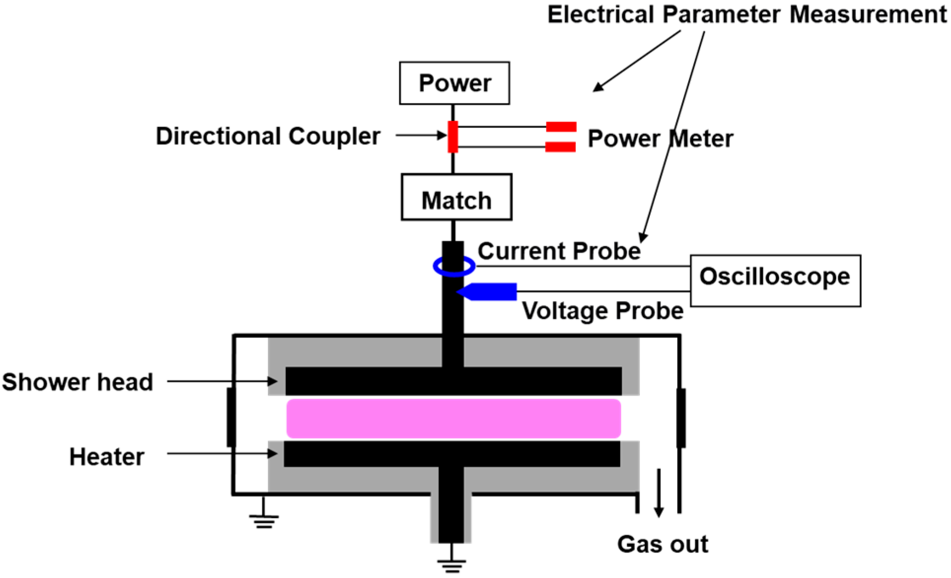
2. Experimental Methods
2.1. Film Deposition
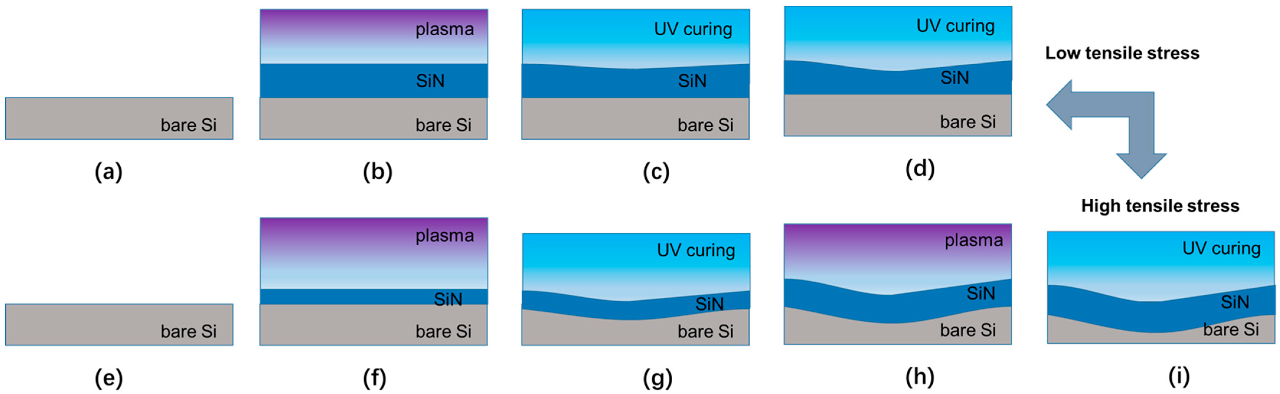
2.2. UV Curing Approach and Layered Deposition
2.3. Characterization Analysis
3. Results and Discussion
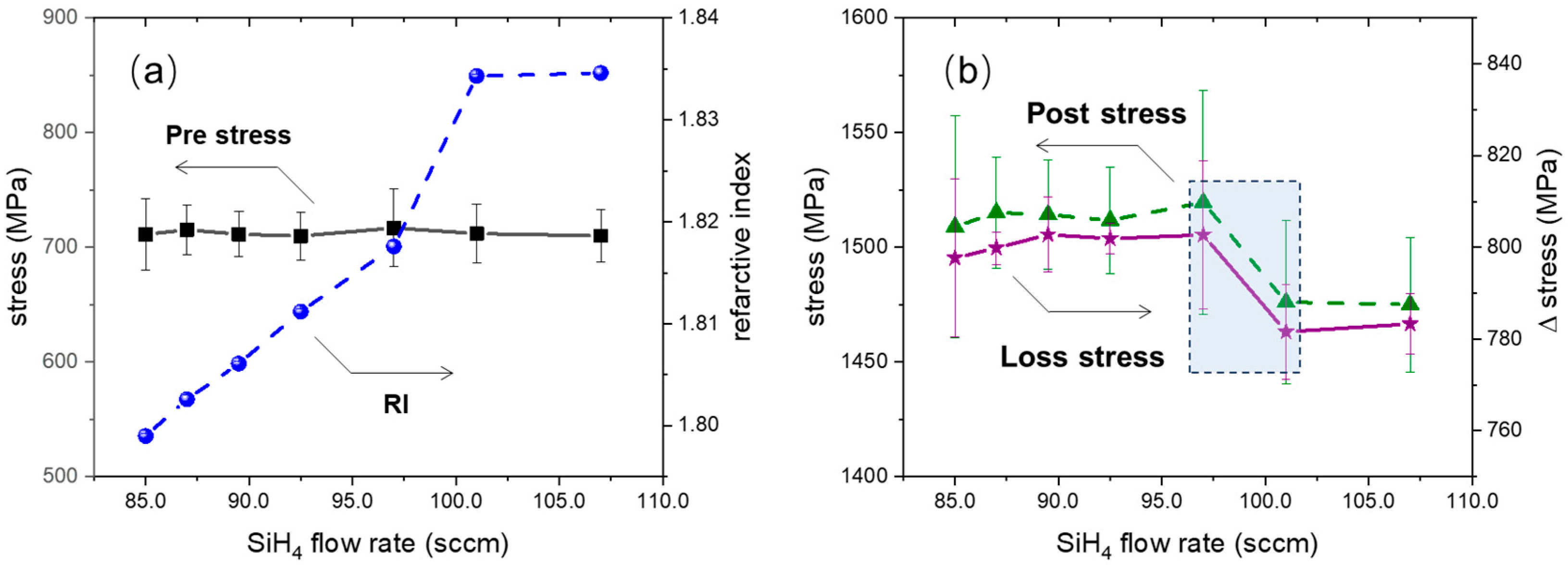
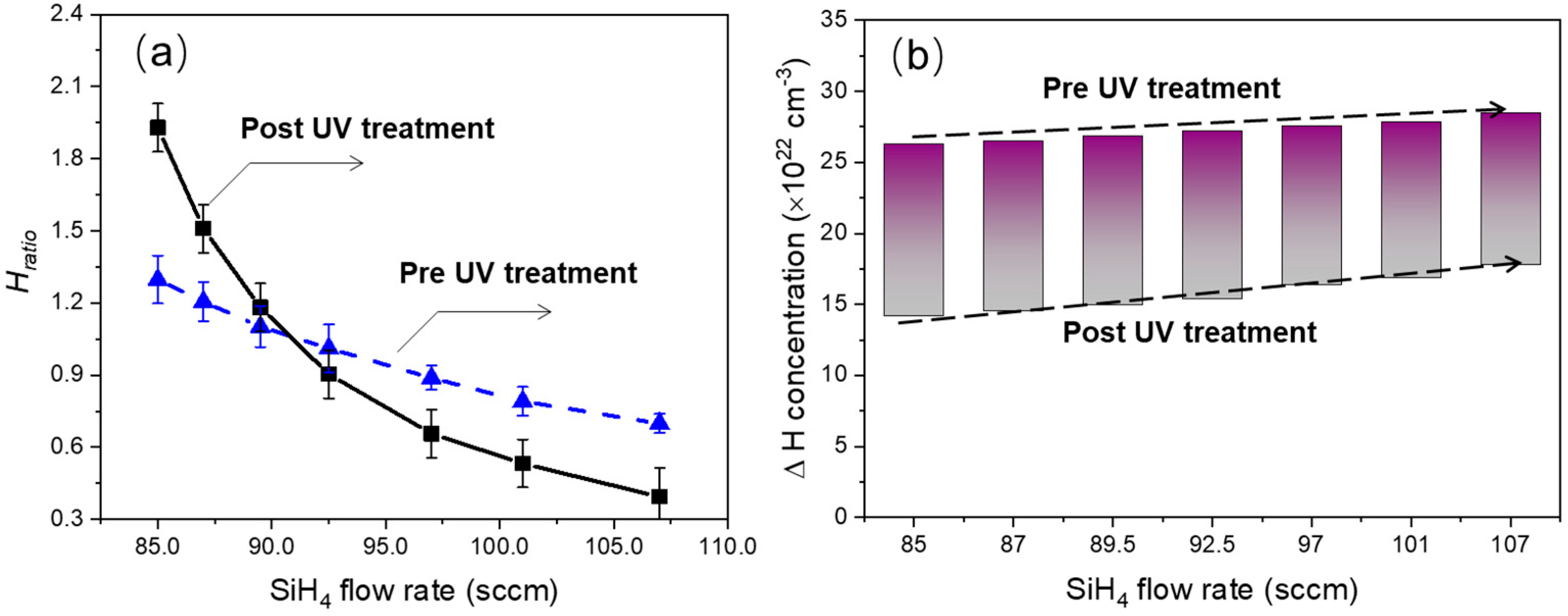
3.1. Low-Tensile-Stress Regime: Effect of PECVD Process Parameters
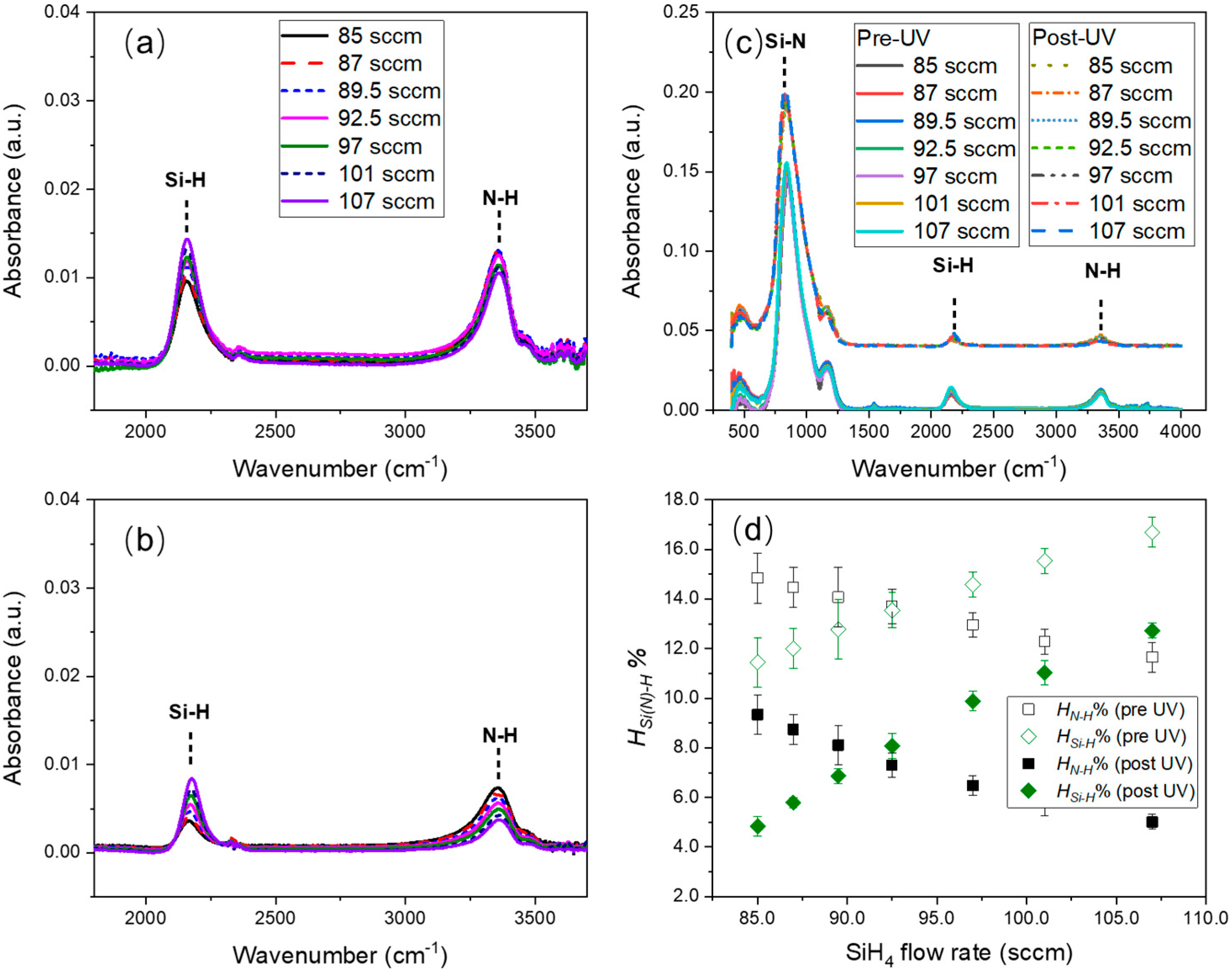
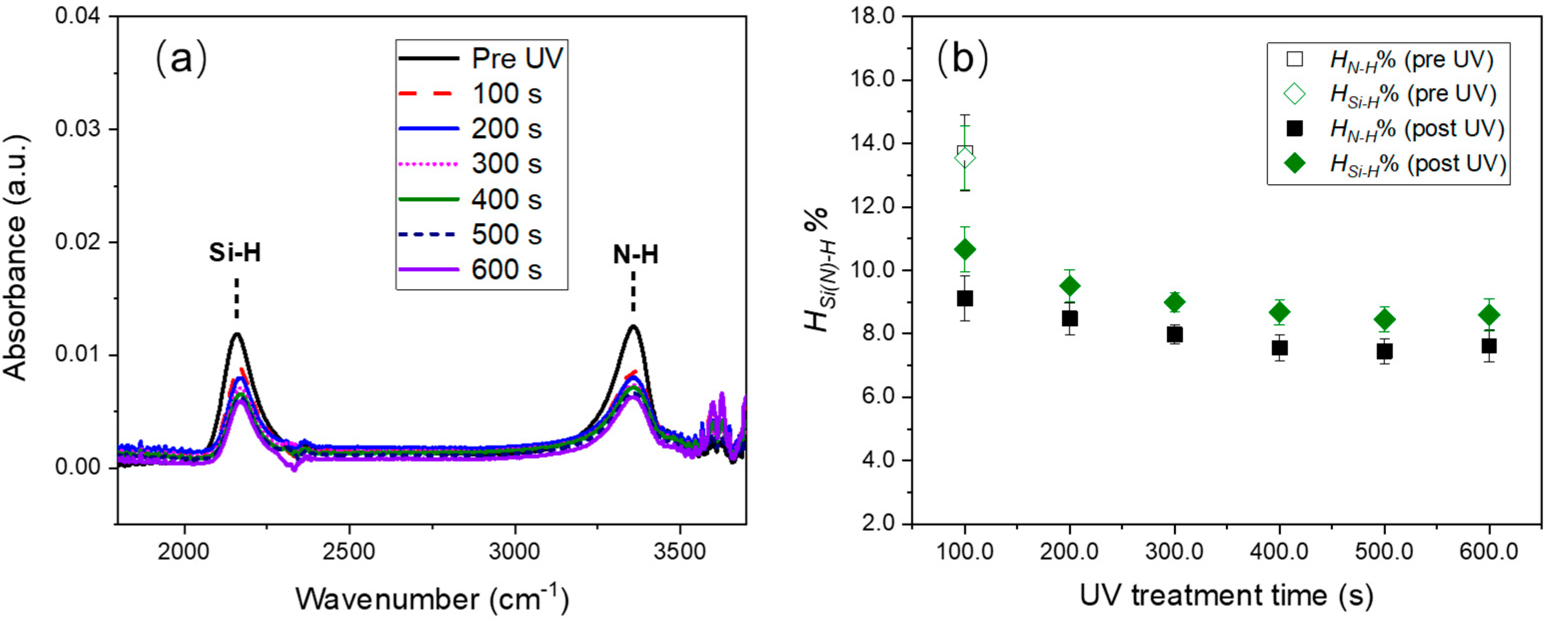
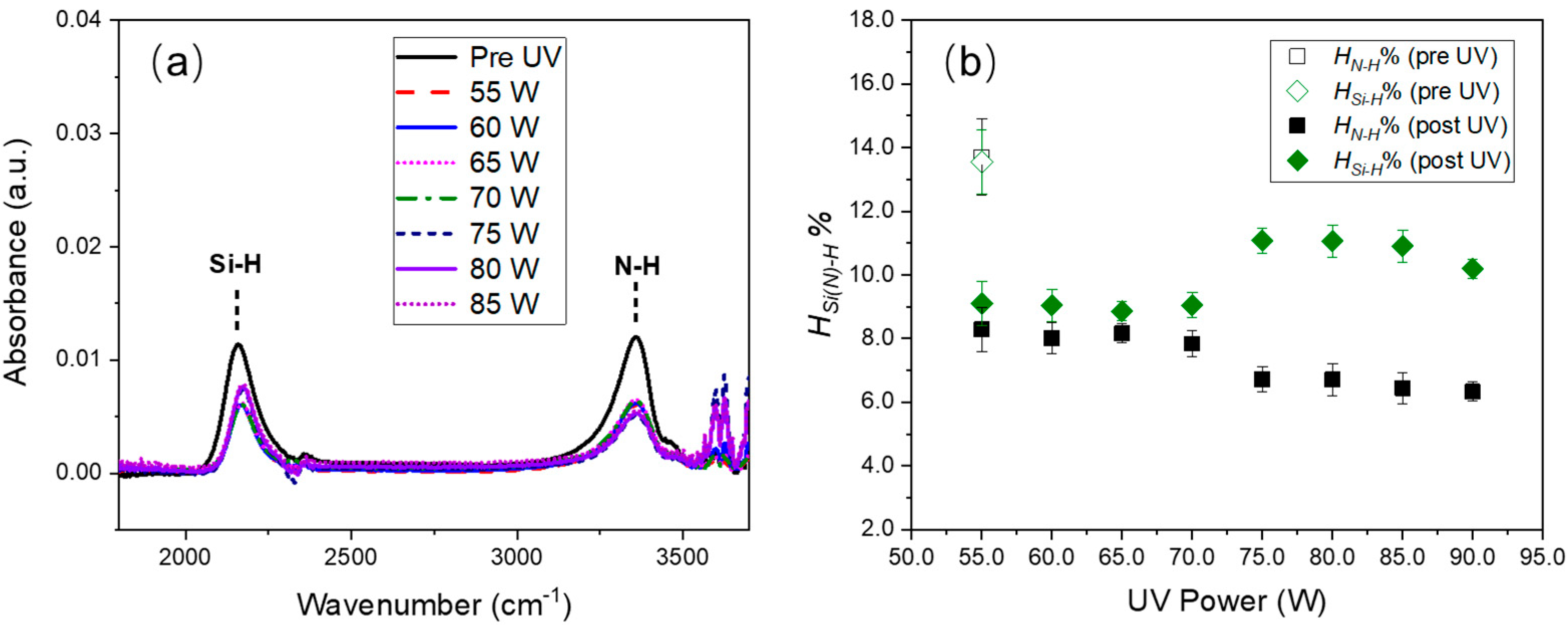
3.2. Low-Tensile-Stress Regime: Effect of UV Curing Parameters
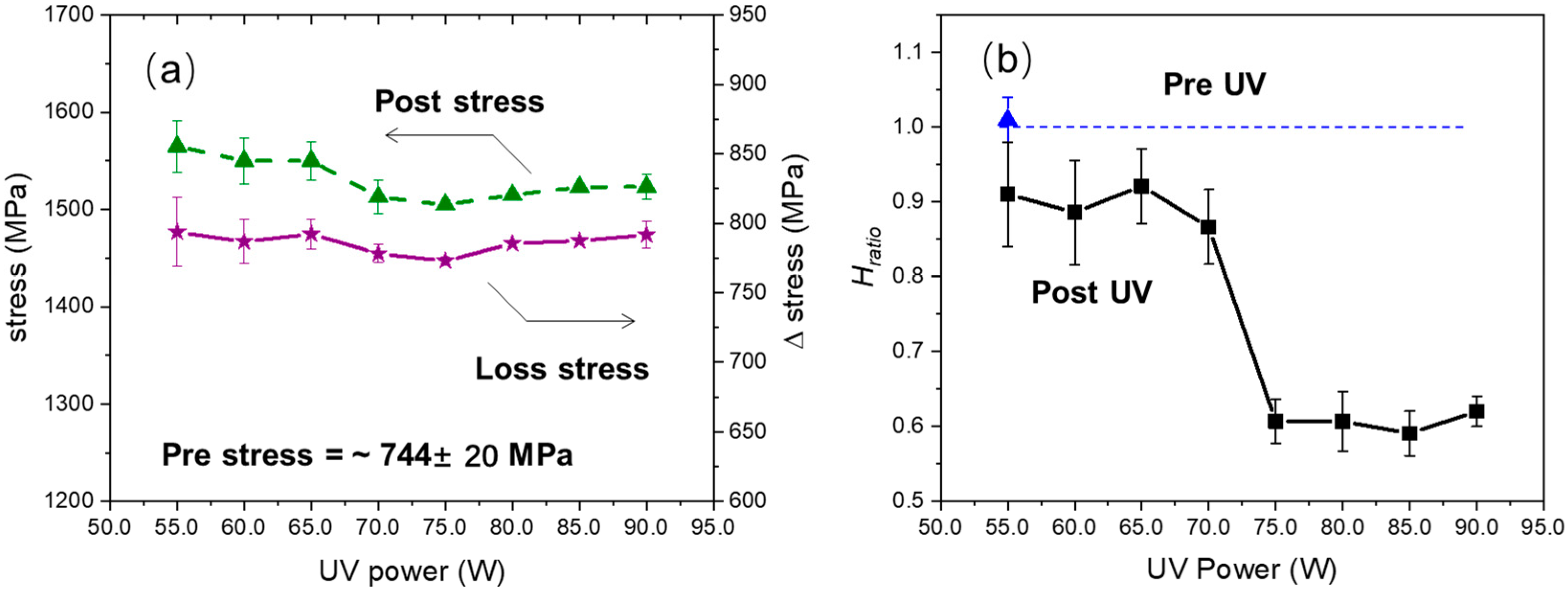
3.3. High-Tensile-Stress Regime: Layered Deposition and UV Curing
4. Conclusions
Author Contributions
Funding
Institutional Review Board Statement
Informed Consent Statement
Data Availability Statement
Conflicts of Interest
References
- Bucher, E.; Fath, P.; Spiegel, M.; Hauser, A. Influence of an ammonia activation prior to the PECVD SiN deposition on the solar cell performance. Sol. Energy Mater. Sol. Cells 2003, 75, 357–362. [Google Scholar]
- Santana, G.; Morales-Acevedo, A. Optimization of PECVD SiN:H “lms for silicon solar cells. Sol. Energy Mater. Sol. Cells 2000, 60, 135–142. [Google Scholar] [CrossRef]
- Chen, Z.; Sana, P.; Salami, J.; Rohatgi, A. A novel and effective antireflection coating PECVD SiO2/SiN for Si Solar Cells. IEEE Trans. Electron Devices 1993, 40, 1161–1165. [Google Scholar] [CrossRef]
- Cho, G.; Cha, H.-Y.; Kim, H. Influence of oxygen–plasma treatment on in-situ SiN/AlGaN/GaN MOSHEMT with PECVD SiO2 gate insulator. Materials 2019, 12, 3968. [Google Scholar] [CrossRef]
- Kim, D.S.; Suh, S.J.; Jang, G.E.; Yoon, D.H.; Yoon, S.G.; Kim, H. Refractive index properties of SiN thin films and fabrication of SiN optical waveguide. J Electroceram 2006, 17, 315–318. [Google Scholar] [CrossRef]
- Eddy, C.R.; Anderson, T.J.; Hobart, K.D.; Kub, F.J.; Koehler, A.D.; Shahin, D.I.; Tadjer, M.J. A Tri-Layer PECVD SiN passivation process for improved AlGaN/GaN HEMT performance. ECS J. Solid State Sci. Technol. 2017, 6, 58–61. [Google Scholar]
- Zhang, L.Q.; Wang, P.F. AlGaN/GaN HEMT with LPCVD deposited SiN and PECVD deposited SiCOH low-k passivation. Appl. Phys. Express 2019, 12, 036501. [Google Scholar] [CrossRef]
- Yang, S.; Ding, Z.Q.; Li, X. Visible to near-infrared light integrated photonic components on PECVD and LPCVD SiN platform. IEEE Photonics J. 2024, 16, 2500207. [Google Scholar] [CrossRef]
- Karunagaran, B.; Suh, E.-K.; Chung, S.; Velumani, S. Effect of rapid thermal annealing on the properties of PECVD SiNx thin films. Mater. Chem. Phys. 2007, 106, 130–133. [Google Scholar] [CrossRef]
- Bellutti, P.; Picciotto, A.; Boscardin, M.; Bagolini, A. Influence of interfaces density and thermal processes on mechanical stress of PECVD silicon nitride. Appl. Surf. Sci. 2009, 256, 215–255. [Google Scholar]
- Chen, K.-C.; Lin, Y.-J.; Huang, P.-C.; Liou, Y.-Y.; Huang, C.-Y.; Chang, C.-P.; Lee, C.-C. Estimated approach development and experimental validation of residual stress-induced warpage under the SiNx PECVD coating process. Surf. Coat. Technol. 2022, 434, 128225. [Google Scholar]
- Lu, C.S.; Lin, H.C.; Huang, T.Y. Impacts of SiN deposition parameters on n-channel metal-oxide-semiconductor field-effect-transistors. Solid-State Electron. 2008, 52, 1584–1588. [Google Scholar] [CrossRef]
- Freund, L.B.; Shin, J.W.; Chason, E.; Hearne, S.J.; Chen, C.-H.; Engwall, A.M.; Miller, C.M. Growth of patterned island arrays to identify origins of thin film stress. J. Appl. Phys. 2014, 115, 123519. [Google Scholar]
- Nix, W.D.; Clemens, B.M. Crystallite coalescence: A mechanism for intrinsic tensile stresses in thin films. J. Mater. Res. 1999, 14, 3467–3473. [Google Scholar] [CrossRef]
- Guisbiers, G.; Overschelde, O.V.; Wautelet, M. Nanoparticulate origin of intrinsic residual stress in thin films. Acta Mater. 2007, 55, 3541–3546. [Google Scholar] [CrossRef]
- Seel, S.C.; Hoyt, J.J.; Webb, E.B. Modeling metallic island coalescence stress via adhesive contact between surfaces. Phys. Rev. B 2006, 73, 245402. [Google Scholar] [CrossRef]
- Chaudhari, P. Grain Growth and Stress Relief in Thin Films. J. Vac. Sci. Technol. A 1972, 9, 520–522. [Google Scholar] [CrossRef]
- Yoneda, M.; Miyagawa, Y.; Murata, T.; Nishida, Y.; Nakai, T.; Hattori, N.; Matsuura, M.; Asai, K.; Uedono, A. Local Bonding Structure of High-Stress Silicon Nitride Film Modified by UV Curing for Strained Silicon Technology beyond 45 nm Node SoC Devices. Jpn. J. Appl. Phys. 2007, 46, 1984–1988. [Google Scholar]
- Lu, C.S.; Lin, H.C.; Huang, T.Y. Optimization of SiN film by varying precursor flow conditions and its impacts on strained channel NMOSFETs. In Proceedings of the IEEE International Conference on Electron Devices and Solid-State Circuits, Tainan, Taiwan, 20–22 December 2007; pp. 117–120. [Google Scholar]
- Yamaguchi, T.; Watanabe, Y.; Hirota, Y.; Hirosawa, I.; Nagata, K.; Son, J.-Y.; Nagasaka, M.; Ogura, A.; Oji, H. Evaluation of stress induced by plasma assisted ALD SiN film. ECS Trans. 2013, 53, 51–56. [Google Scholar]
- Orfert, M.; Richter, K. Plasma enhanced chemical vapor deposition of SiN-films for passivation of three-dimensional substrates. Surf. Coat. Technol. 1999, 116–119, 622–628. [Google Scholar] [CrossRef]
- Subhani, K.N.; Remesh, N.; Niranjan, S.; Raghavan, S.; Muralidharan, R.; Nath, D.N.; Bhat, K.N. Nitrogen rich PECVD silicon nitride for passivation of Si and AlGaN/GaN HEMT devices. Solid-State Electron. 2021, 186, 108188. [Google Scholar] [CrossRef]
- Huang, Y.C.; Chang, S.Y.; Chang, C.H. Effect of residual stresses on mechanical properties and interface adhesion strength of SiN thin films. Thin Solid Film. 2009, 517, 4857–4861. [Google Scholar] [CrossRef]
- Kelm, G.; Jungnickel, G. Hydrogen in plasma-enhanced chemical vapour deposition insulating films. Mater. Sci. Eng. 1991, 139, 401–407. [Google Scholar] [CrossRef]
- Shioya, Y.; Maeda, R.; Kokubun, Y.; Takagi, H. Analysis of stress in plasma enhanced chemical vapor deposition silicon nitride film irradiated with ultraviolet light. Jpn. J. Appl. Phys. 2008, 47, 7081–7088. [Google Scholar] [CrossRef]
- Zhou, D.; Ning, J.; Tang, Z.; Chen, L.; Li, B.; Wu, Q.; Sun, Y. Impact of H-related chemical bonds on physical properties of SiNx:H films deposited via Plasma-Enhanced Chemical Vapor Deposition. Electronics 2024, 13, 2779. [Google Scholar]
- Zhou, M.; Zuo, B.; Tian, J.; Hsia, L.C.; Lu, W. Stress Modulation of Silicon Nitride Film by Initial Deposition Conditions for Transistor Carrier Mobility Enhancement. Jpn. J. Appl. Phys. 2010, 49, 05FB01. [Google Scholar]
- Zubkov, V.; Balseanu, M.; Xia, L.Q. Post deposition ultraviolet treatment of silicon nitride dielectric: Modeling and Experiment. Mater. Res. Soc. 2006, 910, 0910-A19-04. [Google Scholar] [CrossRef]
- Tanaka, T.; Sadoh, T.; Kurosawa, M. Stress-enhancement in free-standing Si pillars through nonequilibrium dehydrogenation in SiN:H stress-liners by ultraviolet light irradiation. Appl. Phys. Lett. 2009, 95, 262103. [Google Scholar] [CrossRef]
- Sadoh, T.; Kurosawa, M.; Heya, A. Enhancement of SiN-induced compressive and tensile strains in Si free-standing microstructures by modulation of SiN network structures. Thin Solid Film 2012, 520, 3276–3278. [Google Scholar] [CrossRef]
- Akazawa, H. Radiation effects in vacuum-ultraviolet-irradiated SiNx: H films. Nucl. Instrum. Methods Phys. Res. B 1996, 116, 355–359. [Google Scholar] [CrossRef]
- Belyansky, M.; Chace, M.; Gluschenkov, O.; Kempisty, J.; Klymko, N.; Madan, A.; Wang, Y.; Yang, D.; Molis, S.; Li, Y.; et al. Methods of producing plasma enhanced chemical vapor deposition silicon nitride thin films with high compressive and tensile stress. J. Vac. Sci. Technol. A 2008, 26, 517–521. [Google Scholar] [CrossRef]
- Auer, I.J.; Meisels, R.; Kuchar, F. Determination of the hydrogen concentration of silicon nitride layers by Fourier transform infrared spectroscopy. Infrared Phys. Technol. 1997, 38, 223–226. [Google Scholar] [CrossRef]
- Maeda, M.; Itsumi, M. Thermal dissociation process of hydrogen atoms in plasma-enhanced chemical vapor deposited silicon nitride films. J. Appl. Phys. 1998, 84, 5243–5247. [Google Scholar] [CrossRef]


| Item | RF Power (W) | RF Frequency (MHz) | T (°C) | Electrode Gap (mm) | SiH4 Flow (sccm) | NH3 Flow (sccm) | N2 Flow (sccm) | Pressure (Torr) |
|---|---|---|---|---|---|---|---|---|
| asic | 175 | 13.56 | 400 | 14.5 | 92.5 | 880 | 2000 | 5.3 |
| SiH4 flow rate | 175 | 13.56 | 400 | 14.5 | 85.0 | 880 | 2000 | 5.3 |
| 87.0 | ||||||||
| 89.5 | ||||||||
| 92.5 | ||||||||
| 97.0 | ||||||||
| 101.0 | ||||||||
| 107.0 |
Disclaimer/Publisher’s Note: The statements, opinions and data contained in all publications are solely those of the individual author(s) and contributor(s) and not of MDPI and/or the editor(s). MDPI and/or the editor(s) disclaim responsibility for any injury to people or property resulting from any ideas, methods, instructions or products referred to in the content. |
© 2025 by the authors. Licensee MDPI, Basel, Switzerland. This article is an open access article distributed under the terms and conditions of the Creative Commons Attribution (CC BY) license (https://creativecommons.org/licenses/by/4.0/).
Share and Cite
Ning, J.; Niu, C.; Tang, Z.; Sun, Y.; Yan, H.; Zhou, D. Optimizing the PECVD Process for Stress-Controlled Silicon Nitride Films: Enhancement of Tensile Stress via UV Curing and Layered Deposition. Coatings 2025, 15, 708. https://doi.org/10.3390/coatings15060708
Ning J, Niu C, Tang Z, Sun Y, Yan H, Zhou D. Optimizing the PECVD Process for Stress-Controlled Silicon Nitride Films: Enhancement of Tensile Stress via UV Curing and Layered Deposition. Coatings. 2025; 15(6):708. https://doi.org/10.3390/coatings15060708
Chicago/Turabian StyleNing, Jianping, Chunjie Niu, Zhen Tang, Yue Sun, Hao Yan, and Dayu Zhou. 2025. "Optimizing the PECVD Process for Stress-Controlled Silicon Nitride Films: Enhancement of Tensile Stress via UV Curing and Layered Deposition" Coatings 15, no. 6: 708. https://doi.org/10.3390/coatings15060708
APA StyleNing, J., Niu, C., Tang, Z., Sun, Y., Yan, H., & Zhou, D. (2025). Optimizing the PECVD Process for Stress-Controlled Silicon Nitride Films: Enhancement of Tensile Stress via UV Curing and Layered Deposition. Coatings, 15(6), 708. https://doi.org/10.3390/coatings15060708