1. Introduction
PZT thin films are widely used in ferroelectric registers and microactuators because of their excellent ferroelectricity and piezoelectricity [
1,
2,
3]. There are many methods for preparing PZT thin films, such as sol–gel, RF sputtering, PLD, and so on. Among them, the RF sputtering method is widely employed due to its high yield, low introduction of impurities, uniform film surface, and small surface roughness [
4,
5].
The performance of PZT depends on many process conditions, such as the sputtering atmosphere, sputtering pressure, annealing temperature, annealing time, and buffer layer, when preparing the films by RF sputtering. Bi et al. [
6] used radio frequency magnetron sputtering to prepare a Pb(Zr
0.52, Ti
0.48)O
3 thin film on a Pt electrode under the deposition parameters of a pure Ar atmosphere, sputtering pressure of 2 Pa, gas flow rate of 24 mL/min, and sputtering power of 40 W. The remaining polarization strength of the film reached 18.7 μC/cm
2, while the coercive field strength was only 28.6 kV/cm, which was successfully applied to ferroelectric film memory. Bose et al. deposited PZT thin films on a Ti substrate and found that the film exhibited tightly packed and uniformly sized grains under a sputtering pressure of 2.9 Pa, and several cracks penetrating the surface could be observed. When the pressure decreased to 0.7 Pa and 0.4 Pa, circular flower garlands of different shapes and sizes (about 0.4–1.2 µm) with a fine particle matrix were observed on the surface of the film. They believe that the circular flower wreath is made of perovskite PZT. Further comparison shows that a sputtering pressure of 0.7 Pa is more favorable for the transformation of PZT thin films into perovskite structures [
7].
A study reported that the change in dielectric constant when O
2/Ar changes is due to the different concentrations of oxygen vacancies in the film [
8]. They accumulate at the grain boundaries because of too many oxygen vacancies, causing the domain wall motion to weaken during polarization, resulting in a decreased dielectric constant. Zhou et al. [
9] pointed out that the leakage current density first decreases and then increases with the increase in O
2/(Ar + O
2). The smallest leakage current density and largest residual polarization are obtained when O
2/(Ar + O
2) is 0.5%, which is different from the optimal O
2/Ar of 0.65/45 reported by Wan et al. [
8]. Bose et al. [
10] reported that PZT films prepared with an O
2/Ar of 1/9 exhibit the highest residual polarization strength of 35 μC/cm
2 and the lowest coercive field strength of 125 kV/cm. The phase purity of the films is affected by the O
2/Ar ratio during sputtering, as reported by Bose et al. [
11]. They believe that the optimal O
2/Ar ratio is 20/80, and PZT films deposited at O
2/Ar ratios of 30/70 or 40/60 exhibit second phases such as PbO, ZrO
2, and pyrochlore structures. Therefore, there is no consensus on the influence of the sputtering atmosphere on the microstructure and electrical properties of PZT thin films.
The formation of pure perovskite PZT films generally requires a transformation process, in which the amorphous film first transforms into the pyrochlore phase at a certain temperature and then transforms into a stable perovskite phase. Bose et al. [
10,
12] mentioned that the transition temperature from the pyrochlore phase (Pb
2(Zr, Ti)
2O
6) to the perovskite phase is approximately 525 °C in sputtered PZT thin films. Frunza et al. [
13] found that the perovskite phase began to appear when the annealing temperature reached 600 °C, and an excellent perovskite phase without residual pyrochlore phase was observed at 650 °C. Nevertheless, Singh et al. argued that the pyrochlore phase occurs when the annealing temperature is below 600. The amount that the pyrochlore phase reduced and the perovskite phase increased corresponded to the increased annealing temperature. It is not until 750 °C that the film is completely transformed into the pure perovskite phase [
14]. Previous studies have shown that the transition temperature from amorphous PZT to the pyrochlore phase and then to the perovskite phase has been controversial. Therefore, further exploration of annealing temperature and time is also a key issue in the preparation of PZT thin films.
In the present study, PZT thin films were deposited on Pt (111)/Ti/SiO2/Si(100) substrates through the RF sputtering method. The influence of the Pb1.2(Zr0.3, Ti0.7)O3 seed layer on the properties of RF-sputtered PZT thin films was compared. Then, the effects of the sputtering parameters and heat treatment parameters on the microstructure, crystal orientation, and electrical properties of PZT films were systematically investigated.
2. Experimental Procedure
2.1. Sample Preparation
In this work, the traditional solid-phase synthesis method was employed to prepare the PZT ceramic target. Pure PbO (99%), ZrO2 (99.5%), and TiO2 (99.5%) powders were weighed according to the stoichiometric ratio of Pb1.1(Zr0.52, Ti0.48)O3 (from China National Pharmaceutical Group Chemical Reagent Co., Ltd., Shanghai, China) and stirred for 3 h using a QM-3SP2 planetary ball mill, in which the 10% excess Pb was added to the targets to compensate for lead volatility. Alcohol was used as the mixing medium. After drying, the mixture was calcined at 800 °C for 2 h in an alumina crucible and ball milled again for 24 h. An amount of polyvinyl alcohol solution was added as a binder after the powder was dried, and the powder was cold pressed in a stainless steel mold. Then, the paste was incubated at 600 °C for 15 min before being coated. The paste was placed in an alumina crucible and calcined for 2 h at 1200 °C. The sintered sample was ground flat on both sides and cleaned to obtain the PZT ceramic target.
PZT thin films were deposited on Pt electrodes using the magnetron sputtering process. Firstly, the SiO
2 layer (1 μm) was formed on a 2-inch Si substrate using the thermal oxidation method. Then, Pt/Ti bottom electrodes of approximately 200 nm were deposited by direct current sputtering. Next, the Pt electrodes were washed in acetone, alcohol, and deionized water for 5 min and then baked on a hot plate to remove moisture before finally being placed on the sputtering chamber stand. After vacuuming to 3.0 × 10
−5 Pa, Ar and O
2 mixed gases (mL/min) were introduced to the chamber using different sputtering atmospheres (O
2/Ar = 0/90, 5/90, 10/90, 15/90, and 25/90) in different experiments. The throttle was adjusted to stabilize the sputtering pressure (0.5 Pa, 2 Pa, 3.5 Pa, and 5 Pa), and then the thin film was deposited. After 2 h, the samples were processed using traditional annealing methods and air atmosphere at different temperatures (525 °C, 550 °C, 575 °C, 600 °C, and 625 °C) as well as times (10 min, 20 min, 30 min, and 40 min). The specific parameters are shown in
Table 1.
2.2. Characterization of Properties
An X-ray diffractometer (D8 Bruker, Bruker, Ettlingen, Germany) at a scanning range of 20–60°, with a step size of 0.02° and a scanning speed of 4°/min, was used to examine the crystal structure of the PZT thin films. The microstructure of the films was characterized using an SU8200 scanning electron microscope (Hitachi, Tokyo, Japan) at a magnification of 120,000 times. Pt top electrodes with a diameter of 1.2 mm were fabricated using direct current sputtering to measure electricity. An impedance analyzer (4294A, Agilent Technologies, Santa Clara, CA, USA) with a frequency range of 0.1 kHz to 100 kHz was employed to measure the dielectric properties of the PZT thin films. Specifically, the capacitance C of the Pt/PZT/Pt structure was first measured at a bias voltage of 1 V, and the loss factor could be directly obtained by the instrument. Then, the effective contact area A, film thickness d, and free space dielectric constant ε0 were combined to obtain the εr of the films (εr = Cd/ε0A). The P-E hysteresis loops were determined by means of a modified Sawyer–Tower circuit.
3. Results and Discussion
We selected an oxygen argon mixture of 5/90 and a sputtering pressure of 1.5 Pa to deposit a seedless PZT film on a Pt electrode, according to
Table 1. Simultaneously, an annealing temperature of 600 °C and an annealing time of 30 min were selected. The XRD diffraction pattern is shown in
Figure 1. The film exhibits a polycrystalline perovskite phase with (100) and (110) preferred, accompanied by some pyrochlore phase. The permittivity (
εr) and loss factors (tan
δ) of the film at a frequency of 0.1 kHz were measured to be 441.2 and 0.351, respectively, indicating poor dielectric properties.
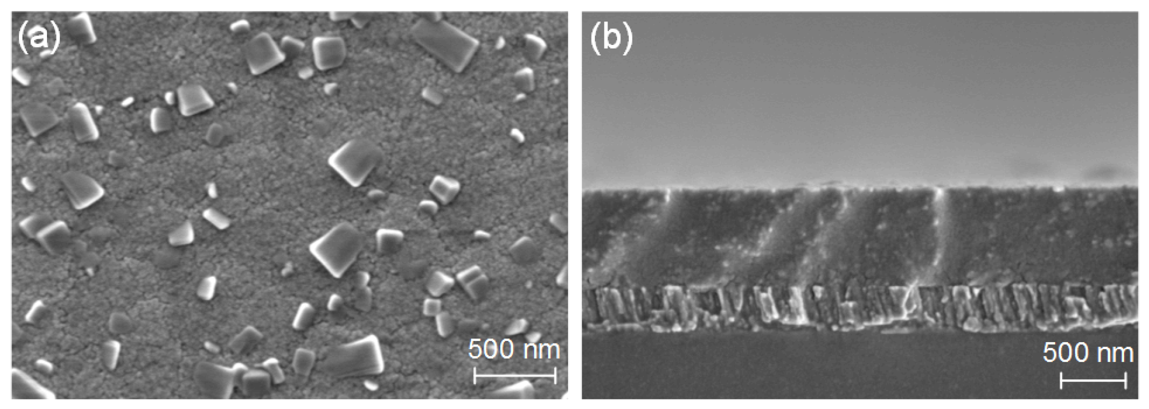
Figure 2 shows the surface and cross-sectional morphology of the seedless PZT film. It can be seen from
Figure 2a that the surface of the film exhibits poor uniformity and smaller grain size, and the grain boundaries are blurred. A large number of precipitation particles with a diameter of about 100 nm appear on the surface. Gong et al. proposed a similar particle as PbO previously [
15]. From the cross-sectional morphology in
Figure 2b, a non-dense film structure with a thickness of 800 nm can also be observed, which is consistent with the XRD results. Kim et al. reported that the crystallization temperature of 650 °C is required for PZT films deposited directly on Pt electrodes, and it is difficult to control the orientation of the film. Polycrystalline-oriented PZT films are even less resistant to the lattice mismatch caused by mismatched thermal expansion coefficients during annealing [
16].
To reduce the lattice mismatch between a PZT film and substrate, a seed layer is usually introduced to enhance the electrical properties of the films [
17,
18]. In this article, a Pb
1.2(Zr
0.30, Ti
0.70)O
3 seed precursor solution was prepared and spin-coated on Pt substrates using the sol–gel method. The deposited films were preheated at 150 °C for 5 min to remove moisture, pyrolyzed at 400 °C for 5 min to eliminate organics, and annealed at 650 °C for 10 min. The above steps were executed several times to obtain a thickness of 100 nm. For ease of description, the seed layer is referred to as Sample 1. Then, the PZT film was deposited on Sample 1 according to the parameters of the seedless PZT film and denoted as Sample 2. The XRD diffraction patterns of Sample 1 and Sample 2 are shown in
Figure 3. It can be observed that both exhibit a (100) preferred orientation, and Sample 2 has a higher degree of (100) orientation, which is ascribed to the guiding role of lead oxide. In fact, PbO appeared on the surface of the films as relatively high amounts of Pb element were introduced to the Pb
1.2(Zr
0.30, Ti
0.70)O
3 seed layer, which provided a good lattice model for the growth of Sample 2 along a (100) orientation [
19]. Sample 2 exhibits a promising
εr of 867 and tan
δ of 0.028, respectively, at a frequency of 1 kHz. Compared with the film without a seed layer, its dielectric properties were significantly improved. The PZT thin films discussed next were all deposited on the Pb
1.2(Zr
0.30, Ti
0.70)O
3 seed layer.
3.1. Effect of Sputtering Atmosphere on Film Properties
We selected a sputtering pressure of 1.5 Pa to deposit the PZT films, as well as an annealing temperature of 600 °C and an annealing time of 30 min. The XRD diffraction patterns of the films deposited in different sputtering atmospheres (O
2/Ar = 0/90, 5/90, 10/90, 15/90, and 25/90) are shown in
Figure 4. It can be noted that all the films exhibit the (100) preferred orientation. Wang et al. reported that post-deposited thin films grow along the substrate orientation when using combination processes (PLD/RF, sol–gel/RF, etc.) to prepare multilayer films [
20]. However, the PZT films in this work exhibit certain differences in crystal orientation with the sputtering atmosphere changes.
Compared to the crystal orientation of the buffer layer, the second phase near 2θ diffraction angles of 36.2°and 53.5°appear in the film with an O
2/Ar of 0/90. Some researchers believe that this is due to the excess Pb pyrochlore phase formed by a pure argon atmosphere [
10]. When the O
2/Ar ratio increases to 5/90, a hump is still observed around 53.5°, which is because the low oxygen content causes oxygen deficiency in the film, resulting in an oxygen-deficient pyrochlore phase [
9]. With the O
2/Ar ratios increasing to 10/90, 15/90, and 25/90, the pure perovskite phase is detected in the PZT films, and the (100) preferred orientation is significantly improved compared with the seed layer. We calculated the (100) orientation degree of all the films. It was found that it first increases and then decreases with the increase in oxygen content, and the maximum orientation degree was obtained at an O
2/Ar ratio of 10/90. As is well known, the phase purity of PZT films depends on many factors, such as target composition, sputtering, and the annealing process. In Bose et al.’s study, the sputtering pressure and substrate temperature were 4.8 Pa and 400 °C, respectively, while they were 1.5 Pa and 25 °C in this research. Therefore, the optimal O
2/Ar ratio is different in this study compared to Bose’s research due to the difference in pressure and substrate temperature during deposition.
3.2. Effect of Sputtering Pressure on Film Properties
We selected an O
2/Ar composition of 10/90 to prepare the PZT films, as well as an annealing temperature of 600 °C and an annealing time of 30 min. The XRD patterns of the films deposited at different sputtering pressures (0.5 Pa, 2 Pa, 3.5 Pa, and 5 Pa) are shown in
Figure 5. It can be seen that PZT films preferentially grow along the (100) direction without the appearance of the pyrochlore phase.
The dielectric properties of the PZT thin films under different sputtering pressures are shown in
Figure 6. It can be inferred from the graph that the
εr and tan
δ of these films first increase and then decrease with the increase in sputtering pressure at a certain frequency. When the sputtering pressure varies within the range of 0.5~3.5 Pa, the
εr changes and reaches its maximum at 2 Pa. With further increasing the sputtering pressure to 5 Pa, the
εr decreases sharply, reaching only 456 at 1 kHz. The XRD and dielectric test results indicate that the most suitable pressure for PZT film preparation is 2 Pa during sputtering.
3.3. Effect of Annealing Temperature on Film Properties
We selected an O
2/Ar composition of 10/90 and a sputtering pressure of 2 Pa to prepare the PZT films, as well as a holding time of 30 min. The XRD patterns of the films were obtained at different annealing temperatures (525 °C, 550 °C, 575 °C, 600 °C, and 625 °C), as shown in
Figure 7. It can be observed that all the films exhibit (100) preferred orientation. The excellent (100) preferred orientation degrees of 75.2% and 73.8% were obtained in the films with annealing temperatures of 575 °C and 600 °C, respectively, which show an increase of 28.9% and 26.7% compared with the 525 °C annealed film. The PZT film with an annealing temperature of 525 °C exhibits a hump near the 2θ angle of 29.2°, indicating the presence of the pyrochlore phase in the film. However, the hump disappears with increasing temperature in the range of 550–625 °C, which means that the PZT films are completely transformed into the perovskite phase. Many studies indicate that PZT films by RF sputtering exhibit the pyrochlore phase under an annealing temperature below 600 °C. Only when the temperature reaches 650–750 °C can films show the pure perovskite phase, and the residual pyrochlore phase is completely eliminated [
13,
14]. Compared with these results, the annealing temperature of 550 °C, at which the PZT film prepared in this work completely transforms into the perovskite phase, is reduced. This may be attributed to the fact that the solid-phase epitaxial effect between the PZT layers deposited by the sol–gel method and RF sputtering decreased the annealing temperature to obtain the perovskite phase during heat treatment, and the same preferred orientation as that of the sol–gel seed layer was obtained [
20].
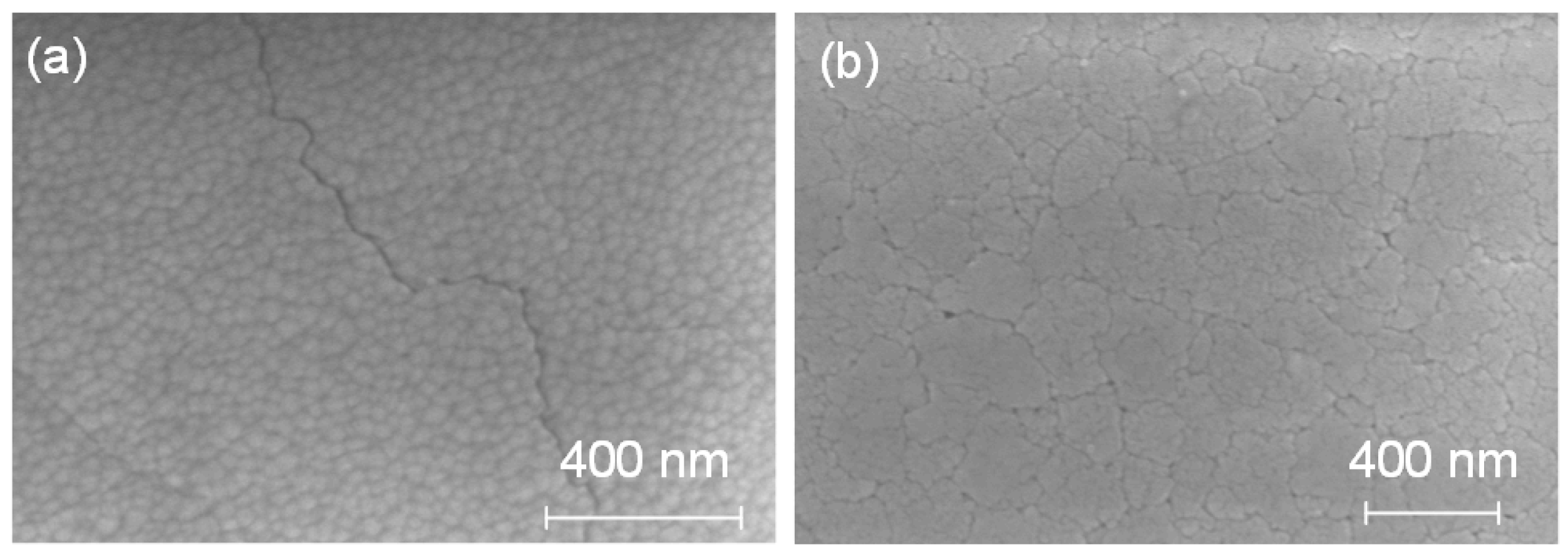
The SEM morphology of PZT films at annealing temperatures of 550 °C and 600 °C is shown in
Figure 8. It can be seen from
Figure 8a that the film surface is flat. The grains are uniform and mostly distributed between 30 and 50 nm, but a few microcracks are exhibited. After annealing at 600 °C, the grain size significantly increased to 200–300 nm, and the surface microcracks disappeared, as shown in
Figure 8b. In fact, the surface morphology of thin films is mainly determined by the annealing temperature on the growth rate and steady-state nucleation rate. Smaller critical nucleation densities and steady-state grain nucleation rates are achieved at lower annealing temperatures, resulting in the formation of small grains. After increasing the annealing temperature, the significant increase in the critical nucleation density and grain nucleation rate promotes the acceleration of grain growth, leading to the formation of large grains.
The variation in
εr with the frequency of PZT films annealed at different temperatures is shown in
Figure 9. It can be observed that the
εr of all films gradually decreases with the increase in frequency, which is ascribed to various polarization factors, such as electrons, ions, and space charges. It is worth noting that the
εr increases first and then decreases with the increase in annealing temperature at a fixed frequency. Optimal permittivity is obtained in the sample annealed at 600 °C, which shows an
εr of 1156 at 1 kHz. The
εr of the film annealed at 525 °C is only 352, mainly due to the deterioration of dielectric properties caused by the presence of the pyrochlore phase inside the film due to the low annealing temperature.
Figure 10 depicts the ferroelectric properties of PZT thin films prepared at different annealing temperatures. For an annealing temperature of 525 °C, the P-E loop of the film shows a significant deviation in the direction of the electric field axis. After increasing the annealing temperature to above 550 °C, promising P-E loops are obtained. An enhanced
Pr (27 μC/cm
2) for the film annealed at 575 °C in comparison to that of 550 °C and 600 °C may be ascribed to the excellent (100) orientation, which decreases the lattice domain switching resistance and improves the movement of domain walls. The film annealed at 600 °C also exhibits larger
Pr (18.5 μC/cm
2) and smaller
Ec (55 kV/cm), and its P-E loop is more symmetrical. It can be seen that the increase in annealing temperature promotes the crystallization of the film, thereby improving its ferroelectric properties.
3.4. Effect of Annealing Time on Film Properties
We selected an O
2/Ar composition of 10/90 and a sputtering pressure of 2 Pa to prepare the PZT films, as well as an annealing temperature of 600 °C.
Figure 11 shows the XRD patterns of the films at different annealing times of 10 min, 20 min, 30 min, and 40 min. It can be observed that all films exhibit a highly (100) preferred orientation, and there is no significant change in the crystal orientation structure and (100) degree with increasing annealing time.
Figure 12 shows the surface morphology of the samples prepared with annealing times of 10 min, 30 min, and 40 min. As is shown in
Figure 12a, unclear grain boundaries, poor film density, small grains, and partial microcracks were demonstrated in the film with an annealing time of 10 min. When the annealing time was increased to 30 min, an improved surface density, more uniform grains, and clear grain boundaries were observed, and the grain size was concentrated between 100 and 200 nm. With increasing the annealing time to 40 min, further increased grain size but decreased compactness were presented. This phenomenon indicates that holding time is particularly important for improving the crystallization properties of the films. There is insufficient time for the film to complete the transformation into the perovskite phase under a short insulation time. However, a longer insulation time promotes the volatilization and diffusion rate of Pb, reducing the surface uniformity of the film. The decreasing uniformity can easily cause an increase in surface stress and cracking of the film, leading to a decrease in the device’s electromechanical coupling ability, deterioration of fatigue performance, and a decrease in stability and reliability. In this work, PZT thin films with moderate grain size and uniform surface morphology were obtained by annealing at 600 °C for 30 min.
The variation in the
εr and tan
δ of the films with frequency at different annealing times is shown in
Figure 13, which indicates that the annealing time has a significant impact on the dielectric properties of the films. For the samples annealed at 10 min and 20 min, the
εr and tan
δ decay rapidly in the low-frequency stage, which is attributed to the presence of more space charges or increased contributions from interface polarization inside the film [
21,
22]. Optimal dielectricity is obtained in the film annealed with 30 min, which presents a permittivity of 852 and a loss factor of 0.026 at a frequency of 1 kHz, respectively. This result is consistent with the microstructure characterization of the film. Therefore, this study believes that PZT thin films annealed for 30 min demonstrate the best dielectric properties.
4. Conclusions
In this study, we prepared PZT thin films with a sol–gel-derived Pb1.2(Zr0.3, Ti0.7)O3 seed layer on Pt/Ti/SiO2/Si substrates using the RF magnetron sputtering method. The dependence of crystal orientation, microstructure, and dielectric behaviors on the sputtering process and heat treatment parameters were investigated. XRD analysis demonstrates the (100) orientation degree of the films first increases and then decreases with the increase in O2/Ar ratios during sputtering, and the mixed phase containing the pyrochlore phase transforms into a pure perovskite phase. The excellent (100) preferred orientation degree of 83.2% is obtained in the film with an O2/Ar ratio of 10/90. The XRD and dielectric test results indicate that the most suitable pressure for PZT film preparation is 2 Pa during sputtering. The pure (100) perovskite phase was detected in the film annealed at a temperature of 550 °C, which indicates that the annealing temperature of the PZT films deposited in this work is reduced. SEM analysis shows that the film processed with an annealing time of 30 min exhibits more uniform grains, clear grain boundaries, and improved surface density. For the film with an O2/Ar composition of 10/90, a sputtering pressure of 2 Pa, an annealing temperature of 600 °C, and a holding time of 30 min, superior dielectricity (εr = 852, tanδ = 0.026) measured at 1 kHz and ferroelectricity (Pr = 18.5 μC/cm2, Ec = 55 kV/cm) were obtained. The experience gained from this work is expected to provide a reference for the preparation of PZT thin films.


