Abstract
The surface quality of high-performance electroformed components, such as the matrix material of the rocket thrust chamber wall, is critical to the overall performance of the devices. However, under high current density and elevated cathode rotation speeds, excessive internal stress often leads to layer detachment, compromising coating adhesion and stability. This study introduces an improved electroforming process termed microbead fusion flexible friction-assisted electroforming (MF3AEF) and examines its effect on the surface roughness of electroformed copper layers. By comparing conventional direct current electroforming (DCEF), abrasive-assisted electroforming (AAEF) with free ceramic beads, and the proposed MF3AEF process, this work investigates the variations in surface quality and roughness under different current densities and cathode rotation speeds. The results indicate that at a current density of 6.8 A/dm2 and a cathode rotation speed of 90 rpm, the surface roughness of the MF3AEF-produced layer is reduced to Ra0.24 µm, representing a 98.2% reduction compared to the Ra13.35 µm achieved by DCEF. This demonstrates that MF3AEF significantly enhances surface properties and markedly reduces the surface roughness of electroformed layers.
1. Introduction
Electroforming is widely employed in industries such as aerospace, computer, pharmaceuticals, and telecommunications to improve hardness, wear resistance, corrosion resistance, surface appearance, and conductivity, among other properties [1,2,3]. However, DCEF sometimes faces limitations with the electroformed layer, including surface defects like pinholes, nodules, coarse-grain structures, and long electroforming cycles. These defects arise due to hydrogen evolution during the electroforming process, where hydrogen bubbles adhere to the cathode, impeding normal metal deposition and resulting in the poor quality of the deposited layer [4]. The surface of the cathode with a complex profile becomes uneven due to the tip effect caused by the electric field distribution [5,6]. To enhance the performance of electroformed layers, researchers have proposed various auxiliary electroforming processes such as ultrasonic-assisted electroforming, magnetic field-assisted electroforming [7], the addition of nanoparticles [8], and composite electroforming [9]. However, nanoparticles tend to poor dispersion and stability in the electroforming solution, which can lead to internal stress and cracks in the electroformed layer [10]. Additionally, composite electroforming processes may exhibit significant variations in particle deposition rates and bonding strengths, affecting the uniformity and performance of the electroformed layer [11,12].
In recent years, flexible friction-assisted electroforming (FFAEF) and AAEF with free ceramic beads have gradually attracted the attention of researchers. Studies have shown that AAEF can effectively eliminate pinholes, remove nodules, improve crystal nucleation, and refine grain size, resulting in near-mirror electroformed layers without the need for organic additives [13,14]. Li et al. [15] provided a novel electroforming technique with an orbital moving cathode, used for the fabrication of non-rotating thin-walled parts. A large number of insulating and insoluble hard particles were added to the electrolyte for real-time polishing of the cathode. Theoretical analysis and experimental results showed that this novel technique could effectively remove the hydrogen bubbles and nodules, disturb the crystal nucleation, and refine the grains of the layer. Zhu et al. [16] employed abrasive-assisted electroforming for revolving parts with complex profiles. A smooth nickel layer with tensile strength 581 MPa, elongation of 17%, and microhardness of 248 HV was obtained. Using a novel abrasive-assisted electroforming technique with free ceramic beads, Hu et al. [17] produced homogeneous nanocrystalline Ni-Co alloys that exhibit an optimal combination of ultrahigh strength, appreciable ductility, and low internal stress. Ren et al. [18] investigated the influences of copper sulfate concentrations and current densities on the tensile properties of free bead-friction-assisted electroforming copper. Low copper sulfate concentrations of 40, 80, and 120 g/L were selected, and ceramic beads were used to grind the surface of the cathode. The results indicated that a reduction in copper sulfate concentration or an increase in current density led to an improvement in both tensile strength and elongation. Lv et al. [19] investigated the influence of various flexible media—such as polymers, bio-bristles, and natural fibers—on the morphology, preferred orientation, and grain size of electrodeposited nickel coatings at varying temperatures. The results revealed that flexible friction effectively inhibits the aggregative growth of adsorbed atoms and removes certain surface-adsorbed species, leading to significant grain refinement and a change in the preferred orientation of the deposits. Shen et al. [20] used flexible friction-assisted jet electrodeposition (FFAJED) and proposed a controllable friction rolling nozzle to study the effect of different current densities on the surface quality of the electroformed layer. Under optimal process conditions, the results revealed a surface free of coarse grains, defects (such as pinholes or nodules), and apparent friction traces.
The foundation of electroforming technology lies in the principle of electrolysis. When a current is applied to the cathode, metal ions precipitate from the electrolyte and deposit on the cathode surface. DCEF is often influenced by uneven current distribution and hydrogen bubble formation, resulting in poor uniformity and density of the electroformed layer. AAEF, which builds on DCEF, involves ceramic beads that grind the cathode surface, refining grains and improving the quality of the electroformed layer. FFAEF, using flexible materials like sponges, provides uniform pressure during electroforming, further enhancing electroformed layer uniformity.
This study proposes an improved microbead fusion flexible friction-assisted electroforming (MF3AEF) process. As shown in Figure 1a, the anode and cathode are filled with hard ceramic during AAFF. However, the arrangement of the anode and cathode machining gaps of MF3AEF is different from the arrangement of AAFF, as shown in Figure 1b. Hard ceramic microbeads are immersed in a flexible sponge, which is located within the gap between the anode and cathode processing. The motor drives the rotation of the cathode core mold, causing the microbeads and sponge to constantly rub and collide with the cathode surface. During the electroforming process, microbeads effectively remove defects such as hydrogen bubbles and nodules on the surface of the electroforming deposit by constantly colliding, squeezing, and grinding the surface of the electroforming deposit. In addition, the movement of microbeads plays a role in shielding the electric field between the cathode and anode. When the electric field is shielded, the grain will stop growing, and after the shield disappears, a new grain will form.
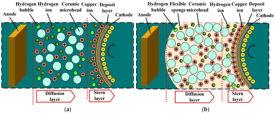
Figure 1.
Schematic diagram of the principle of electroforming: (a) AAEF; (b) MF3AEF.
Through experiments and testing, this study aims to reveal the mechanisms through which MF3AEF enhances the performance of electroformed layers. It is hoped that the results of this study will provide valuable references for the development of electroforming technology and offer new technical means for industrial applications.
2. Experimental Section
2.1. Experimental Setup
For this experiment, a pulse power supply was employed, and the setup is shown in the schematic diagram of the vertical electroforming device in Figure 2. The anode was a copper plate measuring 100 mm × 60 mm × 10 mm. Before the experiment, the anode surface was cleaned of grease and impurities with deionized water and wrapped with a polyester anode bag to prevent the anode sludge produced during the electroforming process from entering the electrolyte and affecting the electroforming results.
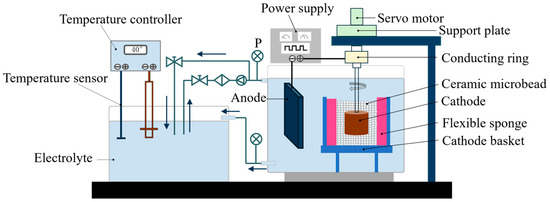
Figure 2.
Schematic diagram of the vertical electroforming setup.
The cathode was manufactured from SUS440 stainless steel, with a rotational diameter of 18.8 mm and a length of 12 mm, as shown in Figure 3a. After cleaning in the ultrasonic cleaning machine, the cathode was wiped with anhydrous ethanol. Finally, the cathode was repeatedly rinsed with deionized water and installed on the vertical lifting device. The cathode basket was made of PVC. The internal diameter, external diameter, and height of the basket were 75, 85, and 130 mm, respectively, as shown in Figure 3b.
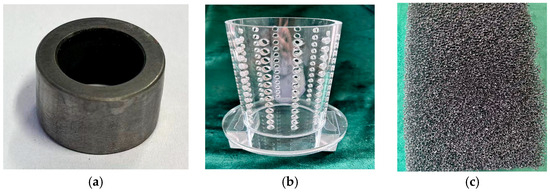
Figure 3.
Physical photographs: (a) the cathode core mold; (b) the cathode basket; (c) thick flexible sponge.
Before the experiment, the cathode basket was placed into the ultrasonic cleaning machine to remove the grease on the surface and then placed into the electroforming tank. A 30 mm thick flexible sponge with 60 PPI (pores per inch), as shown in Figure 3c, was placed in the cathode basket to provide flexible friction and support. Ceramic microbeads with a particle size of 0.8–1.2 mm were filled between the sponge and the cathode. Before the experiment, the microbeads were cleaned with deionized water and then dried. In the electroforming process, the cathode basket and the sponge remain relatively fixed. Microbeads were filled between the cathode and anode and completely covered the surface of the cathode. A speed regulation motor drove the cathode surrounded by ceramic beads to move in self-rotation. Beads moved erratically and ground the surface of the cathode. At the end of the process, the cathode was immediately withdrawn. It was then rinsed with deionized water and dried.
2.2. Electrolyte and Process Conditions
All solutions were prepared using deionized water. The solution content and the experiment condition are shown in Table 1.

Table 1.
Composition of electroforming copper solution and process conditions.
2.3. Performance Testing
The surface morphology and roughness were characterized using a confocal microscope (Germany nanofocus, Oberhausen, Germany), and the final roughness was the average of three measurements. The surface microstructures were investigated by using scanning electron microscopy (SEM; HITACHI SU-8010, Hitachi High-Technologies Corporation, Tokyo, Japan). The phase analysis of the Cu was determined using an X-ray diffractometer (XRD, Bruker D8 Advance, Karlsruhe, Germany).
3. Results and Discussion
3.1. Appearance of Cu Electroformed Layer
From Figure 4, the surface of the copper electroformed layer prepared by DCEF shows a dull and rough texture, with numerous pits and fine specks scattered over the surface. The copper electroformed layer prepared by AAEF, although relatively smooth on the whole, has burrs present in some local areas. However, the copper electroformed layer obtained by M3FAEF is extremely bright, almost attaining a mirror-like reflective effect, and there are no conspicuous macroscopic defects.
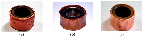
Figure 4.
Appearances of Cu layers: (a) DCEF; (b) AAEF; (c) MF3AEF.
The surface roughness of the copper electroformed layers obtained by both AAEF and MF3AEF techniques is significantly lower than that of traditional copper electroformed layers. This implies that friction-assisted electroforming can effectively enhance the surface quality of electroformed layers, reduce surface defects, and thereby improve surface smoothness. Such enhancements not only beautify the appearance of the copper electroforming layers but may also have a positive influence on their physical and application performance.
3.2. The Effect of Current Density on the Appearance and Surface Roughness
The effect of current density on the surface quality of the electroformed copper layers is significant. Figure 5 and Figure 6 illustrate the effect of current density on the appearance and three-dimensional surface morphology of copper layers produced by various electroforming processes at a cathode rotation speed of 60 rpm. As shown in Figure 5, the AAEF process exhibits an increase in surface roughness with rising current density. Figure 6 reveals analogous trends in MF3AEF, where the surface smoothness decreases as the current density increases. Overall, these findings demonstrate that excessively high current densities can adversely affect the surface quality of the electroformed layer, resulting in increased roughness and reduced brightness.
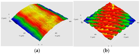
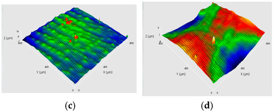
Figure 5.
Digital photographs and 3D surface topographic images of four samples under AAEF with various current densities: (a) 1.7 A/dm−2; (b) 3.4 A/dm−2; (c) 5.1 A/dm−2; (d) 6.8 A/dm−2.
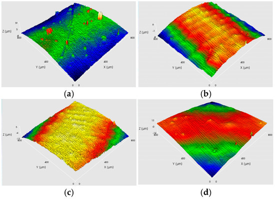
Figure 6.
Digital photographs and 3D surface topographic images of four samples under MF3AEF with various current densities: (a) 1.7 A/dm−2; (b) 3.4 A/dm−2; (c) 5.1 A/dm−2; (d) 6.8 A/dm−2.
As shown in Figure 7, at a rotation speed of 60 rpm, the surface roughness (Ra) of copper layers in traditional electroforming significantly increases from 2.93 µm to 19.07 µm with the increase in current density. Surface defects are induced in DCEF, resulting in increased roughness with high current densities. However, the surface roughness was significantly reduced by AAEF, and the extent of reduction was observed to be greater at higher current densities, with decreases of 61.1%, 85.9%, and 98.2%. Notably, the best surface smoothness and the lowest roughness across all tested current densities are exhibited by the MF3AEF process. Specifically, with a high current density of 6.8 A/dm2, the surface roughness is significantly reduced compared to other processes. A reduction of 98.4% was observed relative to DCEF and 11.8% compared to AAEF.
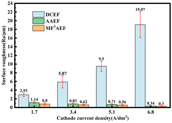
Figure 7.
Surface roughness of copper layers under different processes with different current density.
These phenomena can be attributed to several underlying mechanisms. In the DCEF process, non-uniform current distribution induces internal stress that cannot be effectively released during electrodeposition, leading to disordered grain growth characterized by coarse and uneven grains, which results in peak-valley surface structures and defects such as pinholes, pitting, and nodules. In contrast, the AAEF process utilizes free-moving microbeads that continuously rub and compress the cathode surface, providing smoothing and polishing effects, facilitating hydrogen removal, enhancing mass transfer, and promoting more uniform current distribution. This contributes to grain refinement with finer and more homogeneous grains, although localized stress concentration may still occasionally cause minor surface cracks and fissures.
The MF3AEF process offers a more uniform surface stress distribution, significantly minimizing stress concentration. This contributes to further refinement and homogeneity of the grain structure. The continuous action of flexible microbead friction helps to smooth the surface, improving the uniformity of particle and texture distribution. Consequently, a smooth and flat surface is obtained, with markedly enhanced overall consistency.
Overall, flexible friction-assisted processes significantly improve the surface quality of electroformed copper layers, particularly at high current densities, by substantially reducing surface roughness and enhancing the mechanical properties and durability of the layers.
3.3. The Effect of Cathode Rotation Speed on the Appearance and Surface Roughness
As shown in Figure 8 and Figure 9, at a current density of 6.8 A/dm2, the appearance and 3D surface morphology of copper layers were obtained under different processes by adjusting the cathode rotation speed. According to Figure 8, the copper layer formed using AAEF shows gradual improvement in surface quality as the cathode rotation speed increases from 10 rpm to 60 rpm. At 90 rpm, the surface exhibits more irregularities, indicating possible mechanical or fluid instability. The MF3AEF, as shown in Figure 9, produces copper layers with good surface smoothness across all rotation speeds, especially at 30 rpm and 60 rpm, where the surface roughness is lowest and approaches a mirror-like finish. Although there is a slight increase in roughness at 90 rpm, it remains superior to other processes.
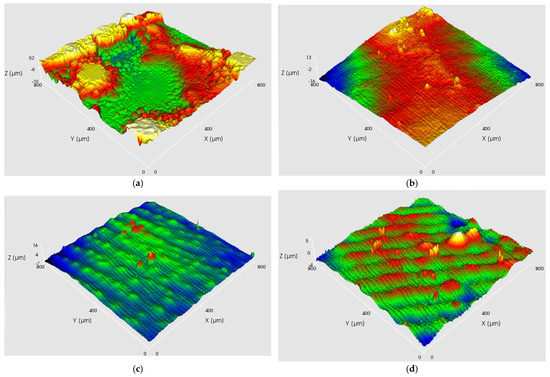
Figure 8.
Digital photographs and 3D surface topographic images of four samples under AAEF with various current densities: (a) 10 rpm; (b) 30 rpm; (c) 60 rpm; (d) 90 rpm.
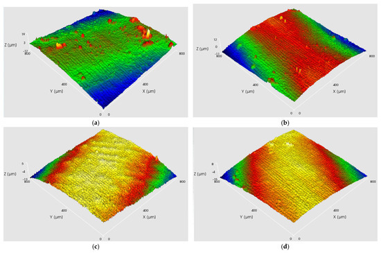
Figure 9.
(a–d) Digital photographs and 3D surface topographic images of four samples under MF3AEF with various current densities: (a) 10 rpm; (b) 30 rpm; (c) 60 rpm; (d) 90 rpm.
At a current density of 6.8 A/dm2, as shown in Figure 10, the surface roughness of copper layers generally decreases with increasing cathode rotation speed across different processes. This indicates that rotation speed positively influences the improvement of copper layer surface quality. Among all rotation speeds, DCEF exhibits the highest surface roughness. Particularly at low rotation speeds, the Ra reaches 26.02 µm, and although it decreases with increasing speed, it remains relatively high. In comparison, AAEF significantly reduces surface roughness, especially at higher rotation speeds. At 90 rpm, the Ra drops to 0.52 µm, highlighting the significant impact of microbead friction in enhancing surface quality. The MF3AEF process consistently shows the best surface smoothness across all speeds, with the lowest surface roughness, particularly at 30 rpm and 90 rpm, where Ra is 0.32 µm. This suggests the MF3AEF technique effectively reduces surface defects, providing excellent surface quality.
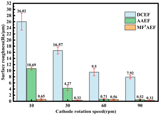
Figure 10.
Surface roughness of copper layers under different processes with different cathode rotation speed.
The observed phenomena can be attributed to the following reasons: increasing the cathode rotation speed enhances convection in the electrolyte. This convection promotes the uniform distribution of ions in the electrolyte, reducing local ion concentration differences and resulting in a more uniform metal layer deposition on the cathode surface. This effect is particularly significant in DCEF processes, where the lack of auxiliary measures leads to greater ion concentration differences. While increasing rotation speed can significantly improve deposition uniformity, the overall effectiveness is still limited. AAEF improves surface quality by physically removing initial deposition defects from the cathode surface, helping to form a smoother metal layer. As the cathode rotation speed increases, the frequency and uniformity of microbead friction improve, further reducing surface roughness. The MF3AEF process utilizes the synergistic effect of flexible materials and microbeads to apply a uniform frictional force on the cathode surface. This approach not only removes initial deposition defects but also prevents the formation of new defects. The elastic cushioning provided by the flexible material accommodates micro-scale surface irregularities, preventing excessive frictional damage. As a result, this process offers the best surface smoothness across all rotation speeds.
In conclusion, the MF3AEF process performs the best in improving the surface roughness of copper layers, with the presence of microbeads being a key factor in achieving this effect. As the rotation speed increases, the surface roughness decreases across all processes, indicating that appropriate mechanical agitation helps enhance the surface quality of the electroformed layers.
3.4. The Influence of Processing Methods on Surface Morphology
As shown in Figure 11, the DCEF sample exhibits a coarse and irregular surface with prominent ridges and uneven grain growth, which is typical under high current density without any auxiliary smoothing mechanism. In contrast, the AAEF sample shows a somewhat improved but still relatively rough morphology due to the limited and uncontrolled abrasive action of free ceramic beads. The MF3AEF sample, however, displays a remarkably smooth and uniform surface with minimal defects and significantly reduced roughness. This dramatic improvement can be attributed to the continuous and flexible friction provided by the microbeads in the MF3AEF process, which effectively removes protrusions in real time, suppresses uncontrolled deposition, promotes grain refinement, and enhances leveling. The mechanical action helps to reduce internal stress and prevent layer detachment, thereby achieving superior surface quality at high current densities and rotation speeds.
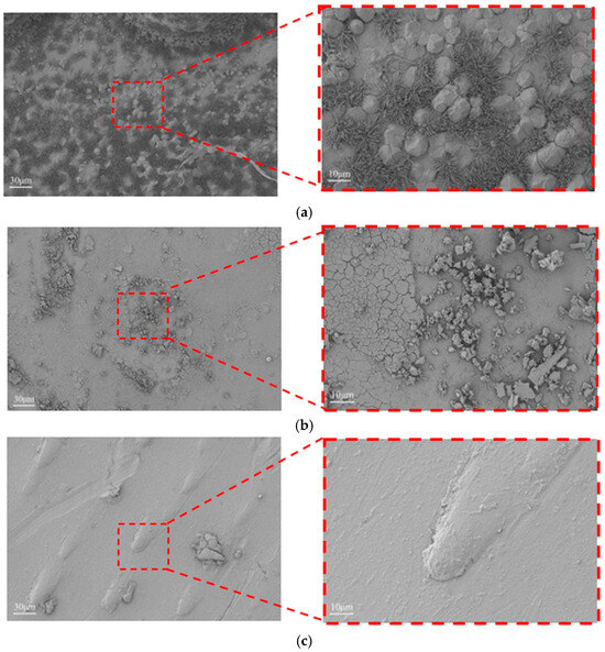
Figure 11.
Surface morphology of copper layers under different processes: (a) DCEF; (b) AAEF; (c) MF3AEF.
Three different electroforming methods were used to compare the crystal phase structures, as shown in Figure 12. Different electroforming methods significantly influence the crystal orientation and phase structure of the electroformed layer. Using DCEF shows relatively weak diffraction peaks, indicating poor crystal orientation and potentially random grain growth. Using AAEF exhibits significantly enhanced Cu(111) and Cu(200) diffraction peaks. This suggests that microbead friction promotes crystal orientation, which helps improve the microstructure of the electroformed layer, making the crystals more likely to grow along these specific crystal planes. Using MF3AEF shows significantly higher intensity of the Cu(220) diffraction peak compared to the other samples, indicating that this method notably enhances the orientation of the Cu(220) plane. The high intensity of the Cu(220) peak suggests that by combining microbeads with flexible friction technology, it is possible to control the grain orientation of the electroformed layer more effectively, promoting preferential crystal growth in a specific direction and thereby improving the crystal quality of the electroformed layer.
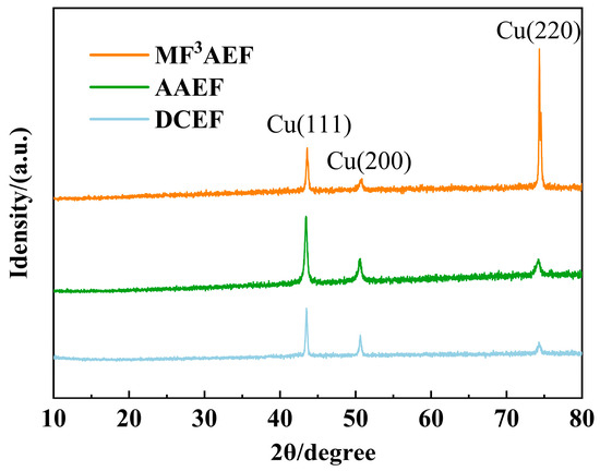
Figure 12.
The X-ray diffraction diagram.
Overall, both AAEF and MF3AEF significantly improved the crystal structure of the electroformed layer. However, the MF3AEF showed superior performance in enhancing crystal orientation and controlling crystal growth. This indicates that incorporating flexible friction and microbead fusion processes plays a significant role in improving the microstructure and overall performance of the electroformed layer, making it a promising approach for high-precision manufacturing applications.
4. Conclusions
In this study, a high-quality surface electroformed copper layer was achieved using the microbead fusion flexible friction-assisted process. The effects of current density and cathode rotation speed on the brightness and surface roughness of the electroformed layer were investigated. The mechanisms by which MF3AEF assists in improving the surface quality of the electroformed layer were also analyzed. The key conclusions are summarized in the following:
- (1).
- The MF3AEF process significantly improved the surface quality of electroformed copper layers. Compared to DCEF, this technology effectively reduced surface roughness, achieving the smoothest surface. This electroforming process showed a particularly notable effect in improving surface quality at high current densities. Under a current density of 6.8 A/dm2 and a cathode rotation speed of 90 rpm, the value of the roughness parameter Ra was reduced to 0.24 µm, representing a 98.20% reduction compared to 13.35 µm in DCEF. This indicates that the MF3AEF is effective in reducing surface defects and enhancing the uniformity of the electroformed layer.
- (2).
- Analysis shows that the MF3AEF process removes hydrogen bubbles that may adhere to the cathode surface through the irregular movement of microbeads in the electroforming solution. This action achieves a more uniform current distribution on the cathode surface, reducing the likelihood of localized high current densities and thus minimizing surface defects such as pits or nodules. Additionally, the flexible friction-assisted component uses materials like sponges to apply a uniform, gentle pressure across the surface of the electroformed layer. Combined with the action of the microbeads, this process mechanically polishes the surface, smoothing out irregularities and eliminating minor defects.
- (3).
- Future research should continue to explore the optimization of process parameters, including the type and size of microbeads and the characteristics of the flexible materials, to further enhance the electroforming outcomes. Specifically, for MF3AEF, optimizing these parameters is expected to further improve the surface quality and mechanical properties of the electroformed layer.
Author Contributions
F.J. conceptualized the methodology, data collection, and data processing for the entire study and wrote the initial draft. S.Q. contributed to the conceptualization and manuscript revision of the research. W.S. performed experiments and analyzed them. Y.K. edited and formatted the paper. All authors have read and agreed to the published version of the manuscript.
Funding
This work was financially supported by the Nantong Science and Technology Project (No: MS2024015).
Institutional Review Board Statement
Not applicable.
Informed Consent Statement
Not applicable.
Data Availability Statement
The original contributions presented in this study are included in the article. Further inquiries can be directed to the corresponding author.
Conflicts of Interest
The authors declare no conflicts of interest regarding the publication of this paper.
References
- Liao, Q.; Li, W.P.; Liu, H.C.; Zhu, L.Q. Fabrication of Nanostructured Electroforming Copper Layer by Means of an Ultrasonic-assisted Mechanical Treatment. Chin. J. Aeronaut. 2010, 23, 599–603. [Google Scholar] [CrossRef]
- Dittmann, R.; Menzel, S.; Waser, R. Nanoionic memristive phenomena in metal oxides: The valence change mechanism. Adv. Phys. 2021, 70, 155–349. [Google Scholar] [CrossRef]
- Lissandrello Magagnin, L. Pulsed electrochemical deposition of calcium phosphate coatings for biomedical applications. Trans. Inst. Met. Finish. 2023, 101, 173–178. [Google Scholar] [CrossRef]
- Ma, Z.; Jiang, B.; Dong, Y.; Qiang, J.; Drummer, D.; Zhang, L. Electrodeposition model with dynamic ion diffusion coefficients for predicting void defects in electroformed microcolumn arrays. Phys. Chem. Chem. Phys. 2023, 25, 7407–7416. [Google Scholar] [CrossRef]
- Rai, P.K.; Biswal, H.J.; Gupta, A. Development of pulse-electroformed Cu/SiC composite tubes with enhanced mechanical and anti-corrosion properties. Arch. Civ. Mech. Eng. 2023, 24, 19. [Google Scholar] [CrossRef]
- Li, A.; Zhu, Z.; Xue, Z.; Liu, Y. Periodic ultrasound-assisted electrodeposition of Fe-Ni alloy foil. Mater. Res. Bull. 2022, 150, 111778. [Google Scholar] [CrossRef]
- Zhai, K.; Du, L.; Wang, W.; Zhu, H.; Zhao, W.; Zhao, W. Research of megasonic electroforming equipment based on the uniformity of electroforming process. Ultrason. Sonochem. 2018, 42, 368–375. [Google Scholar] [CrossRef] [PubMed]
- Weinmann, M.; Jung, A.; Natter, H. Magnetic field-assisted electroforming of complex geometries. J. Solid State Electrochem. 2013, 17, 2721–2729. [Google Scholar] [CrossRef]
- Semboshi, S.; Sakamoto, Y.; Inoue, H.; Iwase, A.; Masahashi, N. Electroforming of oxide-nanoparticle-reinforced copper-matrix composite. J. Mater. Res. 2015, 30, 521–527. [Google Scholar] [CrossRef]
- Evren, B.; Evren, G.; Kıncal, C.; Solak, N.; Ürgen, M. Enhanced interface structure of electroformed copper/diamond composites for thermal management applications. Mater. Test. 2024, 66, 422–432. [Google Scholar] [CrossRef]
- Walsh, F.C.; de Leon, C.P.; Bavykin, D.V.; Low, C.T.J.; Wang, S.C.; Larson, C. The formation of nanostructured surfaces by electrochemical techniques: A range of emerging surface finishes-Part 1: Achieving nanostructured surfaces by electrochemical techniques. Trans. Inst. Met. Finish. 2015, 93, 209–224. [Google Scholar] [CrossRef]
- Zhang, H.; Zhang, N.; Gilchrist, M.D.; Fang, F. Advances in precision micro/nano-electroforming: A state-of-the-art review. J. Micromech. Microeng. 2020, 30, 103002. [Google Scholar] [CrossRef]
- Zhu, Z.-W.; Zhu, D.; Qu, N.-S.; Wang, K.; Yang, J.-M. Electroforming of revolving parts with near-polished surface and uniform thickness. Int. J. Adv. Manuf. Technol. 2008, 39, 1164–1170. [Google Scholar] [CrossRef]
- Lin, J.; Kilani, M.; Baharfar, M.; Wang, R.; Mao, G. Understanding the nanoscale phenomena of nucleation and crystal growth in electrodeposition. Nanoscale 2024, 16, 19564–19588. [Google Scholar] [CrossRef] [PubMed]
- Li, X.; Zhu, Z.; Zhu, D.; Zhang, Y. Orbital-abrasion-assisted Electroforming of Non-rotating Parts. J. Wuhan Univ. Technol.-Mater. Sci. Ed. 2011, 26, 827–831. [Google Scholar] [CrossRef]
- Ren, J.H.; Zhu, Z.W.; Zhu, D. Effects of process parameters on mechanical properties of abrasive-assisted electroformed nickel. Chin. J. Aeronaut. 2016, 29, 1096–1102. [Google Scholar] [CrossRef][Green Version]
- Hu, J.C.; Zhu, Z.W. Homogeneous nanocrystalline Ni-Co alloys with excellent mechanical properties via abrasive-assisted electroforming. J. Mater. Sci. 2023, 58, 9349–9361. [Google Scholar] [CrossRef]
- Yin, G.; Ren, J.; Wang, Z.; Yao, C.; Dong, Y.; Zhou, C. Investigation of the Tensile Properties of Friction-Assisted Electroforming Copper with Free Beads. J. Mater. Eng. Perform. 2023, 33, 9676–9685. [Google Scholar] [CrossRef]
- Lv, B.; Hu, Z.; Wang, X.; Xu, B. Electrodeposition of nanocrystalline nickel assisted by flexible friction from an additive-free Watts bath. Surf. Coat. Technol. 2015, 270, 123–131. [Google Scholar] [CrossRef]
- Liu, X.; Shen, L.; Qiu, M.; Tian, Z.; Wang, Y.; Zhao, K. Jet electrodeposition of nanocrystalline nickel assisted by controllable friction. Surf. Coat. Technol. 2016, 305, 231–240. [Google Scholar] [CrossRef]
Disclaimer/Publisher’s Note: The statements, opinions and data contained in all publications are solely those of the individual author(s) and contributor(s) and not of MDPI and/or the editor(s). MDPI and/or the editor(s) disclaim responsibility for any injury to people or property resulting from any ideas, methods, instructions or products referred to in the content. |
© 2025 by the authors. Licensee MDPI, Basel, Switzerland. This article is an open access article distributed under the terms and conditions of the Creative Commons Attribution (CC BY) license (https://creativecommons.org/licenses/by/4.0/).