Article

Environmentally Durable Au-Based Low-e Coatings

by
Wan Noor Sofia Wan Shamsuddin
*,
Kamil Zuber
,
Peter J. Murphy
and
Marta Llusca Jane
*
Materials Engineering Group, Future Industries Institute, University of South Australia, Adelaide 5095, Australia
*
Authors to whom correspondence should be addressed.
Coatings 2025, 15(10), 1231; https://doi.org/10.3390/coatings15101231
Submission received: 26 September 2025 / Revised: 16 October 2025 / Accepted: 16 October 2025 / Published: 21 October 2025
(This article belongs to the Special Issue Novel Research on Optical Materials and Coatings)

Abstract

Low-emissivity (low-e) coatings are used in architectural and automotive glazing for energy-saving applications. These are used to minimise heat transmission through the windows by reflection. Low-e coatings are semi-transparent coatings that typically comprise a metallic layer that reflects infrared light, sandwiched between two dielectric layers that protect the metal and enhance its visible transmittance. Ag is usually used as the metallic layer because of its colour neutrality and low optical absorption in the visible range. However, Ag-based low-e coatings easily degrade upon atmosphere exposure; therefore, they need to be placed inside the cavities of multiple-pane windows. In this paper, Au was used as an alternative to Ag and was sandwiched between WO3, SnO2 and Nb2O5 dielectric layers. The thickness of each layer was optimised to achieve the highest visible transmittance and infrared reflectance. The durability of the coatings was assessed by means of corrosion and abrasion resistance tests. We demonstrate that the Nb2O5/Au/Nb2O5 coating system provides a visible light transmittance of 56%, an emissivity as low as 0.04 and outstanding corrosion resistance (1000 h of salt spray testing), indicating its excellent potential to be used as first surface low-e coating.

1. Introduction

Low-emissivity (low-e) coatings are generally used in energy-saving windows to reduce electricity consumption and improve comfort when air-conditioning or heating is required. These coatings allow the visible light of the solar spectrum to go through but reflect infrared (IR) radiation [1,2]. Low-e coatings consist of a multilayer system, in which metallic (M) and dielectric (D) layers are combined in a DMD configuration (as shown in Figure 1). The metallic layer is responsible for reflecting IR radiation and needs to be thin enough (typically 10–20 nm) to be visually transparent. The dielectric layers (approximately 40 nm thick) are used to improve the visible light transmittance and protect the metallic layer from environmental degradation [2,3,4,5]. The metallic layers are comprised of high-electrical-conductivity metals, such as Ag, Cu or Au. Ag has arguably been the most often used because of its low absorption in the visible range, high conductivity and colour neutrality (blue hue rather than yellow) [2,3,6,7,8,9,10,11,12]. Dielectrics that are typically employed in DMD structures are WO3, SiO2, ZnO and SnO2, amongst others, which, when combined with Ag, have been proven to achieve high-visible transmittance and high infrared reflectance [3,13,14]. A major disadvantage of Ag is that it tarnishes very easily upon atmosphere exposure. For example, Ross et al. [15] demonstrated that Ag-based low-e coatings formed white casts when exposed to humidity, and Ando et al. [16] reported on interfacial adhesion issues in ZnO/Ag/ZnO coatings because of Ag interface migration. Shamsuddin et al. [17] also showed white cast and adhesion issues on TiO2/Ag/Ti/TiO2 low-e coatings after long exposure in a salt spray corrosion chamber.
An alternative to Ag in low-e coatings is Au, which exhibits higher electrical conductivity and higher environmental stability. However, Au thin films present a reflectance peak in the visible region (520 nm) [18], contributing to the gold colour [19]. Some authors [20] have combined Au with Bi2O3 and SiO2 in DMD systems, resulting in visible transmittances of 73% and 68%, respectively, at 560 nm. Al-Kuhaili et al. [21], for example, also presented a study on thermal evaporated WO3 (34 nm)/Au (36 nm)/WO3 (34 nm), which provided a maximum transmittance of 84% at 680 nm. The same authors [18] reported a comparison of the optical properties of different Au-based bi-layer systems (glass substrate/Au/D), theoretically and experimentally, using 10 different dielectrics. The best bi-layer system found was WO3 (32 nm)/Au (17.6 nm), which exhibited 69.4% reflectance in the infrared range and 65.7% transmittance at 564 nm [22]. To the best of the authors’ knowledge, the environmental durability of Au-based low-e coatings has not yet been reported in the literature [23]. Therefore, a key novelty of the present study lies in the evaluation of the environmental stability and durability of Au-based low-e coatings, providing valuable insight into their potential for long-term practical applications.
In general, low-e coatings are fabricated on glass substrates, but more recently, in the architectural and automotive sectors there is growing demand to use plastic-based substrates due to their lightweight and flexibile design [24], particularly in the case of flexible films that use roll-to-roll fabrication processes. To date, only a few studies have been published on the development of low-e coatings on polymer-based substrates [17,25].
In this study, Au was investigated as a potential metallic layer with three different dielectrics, WO3, Nb2O5 and SnO2, in DMD systems on polymeric substrates. The thickness of the metallic and dielectric layers was varied to achieve maximum transmittance in the visible range and maximum reflectance in the IR region. To improve the corrosion and abrasion resistance, the need for a transparent hard-coat resin on top of the DMD systems is discussed in detail. This study demonstrates the potential of Nb2O5/Au/Nb2O5 as a weather-resistant low-e coating, as proven by the optical and corrosion resistance characterization. This robust and simple coating design exhibits an excellent choice over Ag-based low-e coatings and opens up the possibility of being used in flexible plastic films.

2. Experimental Procedure

2.1. Sample Preparation

Au-based low-e coatings (Nb2O5/Au/Nb2O5, WO3/Au/WO3, SnO2/Au/SnO2) were sputter-deposited on commercial hard-coated polycarbonate (PC), Makrolon AR, from Bayer MaterialScience, Germany (7 × 7 × 0.4 cm). The PC substrates were cleaned thoroughly for 6 min in an ultrasonic bath in OP164 detergent from Deconex and deionised water (ratio 3:97), then rinsed with deionised water and dried using compressed air. Before the sputter deposition, the substrates were further treated with RF air plasma in a Diener Electronic plasma surface treatment machine for 2 min. The coatings were deposited in a Direct Current (DC) magnetron sputtering system, which was evacuated to 1.3 × 10⁻⁶ mbar base pressure prior to deposition. The pure Au metallic coating was deposited with the assistance of Ar gas, while the dielectric layers were deposited from respective metallic targets through reactive sputtering, with oxygen gas added during deposition. All the targets were 99.99% pure and supplied by Plasmaterials, USA. The deposition parameters for each of the layers can be seen in Table 1.
The deposition of Au, WO3 and SnO2 was performed using 3-inch-diameter magnetron targets of Au, W and Sn. The substrates were placed 12 cm from the target on a rotary stage that rotated at 20 rpm during deposition to produce a uniform coating. The deposition of Nb2O5 films was performed with the substrate rotated at 40 rpm and positioned at 15 cm from the target. The Nb target was rectangular and measured 12.7 × 30.5 cm.
Some of the Au-based multilayer coatings (as described further in the manuscript) were additionally protected with 10 nm of SiO2 and a 5 µm thick transparent hard coat (HC) resin. The SiO2 film acted as an adhesion layer to promote the adhesion of the multilayer coating to the HC. These SiO2 films were deposited in a custom-made inline sputtering system from a rotatable cylindrical Si target (80 cm in height and 7.5 cm in diameter). In this case, the speed of the substrate carrier determined the thickness of the films.
A transparent hard-coat resin, CrystalCoat MP101 from SDC Technologies, USA (solid content 32.5%), was dip-coated onto the DMD coating system with SiO2 as an adhesion layer. The dip coater used for this process was the Qualtech QPI-168, Canada and the coating was performed at a withdrawal rate of 500 mm/min, which resulted in a thickness of 5 µm. After dip-coating, the samples were hung vertically in a fume cupboard for 20 min at controlled humidity of 25–30% to evaporate the solvents, and then cured in an oven at 130 °C for 1 h.

2.2. Sample Characterisation

2.2.1. Optical and Electrical Properties

A Cary 5000 spectrophotometer from Agilent Technologies, CA, USA was used to measure the transmittance and reflectance of the samples in the range from 380 nm to 3300 nm. The visible solar-weighted transmittance (Tvis) and the infrared solar-weighted reflectance (RIR) were calculated as per Equations (1) and (2), respectively.
T V I S = 380 780 % T · I d λ I d λ · 100
R I R = 785 3300 % R · I d λ I d λ · 100
where I is the solar irradiance, and dλ is the wavelength interval of integration.
High Tvis and high RIR are equally important in determining an optically efficient low-e coating. To assess the best thickness combination of materials, a Figure of Merit (Φ) was calculated as per Equation (3). The higher the Φ, the more optically efficient the low-e coating.
Φ = T v i s · R I R 100
A CIE L*a*b* coordinate system with a D65/10 standard illuminant/observer was utilised to evaluate the colour of the coatings. The colours were quantified with L*, a* and b* parameters, which denote luminescence, green/red colour and blue/yellow colour, respectively. These values were extracted from the transmittance measurement performed with the Hunterlab (VA, USA) UltraScan Pro spectrophotometer between 380 nm and 1050 nm.
The conductivity ( σ ) of the samples was calculated using the sheet resistance ( R s ), which was measured with a RM3 4-point probe, from Jandel Engineering, UK, at 1 mA constant current flow. The σ , in S·cm−1, was calculated as follow Equation (4):
σ = 1 R s · t · 10 7
where R s is in Ω/□, and t is the coating thickness in nm.
The emissivity (ε) of the coating was measured with a FLIR E75 thermal camera, OR, USA as per the FLIR manual. The samples were heated on a hot plate at 70 °C, together with black electrical tape with a known emissivity of ε = 0.97. The tape was then imaged through the thermal camera, and its temperature was measured at the control emissivity ε = 0.97. Then, the camera was used to image the sample surface, and the emissivity setting was adjusted until the camera measured the same temperature as the tape. The emissivity recorded corresponds to the emissivity of the sample.

2.2.2. Morphology

The thickness of the films was measured with a Bruker (Germany) Dektak XT Stylus profilometer.
The surface morphology was analysed using an Atomic Force Microscope (AFM) from Bruker Multimode 8. The images were taken in tapping mode using a tip from Budget Sensors, Bulgaria (f = 300 kHz, k = 40 N/m). The images were analysed using the Gwyddion software, Version 2.60. to calculate the root mean square roughness (RRMS) values of the films.

2.2.3. Abrasion Resistance and Adhesion

Bayer and Steel Wool tests were employed to assess the abrasion resistance of the samples. The Bayer test was performed using a Taber Oscillating Abrasion Tester (Model 6100), NY, USA as per the ASTM F735 standard. The coated samples were loaded in a tray, with 500 gr of alundum chips, which moved back and forth for 300 cycles at a speed of 2.5 cycles/second. A Sutherland Rub Tester 2000 (Danilee Co, OH, USA) instrument was employed to conduct the Steel Wool test. The test was performed using grade 0 steel wool at a load of 2 kg for 3 sets of 25 cycles at a speed of 0.7 cycles/second with 1 min pauses between the cycles. To evaluate the damage to the coating after both tests, the samples were visually inspected, and the transmitted haze before and after the tests (∆H%) was measured using the Hunterlab (VA, USA) UltraScan Pro spectrophotometer. The lower the ∆H%, the more abrasion-resistant the sample.
The adhesion of the coatings to the substrate was evaluated using the cross-hatch tape test according to ASTM D3359-09e2. The coating was cross-cut with a sharp blade and covered with 3M (MN, USA) Scotch 600 tape for 1 min. The tape was then removed, and the cross-hatch pattern was visually inspected and rated on a scale from 0B (more than 65% delamination) to 5B (no coating removed).

2.2.4. Corrosion Resistance

A salt spray chamber from Ascott was used to expose WO3/Au/WO3, SnO2/Au/SnO2 and Nb2O5/Au/Nb2O5 samples with and without HC to salt spray (5% NaCl solution) at a pH of 6.5–7.5 at 35 °C (as per the ASTM B117-18 standard). The tested samples were monitored regularly by measuring the change in the optical properties (ΔTVIS and ΔRIR) with a Cary 5000 spectrophotometer (Agilent Technologies, CA, USA). Surface changes were also observed through an Olympus (Japan) SC 50 optical microscope. A pass criterion was applied if the samples showed no visual changes after 1000 h of testing (the criterion used in the automotive industry for exterior components).

3. Results and Discussion

3.1. Optical Analysis

WO3, SnO2 and Nb2O5 were selected as the dielectric layers because of their low absorption, high transmittance in the visible, and high refractive index [3,26]. For application in low-e coatings, dielectrics with a refractive index of at least 1.96 are recommended [3,27].
To maximize the optical performance (high Tvis, high RIR) of the different DMD systems, the thickness of each layer was varied around previously reported optimum thicknesses in similar systems, which are 10–45 nm for metal, and 30–60 nm for the dielectric layers [3]. Firstly, the thickness of Au was varied while keeping the dielectric thickness constant at 40 nm, and then the Au thickness was kept constant while varying the thickness of the dielectric layer. A Figure of Merit (Փ) was used to consider both high Tvis and high RIR for each multilayer design (Equation (3)). The higher the Փ, the higher the overall optical performance of the low-e coating.

3.1.1. Metallic Layer

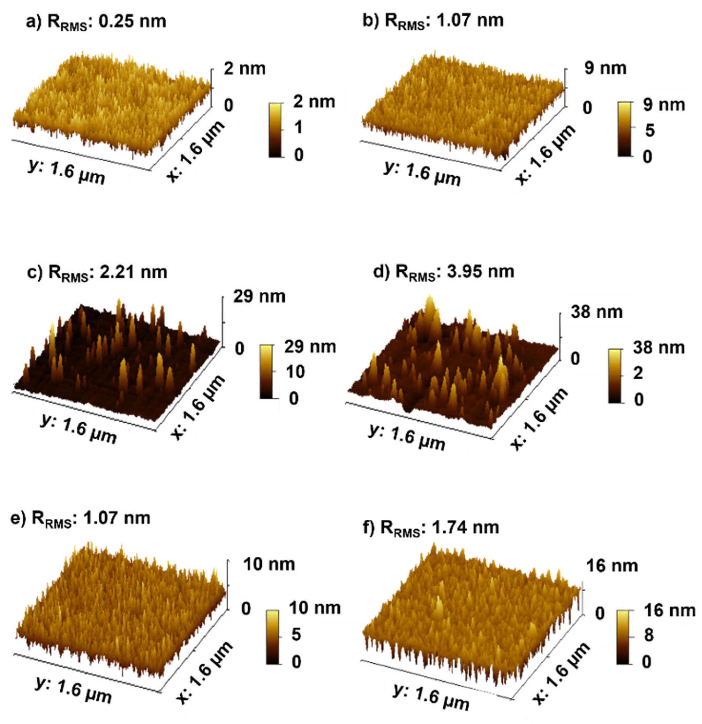
DMD coatings were fabricated with 40 nm thick WO3, SnO2 and Nb2O5 dielectric layers, and the thickness of Au was varied from 10 to 45 nm. The resultant optical properties of the DMD systems, summarised in Table 2, demonstrate that the thicker the Au film, the lower the TVIS and the higher the RIR, which is in agreement with Beer’s law. The optimum thickness values for Au, as determined by Փ, were 15, 40 and 20 nm for WO3, SnO2 and Nb2O5, respectively. Although 15 to 20 nm of Au was sufficient to provide high Tvis and RIR (Փ > 0.4) for WO3 and Nb2O5, respectively, SnO2 required at least 40 nm to achieve similar values (Փ > 0.38). To further understand such behaviour, the surface morphology of 40 nm thick WO3, SnO2 and Nb2O5 with and without 10 nm of Au on top, was characterised using AFM. The resultant 3D topography images are presented in Figure 2, together with the RRMS values.
The lowest roughness value was presented by the WO3 coating with a RRMS of 0.25 nm, followed by Nb2O5 with an RRMS of 1.07 nm and SnO2 with an RRMS of 2.21 nm. Although the RRMS of SnO2 was only 5% of the thickness, the peak-to-valley values (z axis) were as high as 38 nm for the 40 nm thick SnO2 dielectric layer. Given that the Au film is only 10 nm, and with magnetron sputtering being a line-of-sight deposition method, this suggests that the metallic film may not be completely continuous at the nano-scale. Data from previous studies indicate that the growth of SnO2 is temperature-sensitive, and in the range of 100–200 °C, the film may result in agglomerated irregular particles [28,29] and clusters [30]. In this study, the deposition rate of SnO2 was 0.72 nm/min and required 57 min to grow a 40 nm thick film. This is long enough to reach 100 °C (due to heat radiation from the magnetron); hence, this might be the reason SnO2 formed clusters and resulted in higher film roughness values.
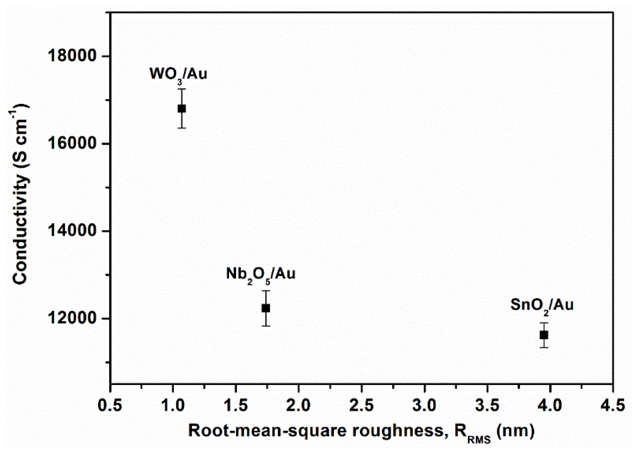
The roughness of the dielectric layers affects the optical properties of the DMD coatings. When the dielectric films were coated with 10 nm of Au, the topography was replicated to the Au films. The RRMS values of this bilayer (SnO2/Au) were more than double that of Nb2O5/Au and almost four times higher than that of WO3/Au. As the optical properties are related to both the roughness and conductivity, the conductivity of Au deposited on top of the dielectrics was also measured. Figure 3 presents the conductivity as a function of roughness of the three dielectrics coated with 10 nm thick Au films. The coating presenting the highest conductivity value was Au deposited on WO3, followed by Nb2O5/Au and SnO2/Au. It was also observed that the smoother the surface, the more conductive the coating. The relationship between roughness, conductivity and optical properties of thin films is also explained by the Fund–Sondheimer and Mayadas–Shatzkes scattering models [31,32,33]; the smoother and more conductive they are, the higher the reflectance in the infrared range.
Due to the relatively high roughness of the SnO2 film, the SnO2/Au/SnO2 coating system required a thicker Au film to achieve a comparable RIR to those of WO3/Au/WO3 and Nb2O5/Au/Nb2O5. However, increasing the Au thickness resulted in a trade-off with the Tvis, as can be observed in SnO2 (40 nm)/Au (40 nm)/SnO2 (40 nm) in Table 4, with 71% RIR, but 53% Tvis.
Other factors that might be contribute to the electrical and optical properties of low-e coatings have been discussed in other studies [3,34]. Other than the surface roughness, the residual gases present during sputtering [34], the percolation threshold of the metallic layer [3,35] and the sputtering deposition parameters might play a role.
In conclusion, the optimum thickness values for Au, as determined by Փ, are 15, 40 and 20 nm for WO3, SnO2 and Nb2O5, respectively.

3.1.2. Dielectric Layer

The optimisation of the thickness of the dielectric layer in a DMD system is critical to achieve low emissivity and high transmittance in the visible range [36]. DMD coating systems with different dielectric thickness combined with 15 nm of Au in the case of WO3, 40 nm of Au for SnO2 and 20 nm of Au for Nb2O5 were prepared. The key performance parameters, such as the Tvis, RIR and Փ, were then measured and are presented in Table 3. The WO3/Au/WO3 system exhibited the highest Figure of Merit (Φ = 0.40) when the WO3 was 40 nm. For the SnO2/Au/SnO2 system, the optimal performance was achieved with 50–60 nm SnO2 layer, yielding to Φ = 0.39. And the Nb2O5/Au/Nb2O5 system, achieved the highest Figure of Merit (Φ = 0.43) of all systems with 40–50 nm Nb2O5 layer, making it the best-performing configuration in terms of optical properties.
The Transmittance (T) and Reflectance (R) spectra of each of the three coating systems with optimised thickness are plotted in Figure 4a, and the conductivity vs. the emissivity is presented in Figure 4b. The highest Tvis value was demonstrated by WO3/Au/WO3 with 63%, followed by the system with SnO2 (57%) and the system with Nb2O5 (56%). The highest RIR (76%) was exhibited by the coating system with Nb2O5 as the dielectric, followed by SnO2 and WO3, with 68% and 63%, respectively. The visible transmittance of the multilayer coatings, while lower than that of some commercial low-emissivity coatings (>70%), still remain suitable for applications requiring moderate light transmission and solar control. Previous studies, such as Boyce et al. [37], indicate that glazing with a transmittance range of 25–38% still allows approximately 85% of subjects to be clearly seen, suggesting that the current Tvis provides adequate visibility for architectural or automotive applications. Further improvements in optical performance could be achieved in future work through strategies such as antireflective designs or optimization of multilayer dielectric structures.
The infrared optical properties of materials are dictated by the combination of factors from the electronic structure to the thermal emission characteristics. IR reflectance values are related to the conductivity and emissivity by the Hagen Ruben Equation, where emissivity, ε, is defined as the ratio of thermal radiation emitted by a surface to the thermal radiation emitted by a blackbody [4]. This link is explained by the Drude theory [38], where electron clouds in a metal shield the electromagnetic field (such as the incident light) by reflecting it. Hence, the higher the conductivity, the higher the IR reflectance and the lower the emissivity. This can be observed in Figure 4b, where the highest conductivity and lowest emissivity also resulted in the highest infrared reflectance (RIR) which is the case of the Nb2O5/Au/Nb2O5 coating system with a conductivity of 2.8 × 10⁴ S cm−1 and emissivity of 0.04.
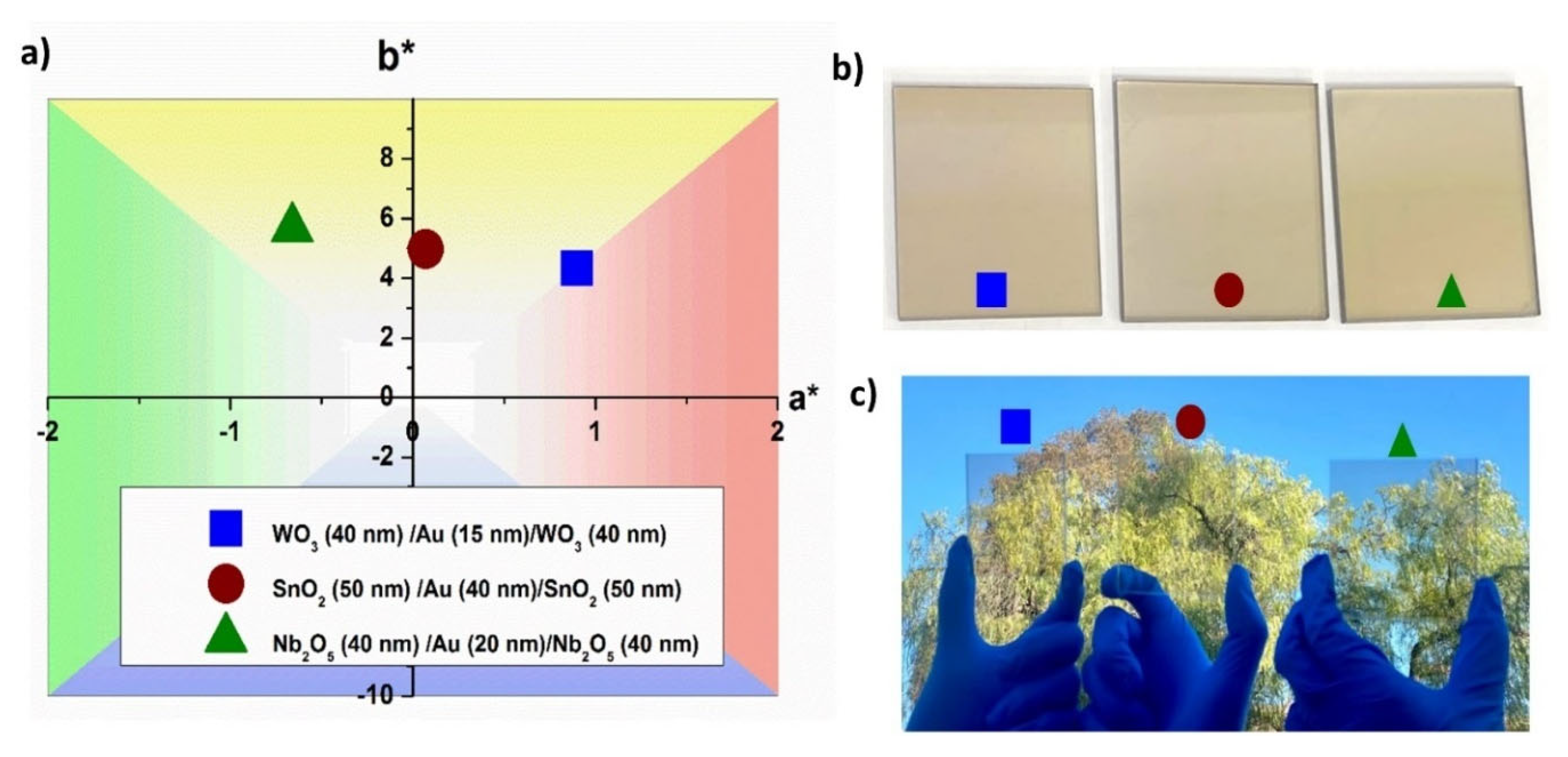
Equally important to the optical performance parameters, such as the TVIS, RIR and ε, is the colour of the coating, especially in consumer applications. The colour of the coating systems was measured and plotted in the CIE L*a*b* D65/10 colour space. As presented in Figure 5a, the SnO2/Au/SnO2 coating system displayed a pale yellow colour, which was also the most neutral (a* and b* close to 0). Figure 5 also presents a photograph of the coating systems against a white background (Figure 5b) and in outdoor conditions (Figure 5c). Even though the Au-based coating systems display a golden/yellow colour, especially against a white background, all coating variations demonstrated a neutral and transparent colour in outdoor conditions, which makes the coating barely visible to the human eye.

3.2. Environmental Durability

Optical properties are not the only factor to be considered when designing low-e coatings for real-world applications. Coatings should also be environmentally durable and able to withstand humid and corrosive conditions during their service lifetime (at least 20 years) [39].
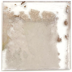
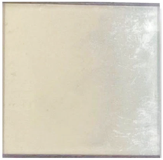
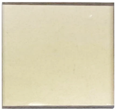
To evaluate the resistance of the coatings against corrosion, three different DMD systems were tested in a salt spray chamber under the conditions defined in ASTM B117-18. The visual and optical changes of the samples were first inspected after 24 h and are presented in Table 4. After just 24 h, the only DMD system without any visual or optical changes was Nb2O5/Au/Nb2O5. SnO2/Au/SnO2 displayed a minor optical change with only 2% decrease in the RIR and no change in Tvis. However, this coating started fading at the edge of the sample. WO3/Au/WO3 demonstrated significant deterioration with a reduction of 12% and 54% for Tvis and RIR, respectively, due to the coating dissolution as a result of severe corrosion. This could be attributed to the adhesion issues between WO3 and PC also reported by Vernardou et al. [40].
Table 4. Photographs and optical parameters of Au-based low-e coatings after 24 h in the salt spray corrosion chamber.
WO3/Au/WO3SnO2/Au/SnO2Nb2O5/Au/Nb2O5
Coatings 15 01231 i001Coatings 15 01231 i002Coatings 15 01231 i003
ΔTvis = −12%, ΔRIR = −54%ΔTvis = 0%, ΔRIR = −2%ΔTVvis= 0%, ΔRIR = 0%
The superiority of Nb2O5 in protecting the Au might be related to a denser film in comparison to SnO2 and WO3. It is well established for DC magnetron sputtering that increasing the target power (and thus the energy flux to the substrate) enhances adatom mobility and ion bombardment during growth, producing films with lower porosity, smoother surfaces and a denser microstructure, which can in turn improve barrier performance [41,42,43].
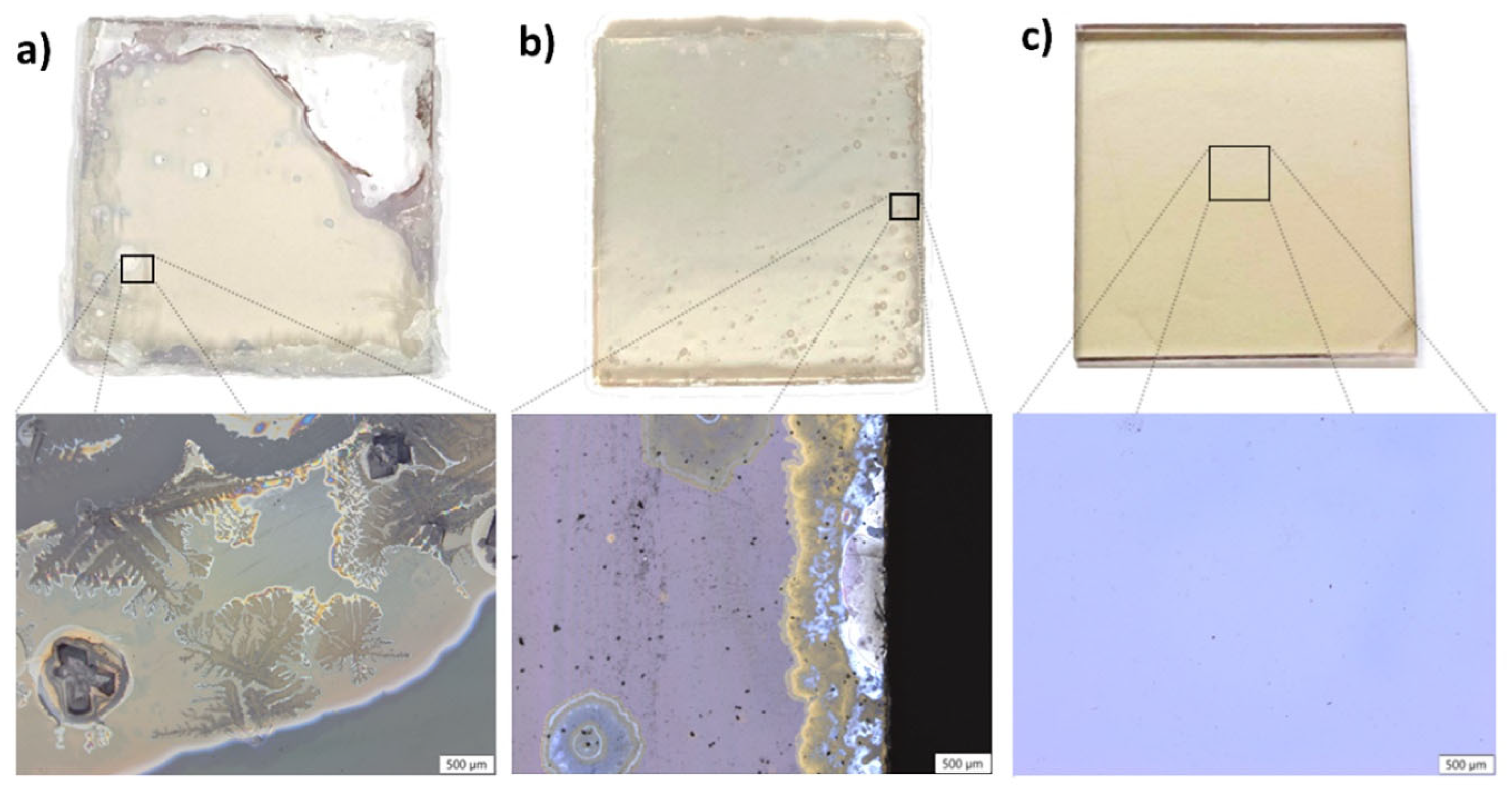
As previously reported by Llusca et al. [44], 10 nm of sputtered SiO2 adhesion layer with 5 µm of a transparent HC resin improved the corrosion and abrasion resistance of Ag-based low-e coatings. Therefore, the SiO2/HC system was applied on top of the WO3 (40 nm)/Au (15 nm)/WO3 (40 nm), SnO2 (50 nm)/Au (40 nm)/SnO2 (50 nm) and Nb2O5 (40 nm)/Au (20 nm)/Nb2O5 (40 nm) coating systems. All three coating systems achieved an adhesion rating of 5B and showed no optical changes after the application of the SiO2/HC protective layers. The samples were subsequently tested in the salt spray corrosion chamber. As shown in Figure 6, with the additional SiO2/HC, WO3/Au/WO3 extended its lifetime from 24 h to 48 h; however, after 48 h, the coating delaminated (Figure 6a). This can be again linked to the lack of WO3 adhesion to the PC substrate and the low corrosion resistance of WO3 towards NaCl. Micro-pitting corrosion was observed and grew larger with the salt spray exposure and remarkably degraded the optical properties of the sample with −15% in Tvis and −40% in RIR.
More importantly, the additional SiO2/HC protective coating on top of SnO2/Au/SnO2 improved the longevity of the coating system up to 1000 h (minimum test duration required for exterior automotive components). The tested coating system showed no optical changes and demonstrated a superior corrosion resistance to previously reported Ag- and Ag-Cu-based low-e coatings on PC substrates [17]. However, the improved coating system started to exhibit white casts on the edges (see Figure 6b) due to the corrosive medium penetrating from the unsealed edges or through pin-hole defects in the coating. Based on previous studies [16,17,45], the corrosion of similar coatings also initiated from white casts that grew larger and ended up forming cracks and wrinkles.
Nb2O5/Au/Nb2O5 demonstrated no optical or visual changes in the salt spray chamber up to 1000 h without SiO2/HC, suggesting that the hard-coat protection was not necessary in this case. Nevertheless, the hard-coat protection provided abrasion resistance to the multilayer coating system. Table 5 presents the results of the Steel Wool and Bayer abrasion resistance tests of the Nb2O5/Au/Nb2O5 coating system with and without the SiO2/HC protective layer. As shown in the table, a slight improvement was observed by adding a SiO2/HC protective layer, which reduced the ΔH% from 5.2% to 1.5% for the Steel Wool test and from 9.8% to 5.9% for the Bayer test. Although these quantitative improvements were evident from the haze measurements, no visible differences were observed between the samples with or without the SiO2/hard coat after either the Steel Wool or Bayer abrasion tests.
The corrosion and abrasion resistance results suggest that the Nb2O5/Au/Nb2O5/SiO2/HC low-e coating system could be used as a first surface coating, without the need to isolate them from the environment. The fact that these have been optimised for plastic substrates opens up the possibility of applying them in flexible films via roll-to-roll processes. However, to fully affirm that these coatings could be employed for commercial use, further testing and validation should be performed. In addition, for large-scale production, spray-coating may be more suitable than dip-coating, as it can produce more uniform coatings over larger areas and has been reported to achieve higher adhesion strength [46].

4. Conclusions

Au-based low-e coating systems were grown on PC substrates using magnetron sputtering. Thin Au films were sandwiched between WO3, SnO2 and Nb2O5 in DMD structures and investigated and optimised thoroughly by varying the thickness of both the metallic and dielectrics layers. The best combination of materials determined by high IR reflectance and high visible transmittance was found to be for the Nb2O5 (40 nm)/Au (20 nm)/Nb2O5 (40 nm), which resulted in 56% Tvis and 76% RIR. This coating system also proved to be the most corrosion-resistant, as it survived as long as 1000 h in the salt spray test (minimum test duration required for automotive components) without observed changes. An additional SiO2 (10 nm)/hard-coat (5 µm) protective coating was then applied to further enhance the abrasion resistance without affecting the optical properties. The simplicity and robustness of the presented coating design suggest this to be a promising alternative to Ag-based low-e coatings. In addition, the fact that these have been optimised for plastic substrates opens up the possibility of applying them in flexible films via roll-to-roll processes.

Author Contributions

Conceptualization, M.L.J.; Methodology, W.N.S.W.S.; Validation, K.Z., P.J.M. and M.L.J.; Investigation, W.N.S.W.S.; Resources, P.J.M.; Data curation, W.N.S.W.S.; Writing—original draft, W.N.S.W.S.; Writing—review & editing, K.Z. and M.L.J.; Supervision, K.Z., P.J.M. and M.L.J.; Project administration, P.J.M.; Funding acquisition, P.J.M. All authors have read and agreed to the published version of the manuscript.

Funding

This research was funded by the Malaysian Automotive, Robotics and IoT Institute (MARii).

Institutional Review Board Statement

Not applicable.

Informed Consent Statement

Not applicable.

Data Availability Statement

Data is contained within the article.

Conflicts of Interest

The authors have no competing interests to declare that are relevant to the content of this article.

References

  1. Amirkhani, S.; Bahadori-Jahromi, A.; Mylona, A.; Godfrey, P.; Cook, D. Impact of low-e window films on energy consumption and CO2 emissions of an existing UK hotel building. Sustainability 2019, 11, 4265. [Google Scholar] [CrossRef]
  2. Ding, G.; Clavero, C. Silver-Based Low-Emissivity Coating Technology for Energy-Saving Window Applications. In Modern Technologies for Creating the Thin-Film Systems and Coatings; IntechOpen: Rijeka, Croatia, 2017. [Google Scholar]
  3. Dalapati, G.K.; Kushwaha, A.K.; Sharma, M.; Suresh, V.; Shannigrahi, S.; Zhuk, S.; Masudy-Panah, S. Transparent heat regulating (THR) materials and coatings for energy saving window applications: Impact of materials design, micro-structural, and interface quality on the THR performance. Prog. Mater. Sci. 2018, 95, 42–131. [Google Scholar] [CrossRef]
  4. Dalapati, G.K.; Masudy-Panah, S.; Chua, S.T.; Sharma, M.; Wong, T.I.; Tan, H.R.; Chi, D. Color tunable low cost transparent heat reflector using copper and titanium oxide for energy saving application. Sci. Rep. 2016, 6, 20182. [Google Scholar] [CrossRef]
  5. Jelle, B.P.; Kalnæs, S.E.; Gao, T. Low-emissivity materials for building applications: A state-of-the-art review and future research perspectives. Energy Build. 2015, 96, 329–356. [Google Scholar] [CrossRef]
  6. Sahu, D.R.; Huang, J.L. Design of ZnO/Ag/ZnO multilayer transparent conductive films. Mater. Sci. Eng. B 2006, 130, 295–299. [Google Scholar] [CrossRef]
  7. Sahu, D.R.; Huang, J.-L. High quality transparent conductive ZnO/Ag/ZnO multilayer films deposited at room temperature. Thin Solid Film. 2006, 515, 876–879. [Google Scholar] [CrossRef]
  8. Neghabi, M.; Behjat, A.; Ghorashi, S.; Salehi, S. The effect of annealing on structural, electrical and optical properties of nanostructured ZnS/Ag/ZnS films. Thin Solid Film. 2011, 519, 5662–5666. [Google Scholar] [CrossRef]
  9. Wu, H.-W.; Yang, R.-Y.; Hsiung, C.-M.; Chu, C.-H. Influence of Ag thickness of aluminum-doped ZnO/Ag/aluminum-doped ZnO thin films. Thin Solid Film. 2012, 520, 7147–7152. [Google Scholar] [CrossRef]
  10. Ding, G.; Clavero, C.; Schweigert, D.; Le, M. Thickness and microstructure effects in the optical and electrical properties of silver thin films. AIP Adv. 2015, 5, 117234. [Google Scholar] [CrossRef]
  11. Zhao, Z.; Alford, T.L. The optimal TiO2/Ag/TiO2 electrode for organic solar cell application with high device-specific Haacke figure of merit. Sol. Energy Mater. Sol. Cells 2016, 157, 599–603. [Google Scholar] [CrossRef]
  12. Sharma, V.; Kumar, P.; Kumar, A.; Asokan, K.; Sachdev, K. High-performance radiation stable ZnO/Ag/ZnO multilayer transparent conductive electrode. Sol. Energy Mater. Sol. Cells 2017, 169, 122–131. [Google Scholar] [CrossRef]
  13. Nur-E-Alam, M.; Vasiliev, M.; Alameh, K. Dielectric/metal/dielectric (DMD) multilayers: Growth and stability of ultra-thin metal layers for transparent heat regulation (THR). In Energy Saving Coating Materials; Elsevier: Amsterdam, The Netherlands, 2020; pp. 83–112. [Google Scholar]
  14. Kim, S.; Lee, J.L. Design of dielectric/metal/dielectric transparent electrodes for flexible electronics. J. Photonics Energy 2012, 2, 021215. [Google Scholar] [CrossRef]
  15. Ross, R. Observations on humidity-induced degradation of Ag-based low-emissivity films. Sol. Energy Mater. 1990, 21, 25–42. [Google Scholar] [CrossRef]
  16. Ando, E.; Miyazaki, M. Moisture degradation mechanism of silver-based low-emissivity coatings. Thin Solid Film. 1999, 351, 308–312. [Google Scholar] [CrossRef]
  17. Shamsuddin, W.N.S.W.; Roccisano, A.; Zuber, K.; Murphy, P.J.; Jane, M.L. Environmentally robust Ag–Cu based low-e coatings. Sol. Energy Mater. Sol. Cells 2022, 248, 112033. [Google Scholar] [CrossRef]
  18. Al-Kuhaili, M.F. Enhancement of plasmonic transmittance of porous gold thin films via gold/metal oxide bi-layers for solar energy-saving applications. Sol. Energy 2019, 181, 456–463. [Google Scholar] [CrossRef]
  19. Bennett, J.M.; Ashley, E. Infrared reflectance and emittance of silver and gold evaporated in ultrahigh vacuum. Appl. Opt. 1965, 4, 221–224. [Google Scholar] [CrossRef]
  20. Holland, L.; Siddall, G. Heat-reflecting windows using gold and bismuth oxide films. Br. J. Appl. Phys. 1958, 9, 359. [Google Scholar] [CrossRef]
  21. Al-Kuhaili, M.; Al-Aswad, A.; Durrani, S.; Bakhtiari, I. Energy-saving transparent heat mirrors based on tungsten oxide–gold WO3/Au/WO3 multilayer structures. Sol. Energy 2012, 86, 3183–3189. [Google Scholar] [CrossRef]
  22. Andersson, K.E.; Veszelei, M.; Roos, A. Zirconium nitride based transparent heat mirror coatings—Preparation and characterisation. Sol. Energy Mater. Sol. Cells 1994, 32, 199–212. [Google Scholar] [CrossRef]
  23. Shamsuddin, W.N.S.W.; Zuber, K.; Murphy, P.J.; Jane, M.L. Environmental durability of soft low-e coatings: A review. Sol. Energy Mater. Sol. Cells 2024, 266, 112673. [Google Scholar] [CrossRef]
  24. Patil, A.; Patel, A.; Purohit, R. An overview of Polymeric Materials for Automotive Applications. Mater. Today Proc. 2017, 4, 3807–3815. [Google Scholar] [CrossRef]
  25. Solovyev, A.; Rabotkin, S.; Kovsharov, N. Polymer films with multilayer low-E coatings. Mater. Sci. Semicond. Process. 2015, 38, 373–380. [Google Scholar] [CrossRef]
  26. Pracchia, J.A.; Simon, J.M. Transparent heat mirrors: Influence of the materials on the optical characteristics. Appl. Opt. 1981, 20, 251–258. [Google Scholar] [CrossRef] [PubMed]
  27. Leftheriotis, G.; Yianoulis, P.; Patrikios, D. Deposition and optical properties of optimised ZnS/Ag/ZnS thin films for energy saving applications. Thin Solid Film. 1997, 306, 92–99. [Google Scholar] [CrossRef]
  28. Abdullah, N.; Ismail, N.; Nuruzzaman, D. Preparation of tin oxide (SnO2) thin films using thermal oxidation. IOP Conf. Ser. Mater. Sci. Eng. 2018, 319, 012022. [Google Scholar] [CrossRef]
  29. Gnanam, S.; Rajendran, V. Luminescence properties of EG-assisted SnO2 nanoparticles by sol-gel process. Dig. J. Nanomater. Biostruct. 2010, 5, 699–704. [Google Scholar]
  30. Li, Y.; Xin, Q.; Du, L.; Qu, Y.; Li, H.; Kong, X.; Wang, Q.; Song, A. Extremely Sensitive Dependence of SnOx Film Properties on Sputtering Power. Sci. Rep. 2016, 6, 36183. [Google Scholar] [CrossRef] [PubMed]
  31. Wissmann, P.; Finzel, H.-U. Electrical Resistivity of Thin Metal Films; Springer Science & Business Media: Berlin/Heidelberg, Germany, 2007; Volume 223. [Google Scholar]
  32. James, R.A.; Stapleton, A.J.; Hughes, A.; Charrault, E.; Zuber, K.; Switalska, E.; Evans, D.; Murphy, P.; Llusca, M. Metallic Adhesive Layers for Ag-Based First Surface Mirrors. Adv. Eng. Mater. 2018, 20, 1800106. [Google Scholar] [CrossRef]
  33. Zhou, T.; Zheng, P.; Pandey, S.C.; Sundararaman, R.; Gall, D. The electrical resistivity of rough thin films: A model based on electron reflection at discrete step edges. J. Appl. Phys. 2018, 123, 155107. [Google Scholar] [CrossRef]
  34. Nakanishi, Y.; Kato, K.; Omoto, H.; Tomioka, T. Improvement in salt-water durability of Ag thin films deposited by magnetron sputtering using argon and nitrogen mixed gas. Vacuum 2013, 87, 232–236. [Google Scholar] [CrossRef]
  35. Lansåker, P.; Backholm, J.; Niklasson, G.; Granqvist, C. TiO2/Au/TiO2 multilayer thin films: Novel metal-based transparent conductors for electrochromic devices. Thin Solid Film. 2009, 518, 1225–1229. [Google Scholar] [CrossRef]
  36. Köstlin, H.; Frank, G. Optimization of transparent heat mirrors based on a thin silver film between antireflection films. Thin Solid Film. 1982, 89, 287–293. [Google Scholar] [CrossRef]
  37. Boyce, P.; Eklund, N.; Mangum, S.; Saalfield, C.; Tang, L. Minimum acceptable transmittance of glazing. Int. J. Light. Res. Technol. 1995, 27, 145–152. [Google Scholar] [CrossRef]
  38. Dresselhaus, M.; Dresselhaus, G.; Cronin, S.B.; Filho, A.G.S. Drude theory–free carrier contribution to the optical properties. In Solid State Properties: From Bulk to Nano; Springer: Berlin/Heidelberg, Germany, 2018; pp. 329–344. [Google Scholar]
  39. Hu, C.; Liu, J.; Wang, J.; Gu, Z.; Li, C.; Li, Q.; Li, Y.; Zhang, S.; Bi, C.; Fan, X.; et al. New design for highly durable infrared-reflective coatings. Light Sci. Appl. 2018, 7, 17175. [Google Scholar] [CrossRef] [PubMed]
  40. Vernardou, D.; Drosos, H.; Spanakis, E.; Koudoumas, E.; Katsarakis, N.; Pemble, M. Electrochemical properties of amorphous WO3 coatings grown on polycarbonate by aerosol-assisted CVD. Electrochim. Acta 2012, 65, 185–189. [Google Scholar] [CrossRef]
  41. Salunkhe, P.; AV, M.A.; Kekuda, D. Structural, spectroscopic and electrical properties of dc magnetron sputtered NiO thin films and an insight into different defect states. Appl. Phys. A 2021, 127, 390. [Google Scholar] [CrossRef]
  42. Konstantinidis, S.; Dauchot, J.; Hecq, M. Titanium oxide thin films deposited by high-power impulse magnetron sputtering. Thin Solid Film. 2006, 515, 1182–1186. [Google Scholar] [CrossRef]
  43. Koski, K.; Hölsä, J.; Juliet, P. Properties of aluminium oxide thin films deposited by reactive magnetron sputtering. Thin Solid Film. 1999, 339, 240–248. [Google Scholar] [CrossRef]
  44. Jane, M.L.; Hall, C.; Pająk, A.; Patil, A.; Switalska, E.; Yunos, L.N.; Reeks, L.B.; Zuber, K. Coated Articles with A Low-E Coating and/or A Hard Coat. Australian Provisional Patent Application AU2022901475A0, 31 May 2022. [Google Scholar]
  45. Koike, K.; Shimada, K.; Fukuda, S. Aggregation in thin-film silver: Induced by chlorine and inhibited by alloying with two dopants. Corros. Sci. 2009, 51, 2557–2564. [Google Scholar] [CrossRef]
  46. Yang, H.; Dong, Y.; Li, X.; Gao, Y.; He, W.; Liu, Y.; Mu, X.; Zhao, Y.; Fu, W.; Wang, X.; et al. Development of a mechanically robust superhydrophobic anti-corrosion coating using micro-hBN/nano-Al2O3 with multifunctional properties. Ceram. Int. 2025, 51, 491–505. [Google Scholar] [CrossRef]
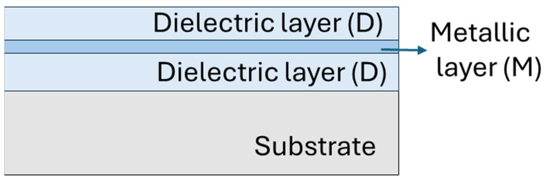
Figure 1. A typical basic low-e coating design: dielectric/metal/dielectric (DMD).
Coatings 15 01231 g001
Figure 2. Three-dimensional AFM 1.6 × 1.6 µm topographic images and RRMS values of 40 nm thick dielectric layers sputtered on glass, with and without 10 nm of Au on top: (a) WO3; (b) WO3/Au; (c) SnO2; (d) SnO2/Au; (e) Nb2O5; (f) Nb2O5/Au on glass substrates. Different colour scales are used in all images to highlight the peak-to-valley height of each film.
Coatings 15 01231 g002
Figure 3. Conductivity vs. surface roughness of 40 nm thick dielectric films coated with 10 nm of Au.
Coatings 15 01231 g003
Figure 4. WO3 (40 nm)/Au (15 nm)/WO3 (40 nm), SnO2 (50 nm)/Au (40 nm)/SnO2 (50 nm) and Nb2O5 (40 nm)/Au (20 nm)/Nb2O5 (40 nm) coatings on polycarbonate substrates: (a) Transmittance (T) and Reflectance (R) spectra and (b) conductivity vs. emissivity.
Coatings 15 01231 g004
Figure 5. Colour evaluation of the prototypes of Au-based coatings on polycarbonate substrate: (a) CIE L*a*b* D65/10 colour values and (b) photographs of the prototypes against a white background, and (c) outdoor condition.
Coatings 15 01231 g005
Figure 6. Photographs and microscope images of Au-based multilayer coatings after salt spray exposure: (a) WO3/Au/WO3/SiO2/HC after 48 h; (b) SnO2/Au/SnO2/SiO2/HC after 1000 h; (c) Nb2O5/Au/Nb2O5 after 1000 h. The scale bars of all microscope images represent 500 µm in length.
Coatings 15 01231 g006
Table 1. Sputtering deposition parameters for Au, WO3, SnO2, Nb2O5 and SiO2.
MaterialPower (W)Ar (sccm)O2 (sccm)Working Pressure (mbar)Deposition Rate (nm/min)
Au3001503.0 × 10−37.32
WO320015506.5 × 10−30.84
SnO25015234.0 × 10−30.72
Nb2O5150050703.3 × 10−34.67
SiO22000230453.3 × 10−36.67
Table 2. Visible transmittance (Tvis), infrared reflectance (RIR) and Figure of Merit (Փ) of different thickness values of Au combined with 40 nm thick dielectric films in DMD designs on polycarbonate substrates. Thickness values are reported with the standard deviations based on the average of six measurements. Highlighted in green are the best-performing samples for each configuration.
Thickness of Au Layers (nm)Standard Deviation (nm)Tvis (%)RIR (%)Փ
WO3(40 nm)/Au/WO3 (40 nm)
101.2673350.26
150.7563630.40
170.8257700.40
SnO2 (40 nm)/Au/SnO2 (40 nm)
100.8969150.10
201.0367400.27
301.0462510.32
401.3253710.38
451.4129870.25
Nb2O5 (40 nm)/Au/Nb2O5 (40 nm)
101.1770210.15
151.0566630.42
200.7556760.43
251.0348830.40
Table 3. Visible transmittance (Tvis), infrared reflectance (RIR) and Figure of Merit (Փ) of various dielectric thicknesses combined with 15 nm of Au for WO3, 40 nm of Au for SnO2 and 20 nm of Au for Nb2O5 DMD coatings. Thickness values are reported with the standard deviations based on the average of six measurements. Highlighted in green are the best-performing samples for each configuration.
Thickness of Dielectric Layer (nm)Standard Deviation (nm)Tvis(%)RIR(%)Փ
WO3/Au (15 nm)/WO3
301.4754690.37
350.8257690.39
401.0363630.40
451.1763620.39
SnO2/Au (40 nm)/SnO2
402.0753710.38
501.7257680.39
600.7559660.39
Nb2O5/Au (20 nm)/Nb2O5
351.4751790.40
401.0356760.43
500.7560720.43
601.3760660.40
Table 5. Changes in haze (ΔH%) of Nb2O5/Au/Nb2O5 with and without SiO2/HC topcoat after Steel Wool and Bayer abrasion tests.
Δ H%
Multilayer SamplesSteel WoolBayer
Nb2O5/Au/Nb2O55.29.8
Nb2O5/Au/Nb2O5/SiO2/HC1.55.9
Commercial abrasion-resistant polycarbonate (Makrolon AR)0.93.0
Disclaimer/Publisher’s Note: The statements, opinions and data contained in all publications are solely those of the individual author(s) and contributor(s) and not of MDPI and/or the editor(s). MDPI and/or the editor(s) disclaim responsibility for any injury to people or property resulting from any ideas, methods, instructions or products referred to in the content.