Article

Controlled Nanopore Fabrication on Silicon via Surface Plasmon Polariton-Induced Laser Irradiation of Metal–Insulator–Metal Structured Films

by
Sifan Huo
1,2,
Sipeng Luo
3,
Ruishen Wang
4,
Jingnan Zhao
1,2,*,
Wenfeng Miao
1,
Zhiquan Guo
1,2 and
Yuanchen Cui
5
1
School of Mechanical Engineering, Tianjin University of Science and Technology, Tianjin 300000, China
2
Tianjin Key Laboratory of Integrated Design and On-Line Monitoring for Light Industry & Food Machinery and Equipment, Tianjin 300000, China
3
Shenyang SIASUN Robot & Automation Co., Ltd., No. 16, Jinhui Street, Hunnan New District, Shenyang 110000, China
4
School of Mechanical and Energy Engineering, Beijing University of Technology, Beijing 100124, China
5
Anton Paar USA, 10215 Timber Ridge Dr, Ashland, VA 23005, USA
*
Author to whom correspondence should be addressed.
Coatings 2025, 15(10), 1187; https://doi.org/10.3390/coatings15101187
Submission received: 6 September 2025 / Revised: 5 October 2025 / Accepted: 6 October 2025 / Published: 10 October 2025
(This article belongs to the Section Surface Characterization, Deposition and Modification)

Abstract

In this study, we present a cost-effective approach for fabricating nanopores on single-crystal silicon using a silver–alumina–silver (Ag/AAO/Ag) metal–insulator–metal (MIM) structured mask. Self-ordered porous anodic aluminum oxide (AAO) films were prepared via two-step anodization and coated with silver layers on both sides to form the MIM structure. When irradiated with a 532 nm nanosecond laser, the MIM mask excites surface plasmon polaritons (SPPs), resulting in a localized field enhancement that enables the etching of nanopores into the silicon substrate. This method successfully produced nanopores with diameters as small as 50 nm and depths up to 28 nm. The laser-induced SPP-assisted machining significantly enhances the specific surface area of the processed surface, making it promising for applications in catalysis, biosensing, and microcantilever-based devices. For instance, an increased surface area can improve catalytic efficiency by providing more active sites, and enhance sensor sensitivity by amplifying response signals. Compared to conventional lithographic or focused ion beam techniques, this method offers simplicity, low cost, and scalability. The proposed technique demonstrates a practical and efficient route for the large-area subwavelength nanostructuring of silicon surfaces.

1. Introduction

Micro-nanofabrication is a machining technology that involves the creation of micropores, microgrooves, and complex microfabricated surfaces on tiny or thin workpieces. Nanopores, as a type of microporous structure, have nanoscale dimensions (typically between 1 and 100 nanometers in diameter) and can exist in a variety of materials, including metals, ceramics, polymers, and biomolecules. In recent years, solid-state nanopores have attracted extensive attention and research in the fields of nanotechnology, materials science, biosensing, and optical devices [1,2,3]. Compared with soft materials, solid-state materials have the advantages of high stability and rigidity [4] and can be used as molecular sensors to detect the presence and concentration of specific molecules by monitoring the transport of molecules through the pores. When the target molecule is driven by an electric field through the nanopore, it will instantaneously modulate the ionic current passing through the pore, generating a characteristic current blockage pulse signal. By analyzing the amplitude, duration, and frequency of these pulses, the detection and identification of single molecules can be achieved. By introducing a porous structure on the surface of a microcantilever beam biosensor and constructing a receptor layer using a physical adsorption method [5], the researchers succeeded in increasing the frequency shift signal up to 75 times the original signal, which resulted in a significant improvement in the detection response [6]. Solid-state nanopores can also be used as nanoscale templates for the preparation of various nanomaterials such as nanoparticles, nanowires, and nanosheets. This highly controllable method allows for the preparation of nanomaterials with specific structures and properties. These nanomaterials have a wide range of applications in energy storage, catalysis, optoelectronics, and biomedicine.
The commonly used methods for the fabrication of solid-state nanoholes are focused ion beam (FIB), focused electron beam (FEB), and inductively coupled plasma (ICP) [7,8,9,10]. With the development of plasma technology, the nanopore preparation process based on surface plasma lithography has become one of the new available methods [11]. Surface plasmons (SPs) are resonant electromagnetic waves that exist at the interface between a medium and a metal demarcation and propagate along the metal surface [12,13]. This is due to the interaction between the photons of incident light and the free electrons on the metal surface, creating an excited state on the demarcation surface. When the frequency of the incident photons is the same as the frequency of the free electrons, this interaction resonates to form a resonant wave. Such resonant waves are often called SPPs [14]. Researchers have discovered that they can use the excitation of surface plasmas to break through the diffraction limit of conventional optical lithography to achieve micro- and nanoscale processing. Surface plasmon technology is widely used in nanophotonics [15], plasma sensors [16], biosensors [17,18], hypersurfaces [19], and interferometric lithography with surface plasmons [20]. It has been demonstrated that SPPs help to amplify the evanescent wave and realize super-resolution imaging lithography [21,22,23].
Realizing the excitation of the surface plasmas requires making the incident light wave vector match the surface plasma wave vector [14]. Therefore, we need to utilize some special structures, and there are two generally used excitation pathways: prism coupling [24] and grating coupling [25]. The typical structures for prism coupling are Kretschaman [24] and Otto [26], two prism coupling methods which utilize the generated swift wave to reach the matching condition of the wave vector to excite the surface plasmas. Grating coupling [25] refers to the utilization of a periodic grating structure to form surface plasmas in the direction perpendicular to the grating structure when the transverse wave vector of the diffraction effect matches the wave vector of the SPPs. Adjusting the parameter information, such as the wavelength, angle, grating period, or diffraction level of the incident light, will make it meet the excitation conditions of the SPPs. All of them can realize the regulation control of the surface plasmas to a certain extent. Compared with prism coupling, grating coupling is more tunable. The grating structure can realize the optical coupling of different wavelengths by adjusting the grating period, so it has a stronger tuning performance and higher coupling efficiency. Grating coupling is more controllable, and the light field distribution can be precisely controlled by adjusting the structural parameters of the grating. And its structure is also more compact [27].
AAO has a highly ordered arrangement of pores and has attracted a broad interest for its unique nanocyclic pore structure. Its anodic oxidation of aluminum flakes in an acidic electrolyte solution results in the formation of porous anodic oxide films with a large number of nanoscale pores [28]. It is extremely easy to obtain AAO with an ideal arrangement of grating structures and a high aspect ratio [29]. The surface pores of the AAO film are relatively uniformly arranged, orderly, and period adjustable, which can be used as a simple grating structure to excite surface plasmas. The hole size, arrangement distribution, and symmetry of the AAO film itself correspond to the period of the grating. Currently, most research on electromagnetic waves associated with surface plasmon polaritons (SPPs) is based on the visible light spectrum, specifically within the wavelength range of 400–750 nm. Compared to other metals, metallic silver exhibits lower optical loss and stronger surface plasmon resonance effects. In this paper, we propose a composite structure of Ag/AAO/Ag to realize the excitation of SPPs and the preparation of nanoporous surfaces using the excited SPPs, based on the Au/AAO/Au structure prepared by Miao et al. [30]. Compared with metallic gold as the excitation material, metallic silver possesses better electrical conductivity as well as minimal absorption loss, which can more easily realize the excited surface plasmas. The fabrication of porous patterns on silicon using an AAO film can also utilize the AAO film as a hard mask. Gold or other precious metals can be deposited on the AAO film, and then etched using hydrofluoric acid and hydrogen peroxide. The precious metal layer reduces the surface energy, promoting the oxidation and dissolution of silicon, and ultimately forming ordered nanostructures through the pores of the AAO film [31]. Although this method is simpler than surface plasmon excitation, it is overly dependent on the quality and manufacturing accuracy of the AAO template and is less flexible than plasmon excitation.
In this paper, an MIM structure based on a combination of a nanometer-thick silver layer and AAO film is proposed for the excitation of surface plasmas. By controlling the laser energy density and irradiating the MIM film to excite the surface plasmas, the nanoholes can be simply and efficiently processed on the single-crystal silicon surface. The fabrication process provides a new idea and method for using porous anodized aluminum oxide films and preparing nanoholes at a very low cost compared to the existing processing methods, and it is reproducible. This paper aims to explore and realize the fabrication method of nanopores based on surface plasmas, which provides new ideas and directions for research and application in the field of micro- and nanofabrication.

2. Theoretical Analysis

2.1. Theoretical Calculations Related to Surface Plasmas

Surface plasmon polaritons are regions where the surface of a medium is in contact with plasmas, and the surface plasma can be excited when an energetic particle (such as a laser beam) interacts with the surface of the medium. The whole process satisfies the set of Maxwell’s equations and their fluctuation equations, which are dispersion relations of the relevant theory [32].
SPPs are collective excitations generated by the interaction of photons with electrons on the metal surface. When light strikes the metal surface, the photon energy is transferred to the metal’s free electrons, and the surface plasma wave is excited. This surface wave propagates on the metal surface and has fluctuating properties similar to photons [23]. Continuing the derivation based on the above fundamental equations, two constraints on the excitation of SPs can be derived: the real parts of the dielectric constants of the two media must have opposite signs. This usually means that the interface needs to be composed of an electric medium with a positive real part of the dielectric constant (such as air) and a metal with a negative real part of the dielectric constant (such as gold or silver), and they can only be excited by the irradiation of TM-polarized light [33]. The frequency-dependent SP wave vectors ksp can be obtained under the relevant boundary conditions, where εm is the dielectric constant of the metal and εd is the dielectric constant of the dielectric layer. The ksp correlation image is shown in Figure 1b.
k s p = k 0 ε m ε d ε m + ε d
As shown in Figure 1, the field component perpendicular to the surface is enhanced near the surface and decays exponentially with the distance away from it [14,24]. The skinning depth is used to characterize the decay of the electric field of the SPP mode near the metal surface. The skinning depth is the depth required for the electric field strength to drop to 1/e (about 37%) of its initial value. It determines the decay rate and propagation distance of the SPP mode. In general, the smaller the skinning depth, the faster the electric field decays and the shorter the propagation distance of the SPP mode.
In this paper, a porous anodized aluminum oxide film is selected as the dielectric layer, originating from the fact that the columnar pores of AAO have a highly ordered array arrangement with periodic properties. Using this property, the AAO film is used as a periodic grating structure. The principle of its excitation of surface plasmas is to utilize the diffraction effect produced by light under the action of the periodic structural grating, which intersects with the dispersion curve of the surfaces under the diffraction effect and thus excites the surface plasmas. The transverse wave vector that produces the diffraction effect under the action of the grating has the following formula:
k x = k 0 n sin θ + 2 π m / p
where p is the grating period, n is the refractive index of the dielectric layer, and m is the diffraction level of the grating. When the diffraction effect’s transverse wave vector and the SPPs’ wave vector match, surface plasmas are formed in the direction perpendicular to the grating structure. The regulation control of the surface plasmas can all be realized to a certain extent by adjusting the parameter information, such as the wavelength of the incident light, the angle, the grating period, or the number of diffractive grades, and by making it satisfy the excitation conditions of the SPPs [34]. For the MIM structure, the derivation of the bilayer structure can be carried out on the basis of the single-layer structure mentioned above, which can be obtained by introducing the thickness parameter di of the intermediate medium layer after the relevant derivation [35]:
tan ( k 0 κ d i 2 ) = δ ε i ε m κ
tan ( k 0 κ d i 2 ) = ε m κ δ ε i
where k 0 κ denotes the transverse wave vector in the waveguide; it shows that the equations in the TM mode produce even and odd solutions. The electric field is in the dielectric layer, symmetric and antisymmetric, respectively, providing the conditions for the following simulation setup.
Ideally, the AAO under ideal conditions is a hexagonal array of holes with six-fold symmetry, from which the following equations can be derived in conjunction with the above equations [14]:
λ = a 2 3 ( i 2 + i j + j 2 ) 1 2 ( ε d ε m ε d + ε m ) 1 2
where λ is the operating wavelength of the laser light source (λ = 532 nm) and i and j are lattice position constants. a is the desired hole period. Simulations were carried out using FDTD software [36], and the results of the calculations are shown in Figure 2. The negative real part of the dielectric constant of silver material in the laser range of 532 nm wavelength is −10.1974, and that of alumina is 3.13862, which means that εd = −10.1974 and εm = 3.13862. Substituting into Equation (5), it can be derived to satisfy the surface plasma excitation conditions for the applicable period a ≅ 216 nm (0, ±1). This provided the theoretically optimal periodicity parameters for pore size in the subsequent AAO preparation experiments.
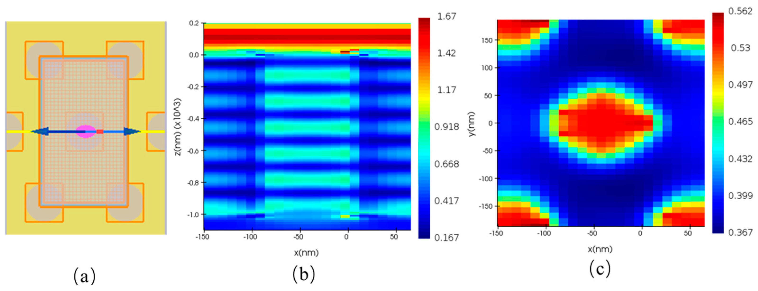
To verify whether the calculated results can achieve surface plasmon excitation, the obtained results were validated through simulation. Electromagnetic simulations of the designed MIM structure were performed using FDTD Solutions (2020 R2) simulation software. The material of the intermediate medium layer is set to be alumina. The material of the upper and lower layers is silver. The incident wavelength λ = 532 nm. The incident light propagates along the Z-axis direction. The symmetric and antisymmetric boundary conditions are set in the X- and Y-axis directions. The absorptive boundary condition (PML) is set in the Z-axis direction, and a grid of 1 nm × 1 nm × 1 nm size is set. The results are shown in Figure 3c, and it can be seen that there is an obvious enhancement effect in the holes of the model, which is the hot spot area in the figure.
Under 532 nm laser irradiation, an extremely strong electric field is concentrated near the small aperture on the output surface, exhibiting a typical localized field enhancement effect—an anomalous enhancement phenomenon characteristic of surface plasmon polaritons. A distinct standing wave phenomenon is also observed within the aperture. Simulation results confirm the successful surface plasmon excitation under 532 nm laser conditions, consistent with the computational predictions. According to the theoretical analysis above, both Au- and Ag-based MIM structures can be processed by the laser excitation of surface plasmas for the micro- and nano-etch processing of silicon wafers in the vicinity of a 216 nm cycle. So, under the same conditions as Ag/AAO/Ag, an FDTD simulation was also performed for the Au/AAO/Au structure. The intermediate dielectric layer material is alumina. The upper and lower layers are gold. The incident wavelength λ = 532 nm. The incident light propagates along the Z-axis direction. The symmetric and antisymmetric boundary conditions are set in the X and Y directions. The absorptive boundary condition (PML) is set in the Z direction, and a grid of 1 nm × 1 nm × 1 nm size is set. The results are shown in Figure 4c. It can be seen that there is an obvious enhancement effect in the holes of the model, which is the hot spot area in the figure. The energy of the surface plasmas produced by the laser-induced Au/AAO/Au structure is smaller than that of the surface plasmas produced by the laser-induced Ag/AAO/Ag structure, which proves that the Ag/AAO/Ag structure is more favorable for the excitation of surface plasmas. This is also why Ag/AAO/Ag was chosen over Au/AAO/Au for subsequent experiments in this paper.

2.2. Theoretical Analysis of Porous Anodized Aluminum Oxide Preparation

At present, the preparation process of AAO thin films has been relatively mature, and the pore size and pore period can be changed by changing the anodic oxidation process parameters [37,38,39]. However, the optimization of the process parameters using different acidic electrolytes is complicated. It is still necessary to carry out relevant experimental analyses and summarize the experimental methods for the electrolyte, as well as the oxidation voltage, oxidation time, and other relevant parameters. For AAO preparation, the oxidation voltage U has a linear relationship with the pore spacing, also known as the pore period, D of the AAO [38]:
D = ξ × U
where ξ takes the value of 2 to 2.5; for a pore spacing of 216 nm calculated according to Equation (6), it can be concluded that the anodizing voltage U ranges from approximately 89 V to 110 V. Anodized aluminum oxide templates can be prepared in a variety of electrolytes, such as oxalic acid, phosphoric acid, sulfuric acid, and their mixed electrolyte solutions. Each electrolyte solution has a corresponding maximum oxidation voltage: 100 V for the oxalic acid system, 195 V for the phosphoric acid system, and 25 V for the sulfuric acid system. Aluminum flakes exceeding the maximum oxidation voltage will produce an ablation phenomenon during anodic oxidation, which will affect the experimental results. The most suitable electrolyte solution in this voltage range is the oxalic acid solution, which prepares AAO with a regular and orderly structure and smaller pore size [40]. In summary, to achieve the specific goal of precisely preparing an AAO template with a pore period of 216 nm, we followed an optimization path that combined theoretical calculations with experimental verification. First, based on the linear relationship between pore spacing and voltage (Equation (6)), we calculated the theoretical voltage range (89–110 V). Then, after considering the characteristics of the electrolyte (the safe voltage of the oxalic acid system is ≤100 V), we designed an optimized experiment using a 0.3 molar/liter oxalic acid solution and anhydrous ethanol in a volume ratio of 4:1 as the electrolyte, and preparing AAO samples at three key voltage points of 95 V, 100 V, and 105 V. Through the characterization and analysis of the sample structure, we ultimately determined and verified the optimal anodic oxidation voltage value that could produce AAO samples with the target period (216 nm) and regular structure.

2.3. Theoretical Analysis of Laser Induction

A nanosecond laser is used as the light source for the induced excitation of surface plasmas, which operates at a wavelength of λ = 532 nm, with a maximum power of P = 15 W and a spot diameter of 50 microns. By changing the current size and pulse repetition frequency f, scanning speed v, filling spacing Ls, etc., the corresponding laser power and laser energy density can be obtained, and the relevant equations are shown below.
When irradiating with laser light in a preset unit area, the magnitude of the laser energy density accumulated in the area, Facc, can be obtained from the following Equation (7):
F a c c = E A = E p N p A
where A is the area of the scanning area and Np is the total number of laser pulses. Ep is the laser single-pulse energy. The output average power P, the relationship between the pulse repetition frequency f and the single pulse energy, and the value of the total number of pulses Np are shown in Equations (8) and (9):
E p = p f
N p = a f v × b L s = a b f v L s
where a and b are the length and width of the scanning area, respectively, v is the laser scanning speed, and Ls is the laser scanning spacing. From joint Equations (7)–(9), we can obtain the following:
F a c c = p f × a b f v L s = P v L s
From Equation (10), the output average power P mainly determines the laser energy density size Facc, laser scanning speed v, and laser scanning spacing Ls laser parameters. Different laser energy densities Facc are obtained by changing the above parameters.

3. Experimental Procedure

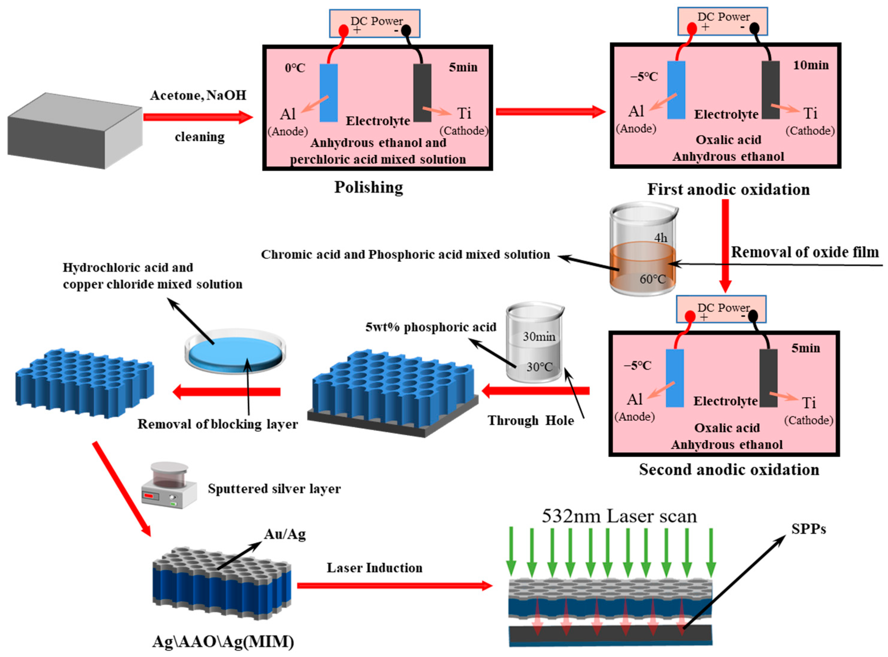
The overall experiment is divided into two parts: the preparation of AAO film and the processing of silicon nanoholes. The specific experimental flow is shown in Figure 5. The microscopic morphology of the experimental process was observed using field emission scanning electron microscope SEM (FEI Apreo; Thermo Fisher Scientific, Hillsboro, OR, USA; manufactured in Czech) and atomic force microscope (Bruker multimode8, Billerica, MA, USA).

3.1. Preparation of 216 nm MIM-Type Hole Array Cycles

Firstly, the aluminum sheet with 99.9999% purity was pre-treated by immersing it in acetone solution and cleaning it for 20 min using an ultrasonic cleaning apparatus to remove the surface grease and impurities. The cleaned aluminum sheet was immersed in 0.1 mol/L NaOH solution for 10 min to remove the dense oxide film. In the next step, the treated aluminum sheet was subjected to electrochemical polishing treatment in a mixed solution of anhydrous ethanol and perchloric acid at a volume ratio of 4:1, with an anodic oxidation voltage of 21 V and a reaction time of 5 min, to obtain an aluminum sheet with a mirror-like effect.
AAO films were prepared through the second oxidation method [41], and the solutions for both anodic oxidations were a mixture of 0.3 mol/L oxalic acid solution and anhydrous ethanol in a volume ratio of 4:1, at oxidation voltages of 95 V, 100 V, and 105 V, and an ambient temperature of minus 5 degrees Celsius, respectively. The first oxidation time was 10 min, and, after the completion of the first anodic oxidation, the aluminum sheets were submerged in a mixed solution of 0.2 mol/L chromic acid and 6 wt% phosphoric acid and placed in a water bath oven at an ambient temperature of 60 degrees Celsius for 4 h to remove the aluminum oxide generated by the first oxidation. A second anodizing was carried out in the same environment as the first anodizing.
The aluminum sheet obtained from the second anodizing was immersed in 5 wt% phosphoric acid solution in a water bath oven for reaming at an ambient temperature of 30 degrees Celsius for 30 min. Then, the aluminum sheet was immersed in a mixed hydrochloric acid–copper chloride solution and 5 wt% phosphoric acid to remove the aluminum matrix and the barrier layer to obtain the AAO film at ambient room temperature. Finally, a thin-film lens with an MIM-type structure (Ag/AAO/Ag) can be obtained after sputtering a layer of silver on each of the front and back surfaces of AAO using an ion sputtering apparatus.

3.2. Laser-Induced Surface Plasmas for Nanopore Etching of Single Crystal Silicon

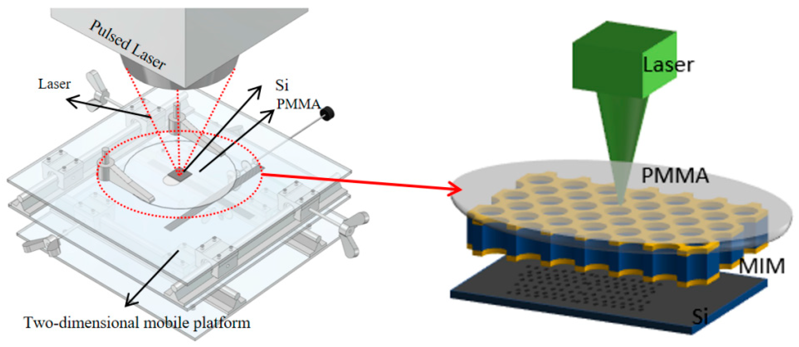
The whole experimental process is based on the experimental requirements. In order to carry out the experimental processing more rigorously, a set of processing platforms for surface plasma lithography is designed, and the specific structure of the platform is shown in Figure 6. We chose 10 mm × 10 mm polished single crystal silicon as the surface to be processed. During the processing, the silicon wafer to be processed is not closely integrated with the MIM structure, which will cause the generated SPPs to undergo attenuation and then propagate to the surface of the silicon wafer. Therefore, by placing poly methyl methacrylate (PMMA) above the MIM, the MIM and the silicon wafer can be closely connected, reducing the exponential attenuation of SPPs in the air. Compared with glass, PMMA has a higher light transmittance and impact resistance, making it more suitable for this experiment. The processing light source was selected as the green light source with a wavelength of 532 nm. The maximum output power was 15 W. The spot diameter was 50 microns. The laser processing area was set to be 2 mm × 2 mm. The laser pulse frequency was 20 KHz. The release time was 5 us. The focal length of 224 mm was chosen for the preliminary experiments. A laser power meter was used to measure the power size of the laser using different parameters. The measurement range of the power meter is lower than 60 W, and continuous measurement power is lower than 30 W. We measured the laser energy power under different currents with a laser pulse frequency of 20 KHz, release time of 5 us, laser scanning spacing of 0.01 mm, and scanning speeds of 2000 mm/s and 3000 mm/s, respectively, and the specific energy power values are shown in Figure 7. Compared to the scanning speed of 2000 mm/s, the scanning speed of 3000 mm/s scans a longer distance at the same time.
As a result, the laser energy over the same area will be distributed over a larger area, resulting in a lower energy density per unit area. An increase in energy density provides enough energy to cause electrons to dissociate from the solid surface and form a plasma. Higher energy densities provide more energy, resulting in more electrons dissociating and participating in plasma formation. Therefore, an increase in energy density increases the density of the surface plasmas and causes the temperature of the surface plasma to rise, increasing the thermal energy within the plasma. Excessive energy density will lead to some negative effects, such as thermal damage, melting, evaporation, or oxidation of the material. In summary, a scanning speed of 2000 mm/s was selected for the initial experiments. The laser power was further varied by adjusting the current parameter during the experiments to fine-tune the laser energy density. Different laser accumulation energy densities were obtained to achieve the excitation of surface plasma for the preparation of nanoholes on the surface of silicon wafers [42].

4. Results

4.1. Preparation of AAO Thin Films and MIM Structure Characterization and Analysis

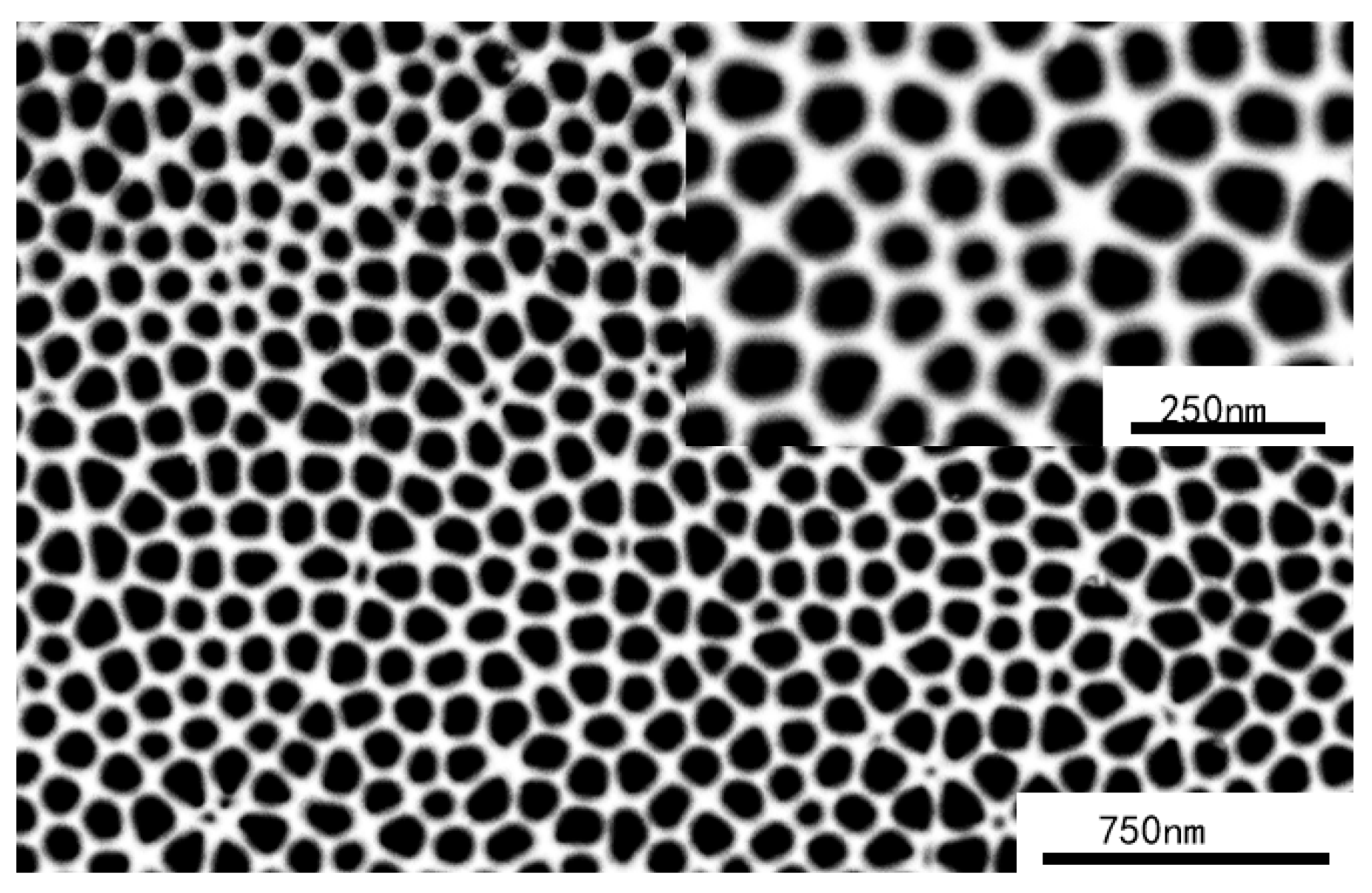
The results of AAO film preparation are shown in Figure 8. A mixture of 0.3 mol/L oxalic acid solution and anhydrous ethanol with a volume ratio of 4:1 was used as the electrolyte. The porous anodic alumina pore period was varied by comparing the porous anodic alumina pore period at voltages of 95 V, 100 V, and 105 V with the specific parameters shown in Table 1.
We found that the periodic hole spacing of AAO films increased with increasing voltage, which is in accordance with the theoretical analysis above. It is confirmed that an anodic oxidation at 105 V can achieve the preparation of a hole cycle of about 216 nm. In the next step, the second anodizing time was adjusted to further reduce the thickness of the AAO film without affecting its regularity. As shown in Figure 9, the second anodizing time was adjusted from 10 to 5 min to reduce the AAO thickness from 13,612 nm to 4584 nm. Figure 10 shows the SEM surface topography of the AAO film at a 216 nm cycle after the blocking layer completely disappeared after 60 min of hole passing. Finally, an ordered Ag/AAO/Ag (MIM-type) periodic hole array structure can be obtained by sputtering a layer of silver on both the front and back surfaces of the ion-sputtering instrument. The ion sputtering instrument with an ion current of 10 mA, a cathode voltage of −1.6 KV, and a sputtering time of 1 min 30 s sputtered a layer of silver with a thickness of about 250 nm on the surface of the AAO film. The specific morphology is shown in Figure 11. From Figure 11, it can be observed that the sputtered silver layer does not form a completely continuous film, but tends to accumulate at the edges and tips of the AAO nanopores, forming discrete nanoclusters [43]. At the sharp tips of the highly curved nanostructures, due to a higher surface energy and stronger local electric field, metal atoms are more likely to migrate and nucleate and grow, thereby leading to the formation of selective clusters [44,45]. This self-assembly structure of metal nanoclusters is precisely the key structure relied upon by sensing technologies based on plasmon excitation effects such as surface-enhanced Raman scattering. The nano-gaps between the clusters can generate extremely strong local electromagnetic field enhancements, known as “hot spots”, which can significantly enhance the optical signals of the molecules nearby [46]. Also, compared with Figure 10, it can be seen that the metallic luster of the AAO sputtered with a layer of silver is more obvious. There are obviously visible particles, which makes the MIM structure pore size smaller, and the sputtered silver film does not change the periodic pore spacing of the AAO membrane.

4.2. Results and Analysis of Micro- and Nanopore Preparation by Laser Irradiation of Ag/AAO/Ag Periodic Pore Arrays for Excitation of SPPs

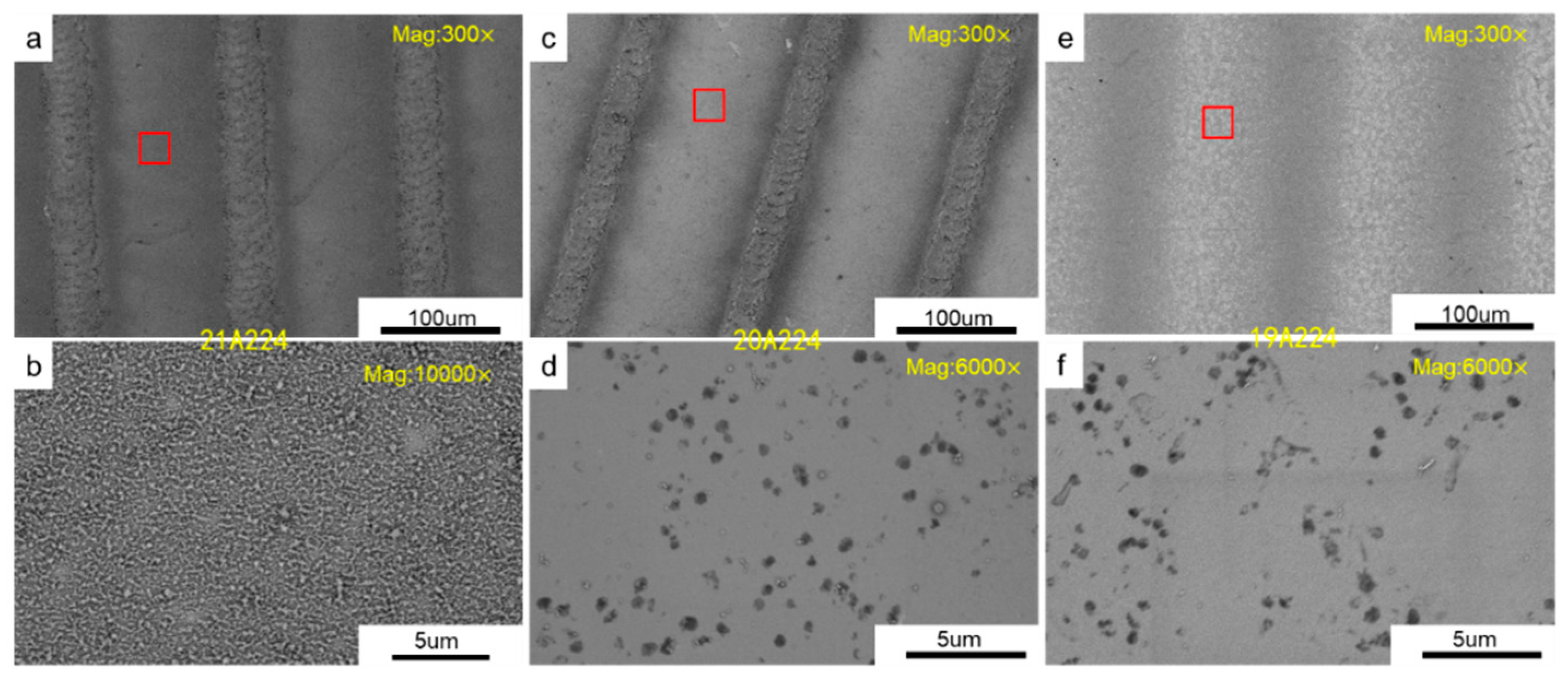
When the laser is irradiated on the MIM periodic thin-film structure, a localized electric field enhancement will be generated on the surface of the mask’s periodic hole array. It shows the above simulation hotspot diagram, manifested by the generation of SPPs and their undirected propagation on the surface of the silver layer of the MIM structure. Since the silicon wafer to be processed is immediately below the MIM structure, this provides sufficient conditions for the SPPs to propagate and act on the surface of the single-crystal silicon wafer. The SPPs are propagated perpendicular to the surface along the periodic holes to act on the silicon surface to process the nanopores. We first used a scanning speed of 2000 mm/s at a laser focal length of 224 mm. According to the laser power data measured above, the preliminary experimental test was carried out under the current of 19 A~21 A. The results are shown in Figure 12, where Figure 12a,c,e correspond to the surface morphology SEM images of micro–nanopores prepared on the surface of silicon wafers through the induced excitation of SPPs with the current parameters of 21 A~19 A under the laser focal length of 224 mm, respectively, and Figure 12b,d,f are the high-magnification SEM images of the square areas in Figure 12a,c,e, respectively.
By comparing the images in Figure 12a,c,e, it can be seen that the laser focusing process will leave obvious etching traces on the surface of the wafer. The depth of the traces gradually becomes lighter as the current decreases, which is in line with the trend of the laser power change in Figure 6. In Figure 12b, it can be seen that, at a current of 21 A, the part of the wafer in the middle of the two etching traces has also been completely destroyed by ablation. However, in Figure 12f, although the silicon wafer has slight ablation traces, many nanometer-sized holes can be observed in the middle of the etch traces, which initially proves the feasibility of the theoretical experiment above. The following needs to consider the problem of etching traces, as can be seen by comparing the pictures; the traces can be avoided by further reducing the current. However, considering that a further current reduction will lead to too low of a processing power and thus affect the hole effect, we intend to avoid the traces by utilizing defocused processing. This is because the small spot diameter in laser focal processing leads to a high energy density per unit of laser light, which will inevitably leave etching marks when processing nanoholes.
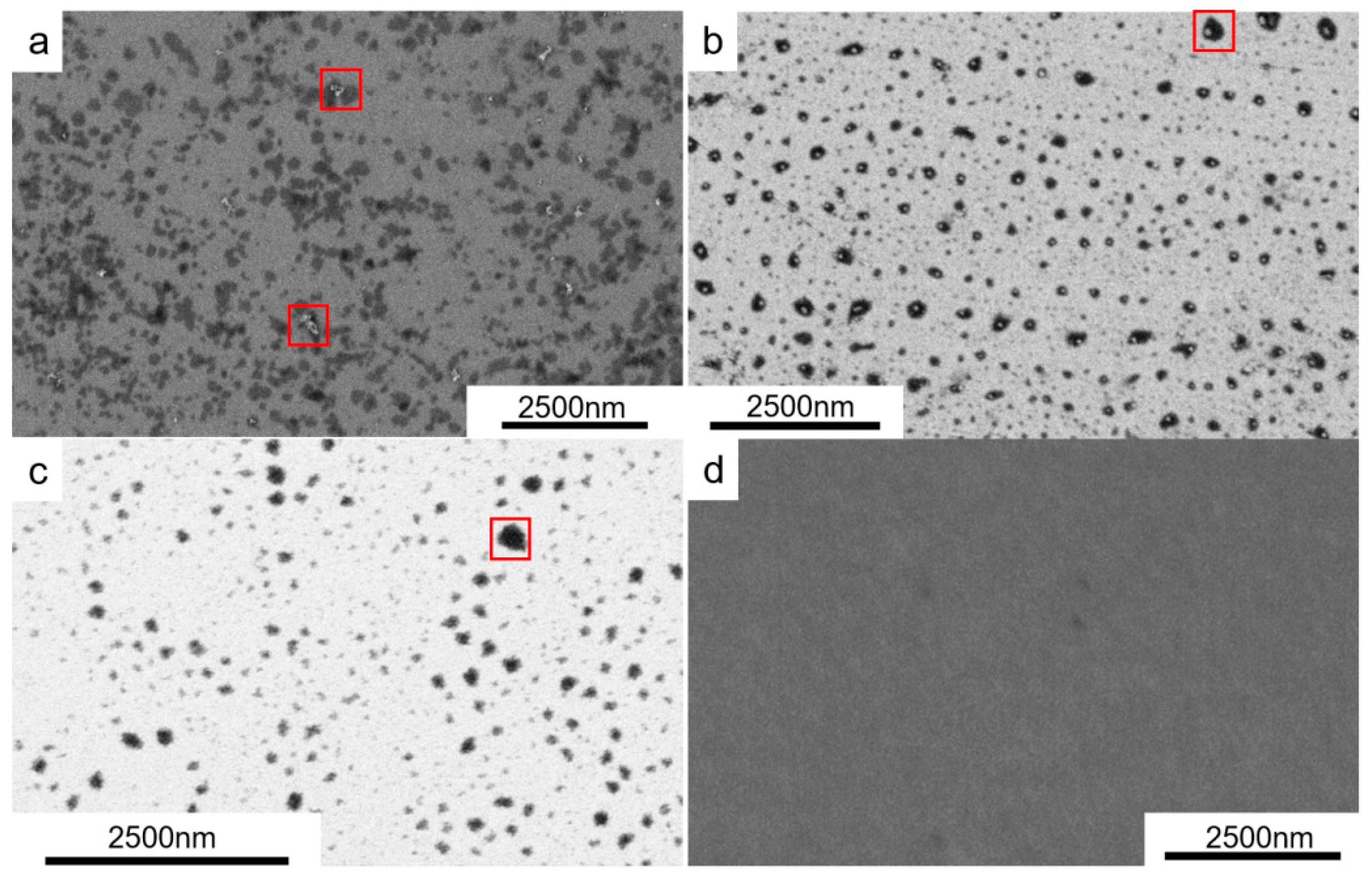
The experiments were optimized to process the silicon wafers at a processing distance of 200 mm using an off-focus laser processing method. The generation of etch marks was successfully avoided by changing the processing method. Many small nanoscale holes were observed on the wafer surface. The lowest diameter of the holes is about 70 nm. The average diameter is about 120 nm. The hole spacing fluctuates from 150 to 300 nm, showing a more uniform distribution effect on the wafer surface. Preliminarily, the parameters of the etched holes are more related to the prepared MIM structure. However, due to the process of preparing AAO films, which are usually affected by temperature, voltage perturbation, and other factors, the pore size of the film will appear to have a diameter size, pore spacing, and spatial distribution that is not entirely regular. This leads to the situation in Figure 13b, where more regular holes are etched in the middle part, but no holes are etched in the square area. Due to the above-mentioned reasons, the SPPs show an exponential decay in air. In the process, the wafer to be processed is not closely combined with the MIM structure. There is inevitably a gap between the two, resulting in the SPPs generated by the excitation being attenuated and then propagated to the surface of the wafer. The range of the field strength and the energy size will be further reduced, affecting the size of the processed hole and the distribution of the hole diameter. However, a current that is too large can also lead to a field strength that is too high. The etched holes are connected together, and impurities are generated on the silicon surface, as shown in Figure 13a.
According to Figure 14, the number of holes in the same area increases as the current number increases. Comparing Figure 14b,c, the holes in Figure 14a are the most numerous, and a considerable number of holes are connected together. There are many large particles of impurities produced on the silicon surface, as shown in the square area in the figure. The holes in Figure 14b,c gradually decrease as the current decreases, the laser power decreases, and thus the energy density decreases. Figure 14c shows that the processed holes do not produce the accompanying impurities. The impurities are the bright particles evident in the figure, with different sizes of particles, which are formed by laser irradiation on the Ag/AAO/Ag periodic structure, inducing the excitation of the surface plasma wave propagating on the surface of the silver layer, which produces a transient high temperature that causes some silver particles in the surface layer to melt rapidly, and then condense to form the silver particles quickly when they fall onto the surface of the silicon wafer. As the laser energy increases, the generation of particle impurities increases. Finding the balance between the hole etching effect and impurity generation and trying to avoid the formation of silver particles on the sample surface can be realized by adjusting the laser parameters.
In order to more intuitively understand the overall distribution characteristics of the nanopore size data, Figure 14 was processed and analyzed using ImageJ(Fiji) software to measure the size and number of tiny pores under different current parameters, respectively. In order to investigate further and compare the differences in pore size distributions between different samples and eliminate some random errors, a Gaussian fitting process was performed on the data to predict the probability distribution of unmeasured pore size values. It is worth noting that, for the pore size distribution histogram at 23 A, we performed a bimodal Gaussian fit. As shown in Figure 14, at 23 A, numerous pores are present on the silicon wafer, and a significant number of these pores have coalesced. This results in the emergence of a second peak between 150 nm and 190 nm under the 23 A condition. The curves are shown in Figure 15, which shows that, as the current increases, the energy density of the laser increases, resulting in a gradual increase in the diameter of the holes processed.
To prove that the plasma effect generates the nanoholes on the surface of the silicon wafer, we used AAO film instead of the MIM structure with the exact parameters of the silicon wafer processing. At this time, due to the absence of metallic silver as the raw material to stimulate the surface of the plasma, according to the theory, the silicon surface cannot be processed out of the traces. The result is shown in Figure 14d, which is the surface topography of the silicon surface directly irradiated by a laser under a 23 A current without using the MIM structure mask, and the surface is relatively smooth, without processing traces. The whole process of nanohole etching can be regarded as removing and reorganizing materials. During the whole process, the laser-induced excitation of surface plasma is first used so that the local electric field on the surface of the silicon wafer is enhanced, which leads to an increase in temperature. The plasma-induced enhanced electric field, Equation (11), and the temperature increment, Equation (12), can be calculated to show that the temperature of the silicon surface during the process can reach more than 2000 K [47], which is enough to provide the necessary conditions for the etching of the holes. In Equations (11) and (12), I0 is the incident intensity of the optical field. n is the ratio of the dielectric constant between the MIM structural mask and the substrate silicon. The constant A is the shape parameter of the mask. g2 is the increment of the field strength (~150). R is the radius of the mask aperture (~150 nm). F is the laser energy density. θ is the angle of incidence, equal to zero. k is the substrate silicon’s thermal conductivity (126 W/mk). t is the pulse width (t = 2 us).
I = I 0 [ 1 + ( n 1 ) A ] 2 = I 0 g 2
Δ T s u b s t r a t e = ( π R g 2 F cos θ 8 k t ) 1 2
We used a Multimode 8 atomic force microscope (AFM) from Bruker, Inc., and scanned the silicon wafer surface in the tap mode to investigate the depth characteristics of the processed holes. Figure 15 shows the AFM images of micro- and nanoholes prepared on the wafer surface, using laser-biased focus-induced SPPs at a processing distance of 200 mm and a current of 21 A, and the corresponding depth histograms. This experimental conditions correspond to Figure 14b. The maximum depth of the holes reaches 27.8 nm in the detection region, located in the square area marked in the figure. As can be observed from the image, the detection region is subjected to the highest energy, and, therefore, the deepest holes are processed in this region, accompanied by larger particles. Through the 3D image, we can clearly see the presence of larger particles above the deeper holes, and the maximum height of the particles is about 50 nm. This phenomenon verifies that the generation of particulate impurities is due to excessive energy and that these particulate impurities are the incidental products of the process of processing the holes. Considering the histogram data in Figure 15 and Figure 16 together, it can be concluded that most of the holes obtained by machining have depths between 2 and 5 nm and diameters in the range of about 90 to 130 nm. The above experimental results provide essential information about the depth characteristics of micro- and nanoholes in silicon wafers prepared using laser defocus-induced SPPs. These findings deepen our understanding of the relationship between pore properties and particle impurity generation during this process. This study provides valuable data and insights for further exploration in related fields.

5. Conclusions

Through research on the preparation of porous AAO films via the anodic oxidation method, we found that, using a mixed solution containing 0.3 mol/L oxalic acid and anhydrous ethanol (volume ratio 4:1) as the electrolyte, an AAO film with an average pore spacing of approximately 223 nm and a thickness of about 4500 nm could be prepared at an anodic oxidation voltage of 105 V. This result indicates that parameters such as electrolyte composition, anodic oxidation voltage, and through-hole time collectively influence the pore spacing of the fabricated AAO. After constructing the Ag/AAO/Ag metal–insulator–metal structure, we observed that this composite template effectively excites SPPs under 532 nm nanosecond laser irradiation, enabling fine hole etching on the single-crystal silicon surface with diameters as small as 50 nm and depths of approximately 27.8 nm. This phenomenon demonstrates that the Ag/AAO/Ag structure can efficiently excite surface plasmons, enabling micropore etching on single-crystal silicon. Furthermore, the impurity particles observed in the experiment may originate from metal agglomeration during sputtering or AAO surface inhomogeneities, suggesting that a further optimization of interface quality control is required in subsequent processes.
In conclusion, this study serves as a proof-of-concept demonstration that the Ag/AAO/Ag (MIM) periodic hole array composite structure can harness incident light to excite localized surface plasmons for etching micro- and nanoholes. Our findings establish the foundational principle and provide an essential reference for exploring this plasmon-assisted lithography technique for fabricating subwavelength structures.
The silver nanocluster structure observed in our experiments, while deviating from an ideal continuous film, serendipitously reveals an alternative pathway for potential application in plasmon sensing due to the formation of “hot spots”.
Looking forward, this nascent technology requires dedicated efforts to mature. Future work will therefore focus on two critical fronts to bridge the gap from concept to practical application: first, systematically optimizing anodic oxidation process parameters (such as voltage, temperature, and electrolyte composition) to achieve highly ordered nanochannel arrays can provide a more ideal structural foundation for plasmonic applications; second, by optimizing the deposition parameters to obtain a more uniform film or actively utilizing and regulating this self-organized cluster structure, a high-performance plasmonic “hot spot” array can be constructed for the high-sensitivity detection of biochemical molecules. Addressing these challenges will be crucial to assess the full potential and scalability of this method for achieving ordered pore structures on substrates like silicon.

Author Contributions

Conceptualization, S.H. and J.Z.; methodology, S.H., S.L. and J.Z.; software, W.M.; validation, R.W., Z.G. and Y.C.; formal analysis, S.H. and J.Z.; investigation, W.M.; resources. J.Z. and Z.G.; data curation, S.H., S.L. and R.W.; writing—original draft preparation, S.H.; writing—review and editing, J.Z. and Y.C.; visualization, S.H. and Z.G.; supervision, J.Z. and Z.G.; project administration, J.Z.; funding acquisition, J.Z. All authors have read and agreed to the published version of the manuscript.

Funding

This research received no external funding.

Institutional Review Board Statement

Not appliable.

Informed Consent Statement

Not appliable.

Data Availability Statement

Data will be made available on request.

Acknowledgments

The authors would like to gratefully acknowledge the financial support provided by Tianjin Municipal Education Commission, China, under the Grant 2017KJ020. Financial support from Tianjin Municipal Science and Technology Commission, China, under Grant 17JCYBJC42400 is appreciated. This work also has been supported by Tianjin Key Laboratory of Integrated Design and On-line Monitoring for Light Industry & Food Machinery and Equipment, Grant No. 2019LIMFE08.

Conflicts of Interest

Author Sipeng Luo was employed by the company Shenyang SIASUN Robot & Automation Co., Ltd. The remaining authors declare that the research was conducted in the absence of any commercial or financial relationships that could be construed as a potential conflict of interest”.

Abbreviations

The following abbreviations are used in this manuscript:
AAOAnodic aluminum oxide
Ag/AAO/AgSilver–alumina–silver
Au/AAO/AuGold–alumina–gold
MIMMetal–insulator–metal
SPPsSurface plasmon polaritons
SPsSurface plasmons

References

  1. Wang, K.; Liu, C.; Meng, T.; Yi, C.; Gong, X. Inverted organic photovoltaic cells. Chem. Soc. Rev. 2016, 45, 2937–2975. [Google Scholar] [CrossRef]
  2. Duan, C.; Wang, W.; Xie, Q. Fabrication of nanofluidic devices. Biomicrofluidics 2013, 7, 026501. [Google Scholar] [CrossRef]
  3. Gilboa, T.; Zvuloni, E.; Zrehen, A.; Squires, A.H.; Meller, A. Automated, ultra-fast laser-drilling of nanometer scale pores and nanopore arrays in aqueous solutions. Adv. Funct. Mater. 2020, 30, 1900642. [Google Scholar] [CrossRef]
  4. Lillo, M.; Losic, D. Ion-beam pore opening of porous anodic alumina: The formation of single nanopore and nanopore arrays. Mater. Lett. 2009, 63, 457–460. [Google Scholar] [CrossRef]
  5. Knapp, J.A.; de Boer, M.P. Mechanics of microcantilever beams subject to combined electrostatic and adhesive forces. J. Microelectromech. Syst. 2002, 11, 754–764. [Google Scholar] [CrossRef]
  6. Biapo, U.; Ghisolfi, A.; Gerer, G.; Spitzer, D.; Keller, V.; Cottineau, T. Functionalized TiO2 Nanorods on a Microcantilever for the Detection of Organophosphorus Chemical Agents in Air. ACS Appl. Mater. Interfaces 2019, 11, 35122–35131. [Google Scholar] [CrossRef]
  7. Liu, N.W.; Liu, C.Y.; Wang, H.H.; Hsu, C.F.; Lai, M.Y.; Chuang, T.H.; Wang, Y.L. Focused-Ion-Beam-Based Selective Closing and Opening of Anodic Alumina Nanochannels for the Growth of Nanowire Arrays Comprising Multiple Elements. Adv. Mater. 2008, 20, 2547–2551. [Google Scholar] [CrossRef]
  8. Chen, B.; Lu, K.; Tian, Z. Novel patterns by focused ion beam guided anodization. Langmuir 2011, 27, 800–808. [Google Scholar] [CrossRef] [PubMed]
  9. Howitt, D.G.; Chen, S.J.; Gierhart, B.C.; Smith, R.L.; Collins, S.D. The electron beam hole drilling of silicon nitride thin films. J. Appl. Phys. 2008, 103, 024310. [Google Scholar] [CrossRef]
  10. Ammann, A.A. Inductively coupled plasma mass spectrometry (ICP MS): A versatile tool. J. Mass Spectrom. 2007, 42, 419–427. [Google Scholar] [CrossRef] [PubMed]
  11. Henzie, J.; Lee, M.H.; Odom, T.W. Multiscale patterning of plasmonic metamaterials. Nat. Nanotechnol. 2007, 2, 549–554. [Google Scholar] [CrossRef]
  12. Ritchie, R.H. Plasma. losses by fast electrons in thin films. Phys. Rec. 1957, 106, 874–875. [Google Scholar] [CrossRef]
  13. Stem, E.A.; Ferrel, R.A. Surface Plasma oseillations of degenerate electron gas. Phys. Rev. B 1960, 120, 130–131. [Google Scholar]
  14. Barnes, W.L.; Dereux, A.; Ebbesen, T.W. Surface plasmon subwavelength optics. Nature 2003, 424, 824–830. [Google Scholar] [CrossRef]
  15. Ozbay, E. Plasmonics: Merging photonics and electronics at nanoscale dimensions. Science 2006, 311, 189–193. [Google Scholar] [CrossRef] [PubMed]
  16. Tong, L.; Wei, H.; Zhang, S.; Xu, H. Recent advances in plasmonic sensors. Sensors 2014, 14, 7959–7973. [Google Scholar] [CrossRef] [PubMed]
  17. Piliarik, M.; Homola, J.; Manikova, Z.; Ctyroky, J. Surface plasmon resonance sensor based on a single-mode polarization-maintaining optical fiber. Sens. Actuators B Chem. 2003, 90, 236–242. [Google Scholar] [CrossRef]
  18. Hajshahvaladi, L.; Kaatuzian, H.; Danaie, M. A high-sensitivity refractive index biosensor based on Si nanorings coupled to plasmonic nanohole arrays for glucose detection in water solution. Opt. Commun. 2021, 502, 127421. [Google Scholar] [CrossRef]
  19. Alipour, A.; Farmani, A.; Mir, A. High Sensitivity and Tunable Nanoscale Sensor Based on Plasmon-Induced Transparency in Plasmonic Metasurface. IEEE Sens. J. 2018, 18, 7047–7054. [Google Scholar] [CrossRef]
  20. Liu, L.; Luo, Y.; Zhao, Z.; Zhang, W.; Gao, G.; Zeng, B.; Wang, C.; Luo, X. Large area and deep sub-wavelength interference lithography employing odd surface plasmon modes. Sci. Rep. 2016, 6, 30450. [Google Scholar] [CrossRef]
  21. Fang, N.; Lee, H.; Sun, C.; Zhang, X. Sub-Diffraction-Limited Optical Imaging with a Silver Superlens. Science 2005, 308, 534–537. [Google Scholar] [CrossRef]
  22. Liu, Z.; Lee, H.; Xiong, Y.; Sun, C.; Zhang, X. Far-Field Optical Hyperlens Magnifying Sub-Diffraction-Limited Objects. Science 2007, 315, 1686. [Google Scholar] [CrossRef]
  23. Schilling, A.; Schilling, J.; Reinhardt, C.; Chichkov, B. A superlens for the deep ultraviolet. Appl. Phys. Lett. 2009, 95, 121909. [Google Scholar] [CrossRef]
  24. Kletchillann, E. The determination of the optical constants of metals by exciation of surface plasmons. Z. Phys. A Hadron. Nucl. 1971, 241, 313–315. [Google Scholar]
  25. Wang, C.; Du, C.; Lv, Y.; Luo, X. Surface electromagnetic wave excitation and diffraction by subwavelength slit with periodically patterned metallic grooves. Opt. Express 2006, 14, 5671–5681. [Google Scholar] [CrossRef]
  26. Otto, A. Excitation of Nonradiative surface Plasmon wave in sliver by the method of frustrated total reflection. Z. Phys. A Hadron. Nucl. 1968, 205, 398–399. [Google Scholar] [CrossRef]
  27. Yan, S.; Zhang, M.; Zhao, X.; Zhang, Y.; Wang, J.; Jin, W. Refractive Index Sensor Based on a Metal–Insulator–Metal Waveguide Coupled with a Symmetric Structure. Sensors 2017, 17, 2879. [Google Scholar] [CrossRef] [PubMed]
  28. Jani, A.M.M.; Losic, D.; Voelcker, N.H. Nanoporous anodic aluminium oxide: Advances in surface engineering and emerging applications. Prog. Mater. Sci. 2013, 58, 636–704. [Google Scholar] [CrossRef]
  29. Lee, W.; Ji, R.; Gösele, U.; Nielsch, K. Fast fabrication of long-range ordered porous alumina membranes by hard anodization. Nat. Mater. 2006, 5, 741–747. [Google Scholar] [CrossRef]
  30. Miao, W.; Yang, Y.; Zhao, J.; Zhang, H.; Guo, Z.; Cui, Y.; Wang, R.; Zhu, Y. Fabrication of Au/AAO/Au nanopore arrays based on induced excitation SPPs for the fabrication of nanopores on silicon surfaces. Mater. Today Commun. 2023, 35, 105953. [Google Scholar] [CrossRef]
  31. Huang, Z.; Geyer, N.; Werner, P.; De Boor, J.; Gösele, U. Metal-assisted chemical etching of silicon: A review: In memory of Prof. Ulrich Gösele. Adv. Mater. 2011, 23, 285–308. [Google Scholar] [CrossRef]
  32. Majumdar, P.; Ray, A. Maxwell electrodynamics in terms of physical potentials. Symmetry 2019, 11, 915. [Google Scholar] [CrossRef]
  33. Tarigan, H.J. Study of Surface Plasmon Polaritons (SPPs) Propagation Through Plasmonic Crystals. Master’s Thesis, Texas Tech University, Lubbock, TX, USA, May 2012. [Google Scholar]
  34. Wang, G.; Lu, H.; Liu, X. Dispersionless slow light in MIM waveguide based on a plasmonic analogue of electromagnetically induced transparency. Opt. Express 2012, 20, 20902–20907. [Google Scholar] [CrossRef]
  35. Dong, J.; Liu, J.; Kang, G.; Xie, J.; Wang, Y. Pushing the resolution of photolithography down to 15nm by surface plasmon interference. Sci. Rep. 2014, 4, 5618. [Google Scholar] [CrossRef] [PubMed]
  36. Xie, H.; Kong, F.M.; Li, K. The Electric Field Enhancement and Resonance in Optical Antenna Composed of AU Nanoparicles. J. Electromagn. Waves Appl. 2009, 23, 534–547. [Google Scholar] [CrossRef]
  37. Belwalkar, A.; Grasing, E.; Vangeertruyden, W.; Huang, Z.; Misiolek, W. Effect of processing parameters on pore structure and thickness of anodic aluminum oxide (AAO) tubular membranes. J. Membr. Sci. 2008, 319, 192–198. [Google Scholar] [CrossRef] [PubMed]
  38. Lee, W.; Park, S.J. Porous anodic aluminum oxide: Anodization and templated synthesis of functional nanostructures. Chem. Rev. 2014, 114, 7487–7556. [Google Scholar] [CrossRef]
  39. Sulka, G.D.; Stępniowski, W.J. Structural features of self-organized nanopore arrays formed by anodization of aluminum in oxalic acid at relatively high temperatures. Electrochim. Acta 2009, 54, 3683–3691. [Google Scholar] [CrossRef]
  40. Reddy, P.R.; Ajith, K.M.; Udayashankar, N.K. Optical and mechanical studies on free standing amorphous anodic porous alumina formed in oxalic and sulphuric acid. Appl. Phys. A 2018, 124, 765. [Google Scholar] [CrossRef]
  41. Yuan, J.H.; He, F.Y.; Sun, D.C.; Xia, X.H. A Simple Method for Preparation of Through-Hole Porous Anodic Alumina Membrane. Chem. Mater. 2004, 16, 1841–1844. [Google Scholar] [CrossRef]
  42. Rieger, G.; Taschuk, M.; Tsui, Y.; Fedosejevs, R. Comparative study of laser-induced plasma emission from microjoule picosecond and nanosecond KrF-laser pulses. Spectrochim. Acta Part B At. Spectrosc. 2003, 58, 497–510. [Google Scholar] [CrossRef]
  43. Xu, Y.; Zhang, J.; Liang, F.; Yin, M.; He, M. Investigation of magnetron sputtered nano-silver coating on titanium surface with micro-nanostructure. Surfaces Interfaces 2023, 38, 102770. [Google Scholar] [CrossRef]
  44. Yue, Y.; Yan, X.; Zhang, Y. Nano-fiber-structured Cantor alloy films prepared by sputtering. J. Mater. Res. Technol. 2022, 21, 1120–1127. [Google Scholar] [CrossRef]
  45. Tran, T.; Wang, X.; Shrestha, M.; Wang, K.; Fan, Q.H. Ultra-thin silver films grown by sputtering with a soft ion beam-treated intermediate layer. J. Phys. D Appl. Phys. 2023, 56, 365501. [Google Scholar] [CrossRef]
  46. Vilkevičius, K.; Ignatjev, I.; Selskis, A.; Niaura, G.; Stankevičius, E. Tuning SERS performance through the laser-induced morphology changes of gold nanostructures. Appl. Surf. Sci. 2024, 660, 160003. [Google Scholar] [CrossRef]
  47. Molian, P.A. Laser-Energized Plasmonics for Nanopatterning Medical Devices. J. Micro Nano-Manuf. 2015, 3, 031003. [Google Scholar] [CrossRef]
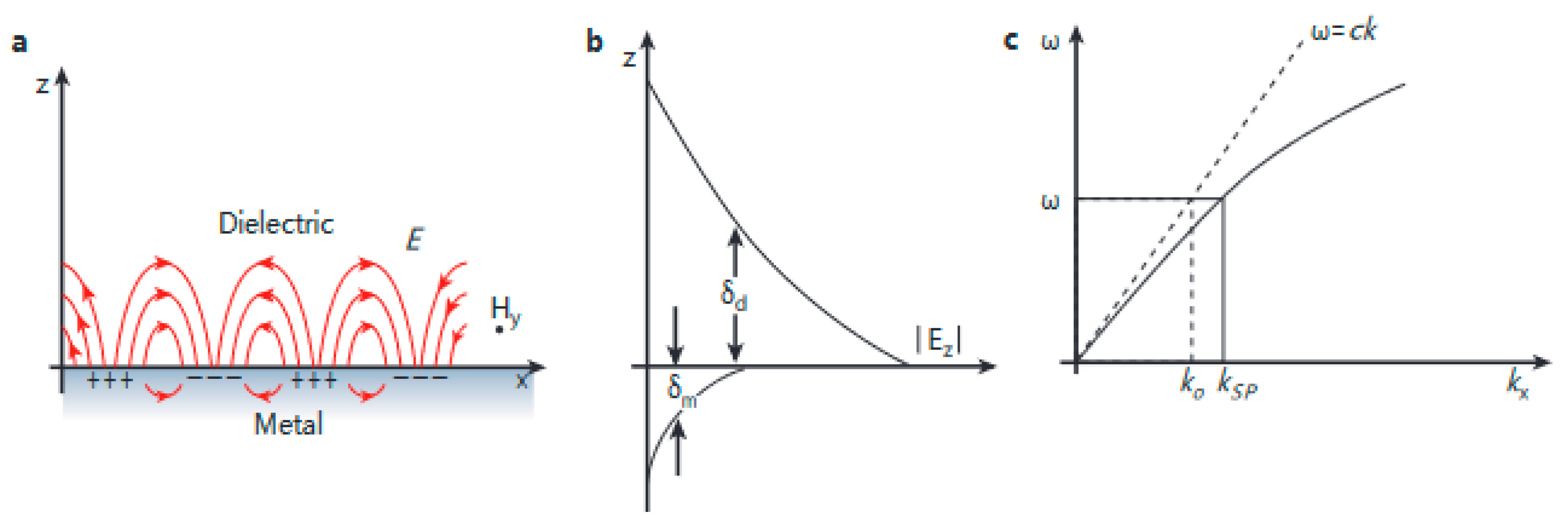
Figure 1. (a) Two-dimensional component plot of the electric and magnetic fields of photons on a metal surface; (b) component plot of the electric field on a vertical surface; (c) SP dispersion curve [14].
Coatings 15 01187 g001
Figure 2. Dielectric constants of silver and alumina materials in FDTD at 532 nm laser wavelength.
Coatings 15 01187 g002
Figure 3. (a) Schematic diagram of the simulation of the X-Y plane of the Ag/AAO/Ag structure; (b) field intensity distribution of the X-Z plane of the Ag/AAO/Ag structure; (c) field intensity distribution of the X-Y plane of the Ag/AAO/Ag structure.
Coatings 15 01187 g003
Figure 4. (a) Schematic diagram of the simulation of the X-Y surface of the Au/AAO/Au structure; (b) field intensity distribution of the X-Z surface of the Au/AAO/Au structure; (c) field intensity distribution of the X-Y surface of the Au/AAO/Au structure.
Coatings 15 01187 g004
Figure 5. Flowchart of the overall experiment.
Coatings 15 01187 g005
Figure 6. Schematic of the machining platform and laser processing.
Coatings 15 01187 g006
Figure 7. Power diagram of laser energy at different currents.
Coatings 15 01187 g007
Figure 8. (a) The average pore spacing of AAO prepared at an anodic oxidation voltage of 105 V is about 217 nm without a through-hole. (b) The average pore spacing of AAO prepared at an anodic oxidation voltage of 95 Vis is about 189 nm. (c) The average pore spacing of AAO prepared at an anodic oxidation voltage of 100 V is about 203 nm.
Coatings 15 01187 g008
Figure 9. (a) SEM image of AAO cross-section for 10 min of first anodizing and 10 min of second anodizing; (b) SEM image of AAO cross-section for 10 min of first anodizing and 5 min of second anodizing.
Coatings 15 01187 g009
Figure 10. SEM image of AAO with the period of 216.95 nm and average pore size of 117.64 nm.
Coatings 15 01187 g010
Figure 11. Surface morphology and cross-sectional SEM image of a sputtered silver layer of 216 nm periodic hole spacing AAO film.
Coatings 15 01187 g011
Figure 12. Surface SEM morphology of nanopores prepared on silicon wafer surface by laser focusing-induced excitation of SPPs at 224 mm processing distance. (a,c,e) show the SEM images of the silicon surface processed with 21 A~19 A currents, respectively; (b,d,f) are enlarged SEM images of the square region in (a) (c) (e), respectively.
Coatings 15 01187 g012
Figure 13. SEM image of surface morphology defects of nanopores prepared on the surface of silicon wafers by laser defocus-induced excitation of SPPs at 200 mm processing distance. (a) Impurities form on the surface of silicon wafers.; (b) Uneven etching on the surface of the silicon wafer.
Coatings 15 01187 g013
Figure 14. SEM images of the surface morphology of nanopores prepared on the surface of silicon wafers by laser defocus-induced excitation of SPPs at 200 mm processing distance. (ac) show the SEM images of the processed silicon surface at 23 A, 21 A, and 19 A currents, respectively; (d) shows the surface morphology of the silicon surface directly irradiated by the laser at 23 A current without the use of MIM structure mask.
Coatings 15 01187 g014
Figure 15. Pore size distribution of nanopores prepared at currents 19 A~23 A.
Coatings 15 01187 g015
Figure 16. Surface AFM map and depth histogram of micro- and nanopores prepared on the surface of silicon wafers at 200 mm processing distance and current of 21 A.
Coatings 15 01187 g016
Table 1. Oxidation time, average pore spacing, and thickness of AAO prepared at oxidation voltage of 95 V to 105 V under electrolyte of 0.3 mol/L oxalic acid solution.
Voltage
(V)
Primary Oxidation Time (min)Secondary Oxidation Time (min)Hole Spacing
(nm)
Nanopore
(nm)
951010189 (±3)150 (±3)
1001010203 (±3)147 (±3)
1051010217 (±5)117 (±5)
Disclaimer/Publisher’s Note: The statements, opinions and data contained in all publications are solely those of the individual author(s) and contributor(s) and not of MDPI and/or the editor(s). MDPI and/or the editor(s) disclaim responsibility for any injury to people or property resulting from any ideas, methods, instructions or products referred to in the content.