Abstract
In this study, barium-doped lanthanum copper oxide (LaCuO) thin films were deposited onto quartz glass substrates using a radio frequency (RF) magnetron sputtering system. The deposited films were subsequently subjected to a selenization annealing process to convert them into barium-doped lanthanum copper oxyselenide (LaCuOSe:Ba) thin films. Selenization was conducted at annealing temperatures of 750 °C, 800 °C, 850 °C, and 900 °C to determine the optimal processing conditions for achieving high-quality LaCuOSe:Ba films. Structural and compositional analyses were performed using X-ray diffraction (XRD) and X-ray photoelectron spectroscopy (XPS). The results indicated that the primary phase of the films under all conditions was LaCuOSe. However, at annealing temperatures above 850 °C, secondary phases, such as Cu2Se and La2O2Se, were formed, indicating partial decomposition or phase separation at elevated temperatures. Among the conditions tested, the film annealed at 850 °C exhibited the most favorable optoelectronic properties. It demonstrated an average visible light transmittance of 59%, an electrical resistivity of 6.37 × 10⁻³ Ω·cm, a carrier mobility of 5.87 cm2/V·s, and a carrier concentration of 2.15 × 1020 cm−3. These values yielded the highest calculated figure of merit for transparent conducting films, reaching 1.6 × 10⁻⁵ Ω−1, signifying an optimal balance between transparency and conductivity under these processing conditions.
1. Introduction
Transparent conductive oxides (TCOs) represent an important class of wide-bandgap semiconductors that combine high optical transparency with electrical conductivity. In the visible light region, their transmittance typically exceeds 80% [1], while their conductivity ranges from 102 to 104 S/m [2], with a bandgap greater than 3.1 eV [3]. Owing to these outstanding characteristics, TCOs have been widely employed as transparent electrodes in a broad spectrum of optoelectronic devices, including solar cells, organic light-emitting diodes (OLEDs), flat-panel displays, and other photonic components [4,5,6,7].
Despite their technological importance, studies on p-type TCOs remain comparatively scarce [8]. To achieve next-generation transparent electronics, however, the coexistence of both n-type and p-type semiconductors is indispensable [9]. Therefore, the exploration of p-type TCOs with high transparency and adequate hole conductivity is a critical challenge and research frontier.
The development of efficient p-type TCOs has long been hindered by intrinsic material limitations, such as localized O 2p states that restrict hole transport [10]. To address this issue, Kawazoe et al. [11] proposed the concept of chemical modulation of the valence band, which enhances orbital hybridization at the valence-band maximum, reduces the effective mass of holes, and consequently improves carrier mobility. This theoretical framework is not only a feasible strategy for enhancing the conductivity of p-type TCOs but also lays the foundation for subsequent advances in the design of transparent p-type semiconductors.
Palazzi M. first proposed that lanthanum copper oxysulfide (LaCuOS) possesses a layered crystal structure [12]. In 2000, Kazushige Ueda and colleagues confirmed that LaCuOS behaves as a p-type semiconductor [13]. Ueda’s group further synthesized LaCuOS1−xSex via a solid-state reaction. Rietveld refinement analysis revealed that increasing selenium content led to a noticeable expansion of the lattice constants. Moreover, weak chemical bonding between La and Se was identified, and the resulting LaCuOSe compound was confirmed to retain the layered structure characteristic of the LaCuOS family [14].
Subsequent studies by Hidenori Hiramatsu in 2003 examined the effects of magnesium doping in epitaxial LaCuOS1−xSex films. This research demonstrated that Mg doping effectively increased the hole concentration while slightly reducing carrier mobility. Interestingly, the layered structure of LaCuOS1−xSex inherently suppressed hole scattering, likely due to a self-modulation doping effect. The hole concentration remained relatively constant with temperature, indicating degenerate conduction. Additionally, both conductivity and Hall mobility improved with increasing selenium content, reaching a maximum conductivity of 140 S·cm−1 [15]. In 2005, Hiramatsu et al. introduced divalent cation doping into LaCuOSe epitaxial films [16] to further enhance conductivity.
In 2004, Ueda and co-workers proposed a broader class of layered materials, LnCuOCh (where Ln represents lanthanide elements such as La, Pr, and Nd, and Ch denotes chalcogen elements S, Se, and Te). These compounds exhibit a layered crystal structure comprising alternating (Ln2O2)2+ and (Cu2Ch2)2− layers, which serve as the building blocks of their highly anisotropic properties [17].
More recently, in 2017, Nengduo Zhang and colleagues successfully synthesized CuLaO2 through a solid-state reaction of Cu2O and La2O3. In the second step, they subjected the precursor to a sulfurization process at an optimized temperature of 860 °C to form LaCuOS thin films. The resulting films displayed a wide bandgap of 3.1 eV and a high resistivity of 0.25 MΩ·cm, indicating potential for transparent electronic applications [18].
Most studies on LaCuOSe have focused on bulk and powder forms, whereas thin films, typically with thicknesses in the nanometer to micrometer range, exhibit distinct mechanical, optical, electrical, and thermal behaviors compared to their bulk counterparts. By tuning deposition methods and growth conditions, thin films can be engineered for surface modification and device integration, demonstrating broad application potential in energy and electronic technologies. Therefore, LaCuOSe thin films not only provide scientific insight but also offer promising prospects for practical applications [19,20].
Building upon these prior findings, the present study aims to synthesize LaCuOSe thin films with enhanced electrical conductivity using a two-step fabrication process. To improve the structural integrity and reduce the likelihood of defect formation caused by ionic radius mismatch, barium (Ba) was selected as a dopant to partially substitute lanthanum (La), given the similar ionic radii of Ba2+ and La3+. This substitution strategy is expected to optimize the crystal quality and improve the optoelectronic performance of the resulting Ba-doped LaCuOSe thin films.
2. Materials and Methods
In this study, barium-doped lanthanum copper oxyselenide (LaCuOSe:Ba) thin films were fabricated via a two-step synthesis process that combines solid-state target preparation with post-deposition selenization treatment. Subsequently, structural and optoelectronic analyses of the prepared thin films were conducted; the experimental procedure for LaCuOSe:Ba is shown in Figure 1.
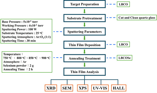
Figure 1.
The experimental procedure for LaCuOSe:Ba.
First, high-purity powders of lanthanum oxide (La2O3), cuprous oxide (Cu2O), and barium carbonate (BaCO3) were weighed and mixed according to the desired stoichiometric ratio corresponding to a 10 atomic percent (at%) barium doping level. The mixture was thoroughly ground and homogenized, followed by high-temperature sintering at 980 °C for 12 h in air to form a dense ceramic target of 10 at% Ba-doped LaCuO2 (LBCO). This target was used for subsequent film deposition.
Second, LBCO thin films were deposited onto quartz glass substrates using radio frequency (RF) magnetron sputtering. The substrates were maintained at room temperature during the deposition process. A reactive sputtering atmosphere consisting of argon and oxygen gases (flow ratio 1:1, total flow rate 20 sccm) was introduced into the sputtering chamber, and the working pressure was kept constant at 4 × 10⁻³ Torr. The deposition time was set to 30 min, resulting in uniform as-deposited films of LBCO composition.
Following deposition, the as-deposited precursor films were transferred into a high-temperature quartz tube furnace for selenization. Approximately 2 g of high-purity selenium powder were placed upstream in the tube, and the entire system was filled with argon gas and sealed at atmospheric pressure (1 atm) to provide an inert and protective environment during annealing. Selenization was conducted at annealing temperatures of 750 °C, 800 °C, 850 °C, and 900 °C for 2 h, enabling the conversion of LBCO as-deposited films into Ba-doped LaCuOSe (LBCOSe) thin films.
The selenization temperature was systematically investigated to explore its influence on the crystallographic structure, phase composition, and optoelectronic properties of the resulting LBCOSe thin films, thereby determining the optimal conditions for achieving high-quality p-type transparent conductive materials.
Next, the crystal structure of the LBCOSe thin films was examined using Glancing Incidence Angle X-ray Diffraction (GIXRD, PANalytical X’PERT PRO, Panalytical, Almelo, The Netherlands) with Cu Kα (λ = 1.5406 Å), operated at 45 kV and 20 mA. To further investigate the microstructural features, the surface and cross-sectional morphologies were observed using field-emission scanning electron microscopy (FE-SEM, Hitachi-4700, Hitachi, Tokyo, Japan). In addition, the chemical composition and bonding states of the films were analyzed via X-ray photoelectron spectroscopy (XPS, JEOL JAMP-9500F Auger Electron Spectroscopy, Akishima, Japan).
During the XPS analysis, surface charging effects may occur. In the spectra, an adventitious carbon (AdC) C 1s peak was detected; however, calibration based on the C 1s peak is not reliable. Therefore, we adopted an alternative approach by calibrating the C 1s binding energy (BE) using the sample work function (ΦSA), according to the relation BE = 289.58 − ΦSA [21,22]. The calculated energy shift was then applied to all core levels. We calibrated using the work function (∼6.0 eV) of divalent ion–doped LaCuOSe thin films reported in [23].
After establishing the structural and compositional characteristics, the electrical properties of the films, including resistivity, carrier mobility, and carrier concentration, were measured using a Hall effect system. Complementary optical characterization was performed by measuring the optical transmittance with a UV–Visible spectrophotometer (Thermo Scientific Evolution 201, Thermo Scientific, USA).
The optical bandgap (Eg) was then determined based on the absorption edge relation (Equation (1) [24]) and the dependence of the absorption coefficient (α) on Eg (Equation (2) [24]).
where n is the transition type parameter (0.5 for direct allowed transition; 2 for indirect allowed transition), α is the absorption coefficient (constant), h is the Planck constant, and ν is the frequency.
The absorption coefficient was obtained from the UV–Vis transmittance data using Equation (3) [24]. Since the reflectance (R) was not measured, a simplified form of Equation (4) [25] was employed. By applying n = 0.5, Tauc plots of (αhν)2 versus photon energy (hν) were constructed. Finally, the optical bandgap was estimated by extrapolating the linear portion of the Tauc plot to the intercept at (αhν)2 = 0, yielding the corresponding Eg value.
where T is the transition type parameter (0.5 for direct allowed transition; 2 for indirect allowed transition), α is the absorption coefficient (constant), h is the Planck constant, and ν is the frequency.
3. Results and Discussion
3.1. Crystal Structure Analysis
Figure 2 presents the X-ray diffraction (XRD) patterns of 10 at% Ba-doped lanthanum copper oxide thin films subjected to selenization annealing at various temperatures (750 °C, 800 °C, 850 °C, and 900 °C). Phase identification was performed using the International Centre for Diffraction Data (ICDD) database. The diffraction peaks observed in samples annealed at 750 °C and 800 °C closely match those of lanthanum copper oxyselenide (LaCuOSe, PDF#49-1221), indicating successful phase formation under these conditions.
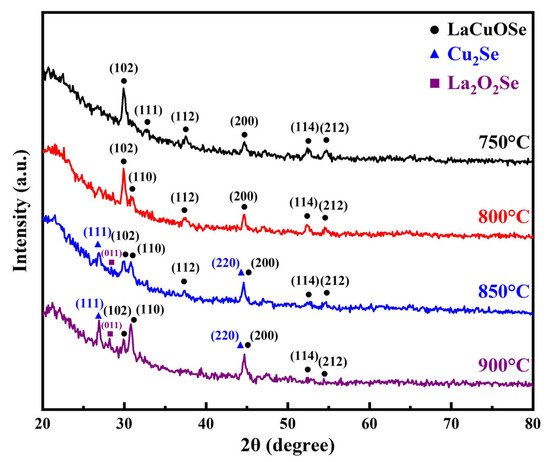
Figure 2.
X-ray diffraction (XRD) patterns of 10 at% Ba-doped lanthanum copper oxide thin films selenized at 750 °C, 800 °C, 850 °C, and 900 °C.
However, at higher annealing temperatures of 850 °C and 900 °C, significant changes in the XRD patterns were observed. Specifically, the most intense diffraction peak shifted from the (102) to the (200) and (110) plane, suggesting a change in preferred crystallographic orientation. Moreover, additional peaks appeared, corresponding to secondary phases identified as copper selenide (Cu2Se, PDF#65-2982) and lanthanum oxyselenide (La2O2Se, PDF#74-0346). These results imply partial decomposition or phase segregation at elevated temperatures. According to the JCPDS card data of LaCuOSe (PDF#49-1221) and Cu2Se (PDF#65-2982), the (110) and (200) planes of LaCuOSe exhibit interplanar spacings close to those of the (200) and (220) planes of Cu2Se. During the crystal growth process, elevated temperatures may facilitate preferential orientation, while the formation of secondary phases at high temperatures is likely to alter the properties of the films.
Similar thermal instability has been reported in other oxychalcogenide systems. For instance, LaCuOS is known to exhibit a complex layered structure and readily decomposes at high temperatures into La2O3, La2O2S, and Cu2S [26]. In a related study, the formation of La2O2S was attributed to copper deficiency during LaCuOS thin film synthesis [27]. The formation of Cu2Se and La2O2Se in our study is likely due to excess Se reacting with La2O3 and Cu2O in the film, following the reaction
2Cu2O(s) + 2La2O3(s) + 5Se(s) → 2LaCuOSe(s) + Cu2Se(s) + La2O2Se(s) + SeO2(g)
Equation (5) is stoichiometrically balanced and reflects experimentally observed secondary phases under Se-rich, oxidizing conditions. The reaction’s thermodynamic driving force principally derives from the formation and volatilization of gaseous SeO2. Literature on LaCuOSe and analogous oxychalcogenides supports the overall reaction pathway and impurity phase evolution.
Table 1 summarizes the XRD results, including diffraction angles (2θ) of the (102) plane, relative intensities, and full width at half maximum (FWHM) values. Interplanar spacings (d-spacings) were calculated using Bragg’s law (nλ = 2dsinθ) [28], and crystallite sizes were estimated using Scherrer’s formula [29]:
where t is the average crystallite size, K is the shape factor (typically 0.9), λ is the X-ray wavelength, β is the FWHM in radians, and θ is the Bragg angle.

Table 1.
A summary of structural parameters obtained via XRD analysis of 10 at% Ba-doped lanthanum copper oxide thin films annealed at different selenization temperatures.
The calculated average grain sizes of the LBCOSe thin films increased slightly with annealing temperature, measured as 37.0 nm at 750 °C, 37.5 nm at 800 °C, 38.1 nm at 850 °C, and 39.3 nm at 900 °C. This trend suggests moderate grain growth facilitated by increased thermal energy.
Lattice parameters were further extracted using Cohen’s method [30], and the results reveal a systematic variation with annealing temperature. As shown in Table 1, the a-axis lattice constant increased from 4.0534 Å to 4.0758 Å, while the c-axis lattice constant decreased from 8.7969 Å to 8.7154 Å as the selenization temperature increased from 750 °C to 900 °C. According to previous literature [31], bond lengths such as Cu–Ch (chalcogen) and Cu–Cu distances are primarily influenced by changes in the a-axis. Therefore, the observed expansion along the a-axis likely modifies the internal bonding geometry within the Cu–Ch layers, potentially influencing both the electrical and optical properties of the films.
These findings demonstrate that while higher annealing temperatures may improve crystallinity and grain size, they also risk introducing undesirable secondary phases that can degrade the optoelectronic performance of the films. Consequently, controlling the selenization temperature is critical for optimizing both the structural and functional properties of LBCOSe thin films.
3.2. Surface Morphology Analysis
Figure 3 displays the surface and cross-sectional scanning electron microscopy (SEM) images of LBCOSe thin films subjected to selenization annealing at various temperatures: (a) 750 °C, (b) 800 °C, (c) 850 °C, and (d) 900 °C. At annealing temperatures of 750 °C and 800 °C, the film surfaces are characterized by uniformly distributed, rounded granular structures, suggesting limited grain growth and nucleation-dominated morphology.
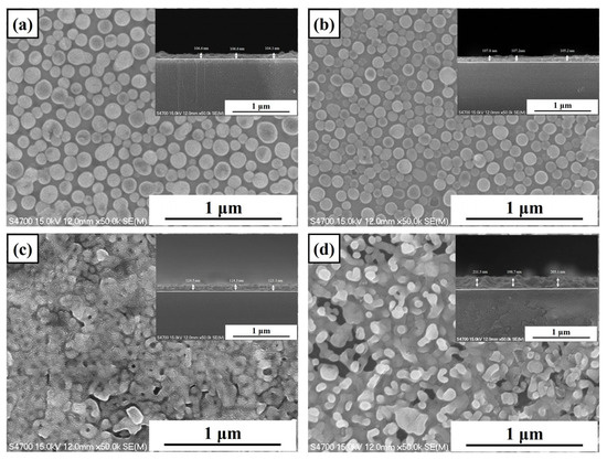
Figure 3.
Surface and cross-sectional scanning electron microscopy (SEM) images of LBCOSe thin films annealed at various selenization temperatures: (a) 750 °C, (b) 800 °C, (c) 850 °C, and (d) 900 °C.
As the annealing temperature increases to 850 °C, distinct signs of grain coalescence become evident, with larger grains beginning to emerge and intergrain boundaries becoming less prominent. At 900 °C, the surface morphology shows significantly enlarged and well-connected grains, indicating enhanced atomic mobility and pronounced grain growth.
Figure 4 displays the grain size distribution curves of LBCOSe thin films annealed at different selenization temperatures: (a) 750 °C, (b) 800 °C, (c) 850 °C, and (d) 900 °C. The average grain size increases from 0.147 µm at 750 °C to 0.289 µm at 900 °C. This trend reflects the enhanced grain coalescence at higher temperatures, accompanied by a decrease in the number of grains, as smaller grains merge to form larger ones.
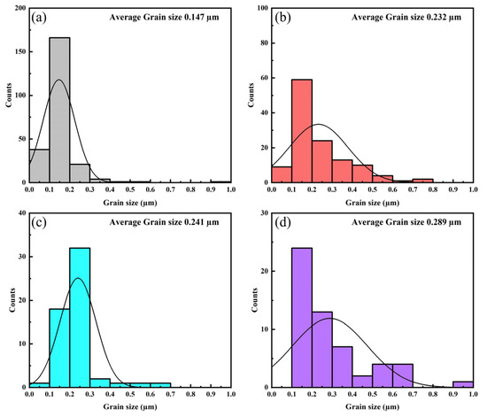
Figure 4.
Grain size distribution curve of LBCOSe thin films annealed at various selenization temperatures: (a) 750 °C, (b) 800 °C, (c) 850 °C, and (d) 900 °C.
The cross-sectional average film thicknesses were 106 nm, 107 nm, 123 nm, and 205 nm, as shown in Figure 3 (a) 750 °C, (b) 800 °C, (c) 850 °C, and (d) 900 °C, respectively. Cross-sectional SEM images further reveal a progressive increase in film thickness with increasing annealing temperature. This increase in thickness is attributed to accelerated grain growth and crystallization kinetics under higher thermal energy conditions during the selenization process. The simultaneous grain coarsening and thickening of the films confirm that elevated annealing temperatures facilitate both lateral and vertical grain expansion, which may directly influence the electrical and optical performance of the resulting thin films.
3.3. X-Ray Photoelectron Spectroscopy (XPS) Analysis
X-ray photoelectron spectroscopy (XPS) was employed to investigate the chemical states and elemental compositions of LBCOSe thin films annealed at different selenization temperatures (750 °C, 800 °C, 850 °C, and 900 °C).
Figure 5 shows the Survey Spectra of LBCOSe thin films annealed at different selenization temperatures: (a) 750 °C, (b) 800 °C, (c) 850 °C, and (d) 900 °C. The spectra reveal characteristic peaks of La 3d (La 3d5/2 and La 3d3/2), O 1s, Cu 2p3/2, Se 3p, and Ba 3d. In addition, a C 1s peak is observed, which is likely attributed to the adsorption of carbon-containing compounds. The binding energies of these peaks are consistent with those reported in the literature [32,33]. The survey and core-level spectra confirmed the presence of La, Cu, O, Se, and Ba in all samples.
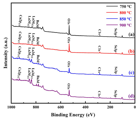
Figure 5.
Survey Spectra of LBCOSe thin films annealed at various selenization temperatures: (a) 750 °C, (b) 800 °C, (c) 850 °C, and (d) 900 °C.
Figure 6 displays the La 3d spectra of LBCOSe thin films annealed at various selenization temperatures: (a) 750 °C, (b) 800 °C, (c) 850 °C, and (d) 900 °C. The binding energy (BE) of La 3d5/2 was observed at 833.94 eV, 834.05 eV, 834.06eV, and 834.02 eV for the samples annealed at 750 °C, 800 °C, 850 °C, and 900 °C, respectively. A characteristic satellite peak appeared at higher binding energies: 837.61 eV, 837.84 eV, 837.82eV, and 837.83 eV, respectively. These values are consistent with previous reports, where the La 3d5/2 binding energy of La in LaCuOSe is approximately 834.3 eV, which is higher than that in La2O3 (831.9 eV) [32]. The satellite peaks located ~4 eV above the main La 3d5/2 peak are attributed to shake-up processes caused by ligand–metal bonding interactions [32,34].
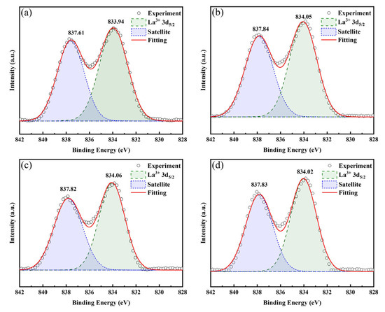
Figure 6.
La 3d spectra of LBCOSe thin films annealed at various selenization temperatures: (a) 750 °C, (b) 800 °C, (c) 850 °C, and (d) 900 °C.
Figure 7 displays the O 1s spectra of LBCOSe thin films annealed at various selenization temperatures: (a) 750 °C, (b) 800 °C, (c) 850 °C, and (d) 900 °C, respectively. Three distinct peaks were identified in all samples. The first peak appears at ~529 eV (528.66, 528.85, 528.84, and 528.93 eV), the second at ~530 eV (530.09, 530.12, 530.05, and 530.35 eV), and the third at ~531 eV (531.53, 531.28, 531.15, and 531.49 eV). These peak positions differ from those reported in Ref. [32]. According to Ref. [35], by analogy, it is inferred that in Ba-doped LaCuOSe, the peak around 529.0 eV corresponds to lattice oxygen, the peak near 530.0 eV is characteristic of OH groups adsorbed on the oxide surface, and the peak at ~531 eV originates from surface oxygen species.
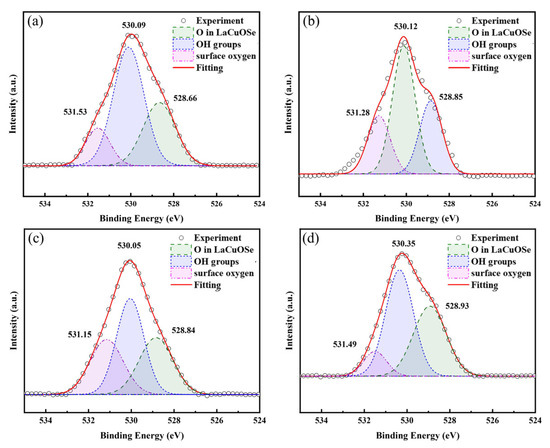
Figure 7.
O 1s spectra of LBCOSe thin films annealed at various selenization temperatures: (a) 750 °C, (b) 800 °C, (c) 850 °C, and (d) 900 °C.
Figure 8 displays the Cu 2p3/2 spectra of LBCOSe thin films annealed at various selenization temperatures: (a) 750 °C, (b) 800 °C, (c) 850 °C, and (d) 900 °C, which show the Cu 2p3/2 peaks for the four selenization temperatures. The observed binding energies are 931.95 eV, 932.31 eV, 932.82 eV, and 932.36 eV, respectively. These values are consistent with the Cu+ oxidation state, whose typical 2p3/2 peak lies between 932.7 and 932.9 eV, and do not align with Cu2+ species, which exhibit peaks above 933.5 eV [32].
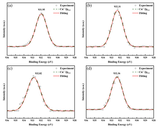
Figure 8.
Cu 2p3/2 spectra of LBCOSe thin films annealed at various selenization temperatures: (a) 750 °C, (b) 800 °C, (c) 850 °C, and (d) 900 °C.
Figure 9 displays the Ba 3d spectra of LBCOSe thin films annealed at various selenization temperatures: (a) 750 °C, (b) 800 °C, (c) 850 °C, and (d) 900 °C. In samples annealed at 750 °C, 800 °C, 850 °C, and 900 °C, two distinct Ba 3d peaks are observed—the first at 780.49 eV, 779.84 eV, 778.81 eV, and 777.36 eV, and the second at 781.96 eV, 781.30 eV, 779.74 eV, and 779.76 eV, respectively. This may be due to insufficient Ba substitutions at La sites, as reported in [36], which indicates that a well-defined Ba 3d spectrum becomes evident only when Ba substitution at the La site exceeds 10 mol%. The observed binding energy peaks are close to the Ba 3d5/2 binding energy of Ba-O (779.9 eV) reported in Ref. [33], suggesting that Ba substitutes for La and bonds with O.
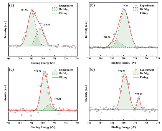
Figure 9.
Ba 3d spectra of LBCOSe thin films annealed at various selenization temperatures: (a) 750 °C, (b) 800 °C, (c) 850 °C, and (d) 900 °C.
Figure 10 displays the Se 3d spectra of LBCOSe thin films annealed at various selenization temperatures: (a) 750 °C, (b) 800 °C, (c) 850 °C, and (d) 900 °C. Each sample displays two distinct peaks. The first peak appears at 53.39 eV, 53.41 eV, 53.70 eV, and 53.61 eV, and the second appears at 54.36 eV, 54.43 eV, 54.54 eV, and 54.70 eV for the four annealing temperatures, respectively, which is consistent with the reported values for LaCuOSe in Ref. [37] and can be split into the Se 3d5/2 and Se 3d3/2 orbitals, respectively.
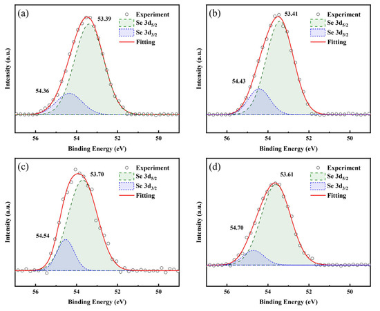
Figure 10.
Se 3d spectra of LBCOSe thin films annealed at various selenization temperatures: (a) 750 °C, (b) 800 °C, (c) 850 °C, and (d) 900 °C.
3.4. Optical Properties
Figure 11 illustrates the optical transmittance spectra and corresponding Tauc plots for LBCOSe thin films annealed at different selenization temperatures (750 °C, 800 °C, 850 °C, and 900 °C). At 750 °C and 800 °C, the films exhibit the average visible light transmittance values of approximately 65% and 59%, respectively. These values are in close agreement with the ~50% transmittance reported for Mg-doped LaCuOSe films in the literature [15]. The arrows in the inset figure mark the band gap position. The estimated optical bandgaps for these samples are 3.17 eV and 3.12 eV, respectively, aligning well with previously reported values for LaCuOSe (2.9 and 3.1 eV) [38].
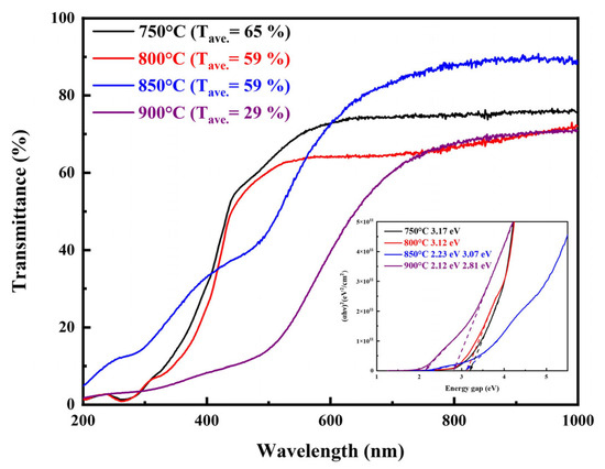
Figure 11.
Optical transmittance spectra and Tauc plots of LBCOSe thin films annealed at different selenization temperatures (750 °C, 800 °C, 850 °C, and 900 °C).
At higher annealing temperatures (850 °C and 900 °C), the optical properties undergo significant changes. The average transmittance drops to 59% and 29%, respectively, which correlates with the formation of secondary phases such as Cu2Se, as confirmed by XRD and XPS analyses. Notably, the optical absorption edges for these samples reveal two distinct bandgap regions. The higher bandgaps of near 3.07 eV for the 850 °C sample were 2.81 eV for the 900 °C sample, which are within the expected range for LaCuOSe [38], but the slight redshift suggests increasing disorder or defect-related absorption.
A sharp decline in transmittance near 400 nm is observed across all LaCuOSe samples. This behavior aligns with previous reports on LaCuOS, where the presence of copper vacancies was shown to introduce localized electronic states within the bandgap, thereby enhancing sub-bandgap absorption and reducing optical transparency in this spectral region [27]. The pronounced drop in transmittance near 400 nm thus reflects the onset of strong absorption associated with intrinsic defect states, particularly in Cu-deficient compositions.
The lower bandgaps of near 2.23 eV for the 850 °C sample and 2.12 eV for the 900 °C sample correspond closely to the direct bandgap of Cu2Se, which typically ranges from 2.0 to 2.4 eV [39]. This secondary absorption feature indicates that as the annealing temperature increases, the contribution of Cu2Se to the overall optical response becomes more significant. Furthermore, prior studies have shown that Cu2Se thin films exhibit reduced transmittance and narrower bandgaps at higher annealing temperatures due to densification and increased carrier concentration [40].
Overall, these findings demonstrate that while moderate annealing temperatures can preserve high optical transparency and desirable bandgap characteristics in Ba-doped LaCuOSe thin films, excessive thermal treatment leads to phase separation and optical degradation due to the formation of Cu2Se.
3.5. Electrical Property Analysis
Figure 12 presents the Hall effect measurement results for LBCOSe thin films annealed at selenization temperatures of 750 °C, 800 °C, 850 °C, and 900 °C. There is a clear correlation between increasing selenization temperature and electrical performance: as the temperature rises, the carrier concentration increases markedly, resulting in a significant decrease in electrical resistivity.
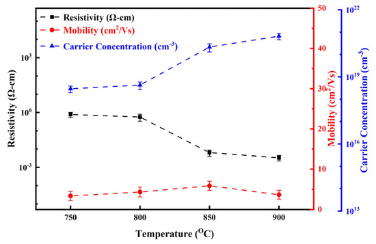
Figure 12.
Hall effect measurements of LBCOSe thin films annealed at different selenization temperatures (750 °C, 800 °C, 850 °C, and 900 °C).
At 850 °C and 900 °C, both carrier concentration and conductivity improve sharply, while resistivity drops significantly. These abrupt changes are consistent with the formation of the Cu2Se secondary phase, which is known for its high intrinsic conductivity. Compared to values in the literature, Mg-doped LaCuOSe films typically exhibit a carrier concentration of approximately 2 × 1020 cm−3 with a maximum conductivity of 140 S·cm−1 [15]. In contrast, Cu2Se films have been reported to have significantly higher carrier concentrations ranging from 4 × 10²⁰ to 5 × 1021 cm−3 and a minimum resistivity of 3.94 × 10⁻⁴ Ω·cm [41]. These findings strongly suggest that the enhanced electrical performance observed in the high-temperature samples is caused by the increasing contribution of the Cu2Se phase.
3.6. Optoelectronic Figure of Merit (FOM) Analysis
Figure 13 presents the optoelectronic figure of merit (FOM) for LBCOSe thin films annealed at various selenization temperatures (750 °C, 800 °C, 850 °C, and 900 °C). The FOM was calculated using the Haacke equation [42], which is widely adopted to evaluate the overall optoelectronic performance of transparent conductive materials:
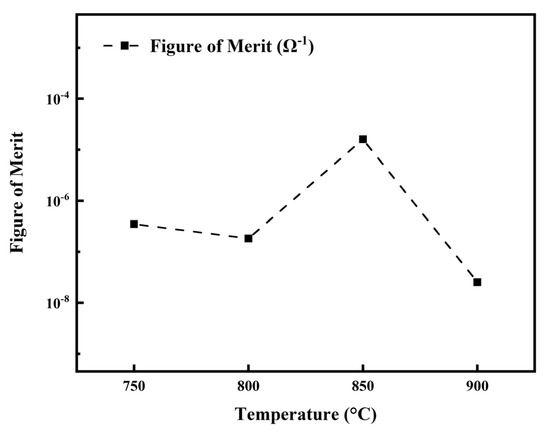
Figure 13.
Optoelectronic figure of merit (FOM) of LBCOSe thin films annealed at different selenization temperatures.
(φTC = figure of merit, T = optical transmission (%), RS = electrical sheet resistance (Ω)).
While the film annealed at 750 °C exhibited the highest visible light transmittance (65%), its relatively high resistivity (7.72 × 10⁻¹ Ω·cm) significantly reduced FOM. In contrast, the film annealed at 900 °C showed the lowest resistivity (3.33 × 10⁻³ Ω·cm), but its poor transmittance (29%) led to a similarly low FOM. These results underscore the importance of balancing optical and electrical properties.
The film annealed at 850 °C demonstrated the most favorable balance, with a moderate transmittance of 59% and a low resistivity of 6.37 × 10⁻³ Ω·cm. As a result, it achieved the highest FOM (1.6 × 10⁻⁵ Ω−1) among all samples, indicating that 850 °C is the optimal selenization temperature for enhancing the overall optoelectronic performance of Ba-doped LaCuOSe thin films. Table 2 summarizes a comparison between LBCOSe and other reported LaCuOSe studies. The results indicate that, under different selenization annealing temperatures, Ba-doped LaCuOSe thin films exhibit an increased bandgap and enhanced transmittance. Furthermore, the presence of an appropriate amount of Cu2Se markedly improves the electrical properties of the films. In contrast, excessively high selenization annealing temperatures result in a reduction in transmittance in the LBCOSe thin films.
Table 2.
Summary of a comparison between LBCOSe and other reported LaCuOSe studies.
4. Conclusions
XRD and XPS analyses confirmed that the main phase in all LBCOSe thin films was LaCuOSe. However, when the selenization annealing temperature exceeded 850 °C, secondary phases such as Cu2Se and La2O2Se were detected, likely due to thermal decomposition of the LaCuOSe lattice at high temperatures.
The optical transmittance of the films decreased progressively with increasing selenization temperature, accompanied by a corresponding reduction in optical bandgap. This trend is particularly evident above 850 °C, where the formation of Cu2Se introduces additional sub-bandgap absorption. At 900 °C, the transmittance dropped sharply, which can be attributed not only to the emergence of Cu2Se but also to increased film thickness, as observed in SEM cross-sectional images.
Electrically, films annealed above 850 °C exhibited a marked increase in carrier concentration and a significant drop in resistivity, again attributed to the conductive nature of the Cu2Se phase.
Among all tested conditions, the film annealed at 850 °C demonstrated the best overall optoelectronic performance. It achieved an average visible transmittance of 59%, a low resistivity of 6.37 × 10⁻³ Ω·cm, a carrier mobility of 5.87 cm2/V·s, and a high carrier concentration of 2.15 × 1020 cm−3. These combined properties resulted in the highest figure of merit (FOM) of 1.6 × 10⁻⁵ Ω−1.
In conclusion, selenization at 850 °C offers the optimal balance between phase purity, optical transparency, and electrical conductivity, making it the most favorable condition for fabricating high-performance Ba-doped LaCuOSe thin films for transparent optoelectronic applications.
Author Contributions
C.-Y.H. contributed to the conception and design of experiments and to writing the manuscript. G.-J.C. supervised the analysis and edited the manuscript. G.-Y.W., C.-N.W. and P.-S.C. provided technical support and conceptual advice. G.-J.C. contributed extensively to the work as the corresponding author. All authors have read and agreed to the published version of the manuscript.
Funding
This research was funded by NSTC grant number NSTC113-2813-C-214-014-E.
Conflicts of Interest
The authors declare no conflicts of interest.
References
- Ginley, D.S.; Perkins, J.D. Transparent conductors. In Handbook of Transparent Conductors; Springer: Berlin/Heidelberg, Germany, 2010; pp. 1–25. [Google Scholar]
- Balaprakash, V.; Thangavel, K.; Mohan, M.; Gowrisankar, P.; Sakthivel, R. Thin Film Transparent Conducting Oxides and its Anticorrosion and Surface Protection Applications: A Review. In Novel Anti-Corrosion and Anti-Fouling Coatings and Thin Films; Scrivener Publishing LLC.: Beverly, MA, USA, 2024; pp. 109–127. [Google Scholar]
- Guillen, C.; Herrero, J. TCO/metal/TCO structures for energy and flexible electronics. Thin Solid Films 2011, 520, 1–17. [Google Scholar] [CrossRef]
- Zhao, Y.; Dong, W.; Fang, X.; Zhou, Y.; Meng, G.; Tao, R.; Deng, Z.; Zhou, S.; Dai, S. P-type Ca doped SrCu2O2 thin film: Synthesis, optical property and photovoltaic application. J. Alloys Compd. 2012, 513, 50–54. [Google Scholar] [CrossRef]
- Ginley, D.S.; Bright, C. Transparent conducting oxides. MRS Bull. 2000, 25, 15–18. [Google Scholar] [CrossRef]
- Habis, C.; Zaraket, J.; Aillerie, M. Transparent conductive oxides. Part I. general review of structural, electrical and optical properties of TCOs related to the growth techniques, materials and dopants. Defect Diffus. Forum 2022, 417, 243–256. [Google Scholar] [CrossRef]
- Chey, S.J.; Liu, W.; Yuan, M.; Mitzi, D.B. Characterization of indium tin oxide and al-doped Zinc oxide thin films deposited by confocal RF magnetron sputter deposition. In Proceedings of the 2009 34th IEEE Photovoltaic Specialists Conference (PVSC), Philadelphia, PA, USA, 7–12 June 2009; pp. 001149–001153. [Google Scholar]
- Singh, J.; Bhardwaj, P.; Kumar, R.; Verma, V. Progress in developing highly efficient p-Type TCOs for transparent electronics: A comprehensive review. J. Electron. Mater. 2024, 53, 7179–7210. [Google Scholar] [CrossRef]
- Tripathi, T.S.; Karppinen, M. Atomic layer deposition of p-type semiconducting thin films: A review. Adv. Mater. Interfaces 2017, 4, 1700300. [Google Scholar] [CrossRef]
- Yin, Y.; Wu, Y.; Chen, G.; Yin, W.-J. Double perovskite Ba2BiTaO6 as a promising p-type transparent conductive oxide: A first-principles defect study. J. Appl. Phys. 2020, 127, 175703. [Google Scholar] [CrossRef]
- Kawazoe, H.; Yasukawa, M.; Hyodo, H.; Kurita, M.; Yanagi, H.; Hosono, H. P-type electrical conduction in transparent thin films of CuAlO2. Nature 1997, 389, 939–942. [Google Scholar] [CrossRef]
- Palazzi, M. Préparation et affinement de la structure de (LaO) CuS. C. R. Acad. Sci. 1981, 292, 7899–7919. [Google Scholar]
- Ueda, K.; Inoue, S.; Hirose, S.; Kawazoe, H.; Hosono, H. Transparent p-type semiconductor: LaCuOS layered oxysulfide. Appl. Phys. Lett. 2000, 77, 2701–2703. [Google Scholar] [CrossRef]
- Ueda, K.; Hosono, H. Crystal structure of LaCuOS1−xSex oxychalcogenides. Thin Solid Films 2002, 411, 115–118. [Google Scholar] [CrossRef]
- Hiramatsu, H.; Ueda, K.; Ohta, H.; Hirano, M.; Kamiya, T.; Hosono, H. Wide gap p-type degenerate semiconductor: Mg-doped LaCuOSe. Thin Solid Films 2003, 445, 304–308. [Google Scholar] [CrossRef]
- Hiramatsu, H.; Kamioka, H.; Ueda, K.; Hirano, M.; Hosono, H. Electrical and photonic functions originating from low-dimensional structures in wide-gap semiconductors LnCuOCh (Ln = lanthanide, Ch = chalcogen): A review. J. Ceram. Soc. Jpn. 2005, 113, 10–16. [Google Scholar] [CrossRef][Green Version]
- Ueda, K.; Hiramatsu, H.; Ohta, H.; Hirano, M.; Kamiya, T.; Hosono, H. Single-atomic-layered quantum wells built in wide-gap semiconductors Ln CuO Ch (Ln = lanthanide, Ch = chalcogen). Phys. Rev. B 2004, 69, 155305. [Google Scholar] [CrossRef]
- Zhang, N.; Gong, H. P-type transparent LaCuOS semiconductor synthesized via a novel two-step solid state reaction and sulfurization process. Ceram. Int. 2017, 43, 6295–6302. [Google Scholar] [CrossRef]
- Ha, C.; Chung, Y.J. Thin films as practical quantum materials: A status quo and beyond. APL Mater. 2024, 12, 120901. [Google Scholar] [CrossRef]
- Sakthinathan, S.; Meenakshi, G.A.; Vinothini, S.; Yu, C.-L.; Chen, C.-L.; Chiu, T.-W.; Vittayakorn, N. A review of thin-film growth, properties, applications, and future prospects. Processes 2025, 13, 587. [Google Scholar] [CrossRef]
- Greczynski, G.; Hultman, L. A step-by-step guide to perform x-ray photoelectron spectroscopy. J. Appl. Phys. 2022, 132, 011101. [Google Scholar] [CrossRef]
- Yakushova, N.D.; Gubich, I.A.; Karmanov, A.A.; Komolov, A.S.; Koroleva, A.V.; Korotcenkov, G.; Pronin, I.A. Photocatalytic Degradation of Toxic Dyes on Cu and Al Co-Doped ZnO Nanostructured Films: A Comparative Study. Technologies 2025, 13, 277. [Google Scholar] [CrossRef]
- Yanagi, H.; Kikuchi, M.; Kim, K.-B.; Hiramatsu, H.; Kamiya, T.; Hirano, M.; Hosono, H. Low and small resistance hole-injection barrier for NPB realized by wide-gap p-type degenerate semiconductor, LaCuOSe: Mg. Org. Electron. 2008, 9, 890–894. [Google Scholar] [CrossRef]
- Ong, C.H.; Gong, H. Effects of aluminum on the properties of p-type Cu–Al–O transparent oxide semiconductor prepared by reactive co-sputtering. Thin Solid Films 2003, 445, 299–303. [Google Scholar] [CrossRef]
- Hartnagel, H. Semiconducting Transparent Thin Films; CRC Press: Boca Raton, FL, USA, 1995. [Google Scholar]
- Hiramatsu, H.; Ueda, K.; Ohta, H.; Orita, M.; Hirano, M.; Hosono, H. Heteroepitaxial growth of a wide-gap p-type semiconductor, LaCuOS. Appl. Phys. Lett. 2002, 81, 598–600. [Google Scholar] [CrossRef]
- Zhang, N.; Liu, X.; Annadi, A.; Tang, B.; Gong, H. Highly conducting p-type transparent LnCuOS (Ln= La and Nd) and p–n junction by using ink. ACS Appl. Electron. Mater. 2019, 1, 1605–1615. [Google Scholar] [CrossRef]
- Zheng, X.; Li, J.; Zhou, Y. X-ray diffraction measurement of residual stress in PZT thin films prepared by pulsed laser deposition. Acta Mater. 2004, 52, 3313–3322. [Google Scholar] [CrossRef]
- Kulkarni, A.; Schulz, K.H.; Lim, T.; Khan, M. Dependence of the sheet resistance of indium-tin-oxide thin films on grain size and grain orientation determined from X-ray diffraction techniques. Thin Solid Films 1999, 345, 273–277. [Google Scholar] [CrossRef]
- Cullity, B. Elements of X-Ray Diffraction; Addison-Wesley Publishing Co.: New York, NY, USA, 1986. [Google Scholar]
- Ueda, K.; Takafuji, K.; Yanagi, H.; Kamiya, T.; Hosono, H.; Hiramatsu, H.; Hirano, M.; Hamada, N. Optoelectronic properties and electronic structure of YCuOSe. J. Appl. Phys. 2007, 102, 113714. [Google Scholar] [CrossRef]
- Rudyk, B.W.; Blanchard, P.E.; Cavell, R.G.; Mar, A. Electronic structure of lanthanum copper oxychalcogenides LaCuOCh (Ch= S, Se, Te) by X-ray photoelectron and absorption spectroscopy. J. Solid State Chem. 2011, 184, 1649–1654. [Google Scholar] [CrossRef]
- Evangelou, E.; Konofaos, N.; Aslanoglou, X.; Kennou, S.; Thomas, C. Characterization of BaTiO3 thin films on p-Si. Mater. Sci. Semicond. Process. 2001, 4, 305–307. [Google Scholar] [CrossRef]
- Oh, S.-J.; Kim, G.-H.; Sawatzky, G.; Jonkman, H. Effect of hole-induced shakedown in the Auger spectrum of lanthanum. Phys. Rev. B 1988, 37, 6145. [Google Scholar] [CrossRef][Green Version]
- Frankcombe, T.J.; Liu, Y. Interpretation of oxygen 1s X-ray photoelectron spectroscopy of ZnO. Chem. Mater. 2023, 35, 5468–5474. [Google Scholar] [CrossRef]
- Gunasekaran, N.; Rajadurai, S.; Carberry, J.; Bakshi, N.; Alcock, C. Surface characterization and catalytic properties of La1−xAxMO3 perovskite oxides. Part II. Studies on La1−xBaxMnO3 (0 ≤ x ≤ 0.2) oxides. Solid State Ion. 1995, 81, 243–249. [Google Scholar] [CrossRef]
- Rudyk, B.W.; Blanchard, P.E.; Cavell, R.G.; Mar, A. X-ray photoelectron and absorption spectroscopy of mixed lanthanum copper oxychalcogenides LaCuOSe1−xTex (0 ≤ x ≤ 1). J. Alloys Compd. 2012, 514, 199–204. [Google Scholar] [CrossRef]
- Kamioka, H.; Hiramatsu, H.; Hayashi, K.; Hirano, M.; Hosono, H. Photonic materials utilizing naturally occurring nanostructures. J. Photochem. Photobiol. A Chem. 2004, 166, 141–147. [Google Scholar] [CrossRef]
- Rudradawong, C.; Khammuang, S.; Kotmool, K.; Bovornratanaraks, T.; Limsuwan, P.; Somdock, N.; Sakdanuphab, R.; Sakulkalavek, A. Enhanced thermoelectric properties of Cu2Se via Sb doping: An experimental and computational study. J. Eur. Ceram. Soc. 2023, 43, 401–406. [Google Scholar] [CrossRef]
- Ali, S.M.; Hassun, H.; Salih, A.; Athab, R.; Al-Maiyaly, B.; Hussein, B. Study the properties of Cu2Se thin films for optoelectronic applications. Chalcogenide Lett. 2022, 19, 663–671. [Google Scholar] [CrossRef]
- Li, Y.; Gao, X.; Yang, C.; Huang, F. The effects of sputtering power on optical and electrical properties of copper selenide thin films deposited by magnetron sputtering. J. Alloys Compd. 2010, 505, 623–627. [Google Scholar] [CrossRef]
- Haacke, G. New figure of merit for transparent conductors. J. Appl. Phys. 1976, 47, 4086–4089. [Google Scholar] [CrossRef]
Disclaimer/Publisher’s Note: The statements, opinions and data contained in all publications are solely those of the individual author(s) and contributor(s) and not of MDPI and/or the editor(s). MDPI and/or the editor(s) disclaim responsibility for any injury to people or property resulting from any ideas, methods, instructions or products referred to in the content. |
© 2025 by the authors. Licensee MDPI, Basel, Switzerland. This article is an open access article distributed under the terms and conditions of the Creative Commons Attribution (CC BY) license (https://creativecommons.org/licenses/by/4.0/).