Article

Effect of Mid-Frequency and Inductively Coupled Plasma on the Properties of Molybdenum Nitride Thin Films

School of Mechanical and Ocean Engineering, Mokpo National University, Jeonnam 58554, Republic of Korea
Coatings 2025, 15(10), 1155; https://doi.org/10.3390/coatings15101155
Submission received: 3 September 2025 / Revised: 29 September 2025 / Accepted: 30 September 2025 / Published: 3 October 2025
(This article belongs to the Section Thin Films)

Abstract

This study focuses on the characterization of MoN thin films deposited by the direct current magnetron sputtering (dcMS), mid-frequency magnetron sputtering (mfMS), and inductively coupled plasma magnetron sputtering (ICPMS) methods. Two mixed metallic phases, namely, α-Mo and γ-Mo2N, were detected from the film obtained using the dcMS, whereas only single γ-Mo2N phase was detected from the films obtained using the mfMS and ICPMS. Furthermore, the residual stress of the deposited thin films was strongly dependent on the sputtering process. As the mfMS and ICPMS deposition process were introduced, the film morphology changed from a porous columnar to a dense structure with finer grains than film deposited using dcMS. The surface roughness and crystal grain size of coated films were investigated by atomic force microscopy and X-ray diffraction analysis methods. Furthermore, the variation in hardness and electrical resistivity of the MoN thin films deposited by three plasma-enhanced magnetron sputtering was explained on the basis of microstructure and residual stress of the thin films.

1. Introduction

The investigation of transition metal nitrides in the form of thin films is of particular scientific and technological importance. Molybdenum nitride (MoN) is one such material that exhibits interesting properties, α-molybdenum (α-Mo) and MoN have attracted attention due to their electrical, electronic, mechanical, and chemical properties such as superconductivity, high hardness, high melting point, and excellent chemical stability [1,2,3]. Due to these outstanding properties, Mo and MoN thin films are considered the best candidates for wear and corrosion resistant coatings in engineering ceramics [4], diffusion barriers in microelectronics [5], and back contact materials in Cu(In, Ga)Se2 thin film solar cells [6].
Recent studies have attempted to utilize MoN thin films for developing advanced anode materials for lithium-ion batteries and nanosheets for hydrogen storage [7,8]. However, as the properties of MoN thin films may differ considerably from those of bulk MoN materials, further systematic and specific studies are needed. Although there is a already literature on the study of MoN thin films, a detailed analysis of the relationship between the effects of plasma process variables on the electrical and mechanical properties of these films during sputter deposition is still lacking.
To date, cathodic arc, plasma spraying, direct current (DC) sputtering, and chemical vapor deposition methods have been investigated for the fabrication of polycrystalline MoN thin films [9,10,11]. In particular, the mid-frequency sputtering and inductively coupled plasma-assisted magnetron sputtering (ICPMS) have recently gained attention. These methods use pulsed DC or radio frequency antennas capable of generating intermediate frequency or inductively coupled plasma instead of plasma [12]. Our lab has previously reported the applicability of various nitride thin films using mid-frequency magnetron sputtering (mfMS), which solves the problems such as arcing and target poisoning of conventional direct current magnetron sputtering (dcMS) [13,14]. Using such mid-frequency or inductively coupled plasmas, the plasma density can be increased to 1012–1013 cm−3 at process pressures as low a few mTorr. This enables the fabrication of superior thin films with very dense microstructures and the 3D coating of three-dimensional substrates, which is expected to expand the applications of coating technology [15]. In this study, we specifically focused on the effects of plasma-enhanced sputtering on the microstructure, physical crystal structure, mechanical properties, and electrical properties of MoN thin films.

2. Materials and Methods

In this experiment, three types of MoN thin films were prepared by dcMS method using DC power, the mfMS method using pulsed DC power, and the ICPMS method using RF induced inductively coupled plasma (Table 1). A 99.95% pure Mo target with a diameter of 7.6 cm and a thickness of 0.6 cm was used as the starting material. Futhermore, ultrahigh purity Ar and N2 gases were used. Through preliminary experiments, the Ar and N2 gas flow rates were fixed at 20 and 9 sccm, respectively, for the fabrication of thin films with a γ-Mo2N single phase. During deposition, the distance between the substrate and target was kept at 60 mm, and the substrate was rotated at a speed of ~10 rpm to ensure uniform coating. An n-type Si(100) single crystal wafer with a diameter of 10 cm was used as a substrate material. Ultrasonic cleaning was performed in acetone and ethyl alcohol for 10 min each to remove impurities from the substrate surface. Additionally, the targets and substrates were each pretreated with a high-purity Ar plasma for 10 min to remove all impurities adsorbed on the surface. The power used for substrate ion cleaning in this experiment was 10 W (500 V × 0.02 A). The initial pressure in the chamber was evacuated to ap-proximately 1.4 × 10⁻⁴ Torr using a rotary and turbomolecular pumps, while the total pro-cess pressure (Ar + N2) was maintained at 2 mTorr. High-resolution X-ray diffraction (XRD) (Multi-Purpose X-Ray Diffractometer, PANalytical, Almelo, Netherlands) was used to analyze the crystal structure of the obtained MoN thin films, and Field Emission Scanning Electron Microscopy (FE-SEM) (Field-Emission Scanning Electron Microscope, S-3500N, Chiba, Japan) was performed to observe the microstructure of the surface and cross-section of the films. Auto Probe Atomic Force Microscopy (AFM) (Atomic Force Microscopy, Park Systems/Park NX15, Suwon, Korea) was conducted to measure the surface roughness of the thin films. The hardness and elastic modulus of the thin films were measured using an ultraprecise nanoindentation tester nanoindenter (Helmut Fischer, Picodentor HM500, Helmut Fischer, Sindelfingen, Germany). The hardness was averaged over 16 experiments using a Berkovich diamond indenter. The measuring distance of the nanoindenter was kept over 10 μm to avoid any influence from the hard-ness measuring tips that had already performed a measurement. The electrical resistance of the MoN thin films was measured with a Semiconductor Characterization System (SUMMIT (11862B)/4200 SCS, Cascade/Keithley, Beaverton, OR, USA) using the van der Pauw method, which is suita-ble for precise resistance measurements of conductive thin films.

3. Results

3.1. Crystal Structure

The results of X-ray diffraction analysis of MoN thin films prepared by three sputtering methods, i.e., dcMS, mfMS, and ICPMS, are shown in Figure 1. From the XRD results, it can be seen that γ-Mo2N (pdf 25-1366) thin films with face-centered cubic (fcc) structure were prepared in all coated films. In addition to the γ-Mo2N (111), (200), (220), and (311) peaks, an α-Mo (110) peak was observed in the MoN-coated films prepared via dcMS. However, only the γ-Mo2N single phase peak was observed in the MoN-coated films prepared by the mfMS and ICPMS methods.
Meanwhile, it can be seen that the full width at half maximum of the MoN (111) peak prepared by the mfMS and ICPMS methods increases successively compared to the MoN thin film prepared by the dcMS method. The calculation of the average crystallite size using the Scherrer equation based on the (111) peak [16] shows that the average crystallite sizes of the MoN thin films prepared via the dcMS, mfMS, and ICPMS are 10.0, 8.5, and 6.8 nm, respectively; the average crystallite size reduced by up to ~32% for the ICPMS method compared to the dcMS method. A recent study on CrN thin films reported that the ion flux density increases with the generation and introduction of inductively coupled plasma, thereby decreasing the average crystallite grain size and increasing the density of the microstructure of the thin films [17].

3.2. Residual Stress

The residual stress results of the MoN thin films prepared by three sputtering methods, i.e., dcMS, mfMS, and ICPMS methods, are shown in Figure 2. Residual stresses generally affect all properties of thin films, including hardness, electrical resistance, adhesion, and wear and fatigue resistance.
Furthermore, residual stresses (compressive and tensile stresses) in thin films lead to an upshift or downshift of the 2θ value of the MoN X-ray diffraction peak in the stress-free state. The residual stress in the deposited thin film is closely related to the lattice strain caused by intense sputtering, heating of the deposition layer by high-energy ions, point formation defects (void formation due to the bombardment effect of high-energy ions), and lattice distortions (strain). In general, stresses due to lattice distortions cause compressive stresses [18].
In this study, the residual stress was calculated by substituting the 2θ value of the γ-Mo2N (111) peak, which is the main crystal plane, into Equations (1)–(3). Specific values are shown in Table 2.
d = nλ/2sinθ
∆d/d = [d (measured value) − d (ICSD)]/d (ICSD)
Residual stress = ∆d/d × elastic modulus
Figure 2 shows the residual stresses of MoN thin films prepared by the dcMS, mfMS, and ICPMS methods. The obtained residual stresses are 1.98 GPa (dcMS), 0.78 GPa (mfMS), and −7.9 GPa (ICPMS), which shows that the residual stress values change substantially depending on the preparation method of the thin film. In particular, the residual stress values of γ-Mo2N thin films prepared by the ICPMS method were reduced by up to 9.88 GPa compared to those prepared by the dcMS method. This result indicates that the residual stress in the thin film produced by the dcMS method is converted to tensile stress, whereas the residual stress in the thin film produced by the ICPMS method is converted to compressive stress.
EerNisse [19,20] has shown that the residual stress in MoN thin films prepared using a plasma focus device can change from tensile to compressive stress. These induced residual stresses are closely related to the collision of high-energy ions during the formation of the thin film.
It is assumed that the increase in plasma density and the collisions of the high-energy ions with the substrate during the film formation process using the mfMS and ICPMS methods have a considerable impact on the increase in compressive stress in the prepared thin films. It is expected that the increase in compressive stress by this method of thin film preparation has a significant impact on the final crystallite refinement and the increase in mechanical hardness, which is discussed in the following Figure 3 and Figure 4.

3.3. Microstructure

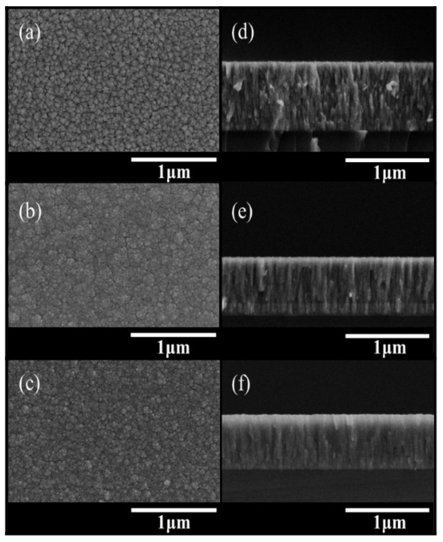
The microstructures of the MoN thin films prepared using three sputtering methods, i.e., dcMS, mfMS, and ICPMS methods, were observed using FE-SEM. Figure 3 shows the surface and cross-sectional images of each film. The surface images of the MoN thin films shows the thin films prepared by the mfMS and ICPMS methods have a small, round granular morphology, a uniform particle size distribution, and a high density compared to those prepared by the dcMS method.
Alternatively, the thin film prepared by the dcMS method has a sharp, wedge-faceted polyhedron morphology, and several inter-granular voids are present between the wedge-shaped polyhedron particles. Moreover, a comparison of the cross-sectional images of the MoN thin films shows that the MoN thin films prepared by ICPMS have a dense microstructure with almost no interparticle space, i.e., no voids. However, crystallites with a columnar structure with distinct interfaces between the particles can be observed in the MoN thin films prepared by the dcMS method.
A non-contact AFM analysis was performed to investigate the effects of the three fabrication methods, i.e., dcMS, mfMS, and ICPMS methods, on the average surface roughness (Ra) of the MoN thin films. The results show that there is a close correlation between the sputtering deposition process and the surface roughness of the thin films. The surface roughness of the thin films prepared by the dcMS, mfMS, and ICPMS methods is 3.2, 2.8, and 2.6 nm, respectively; the surface roughness of the thin films deposited by the ICPMS method is 19% less than that prepared using the dcMS method. It is suggested that the generation of highly ionized plasma using the mfMS and ICPMS methods increased the opportunity to effectively enhance their adatom mobility even after reaching the substrate surface, resulting in a flattening of the thin film surface. In addition, higher ionization fraction of the deposition flux leads to smoother surfaces by mechanisms such as, decreasing clustering in the vapor phase and bicollision of high energy ions at the film surface.

3.4. Nanoindentation Hardness and Elastic Modulus

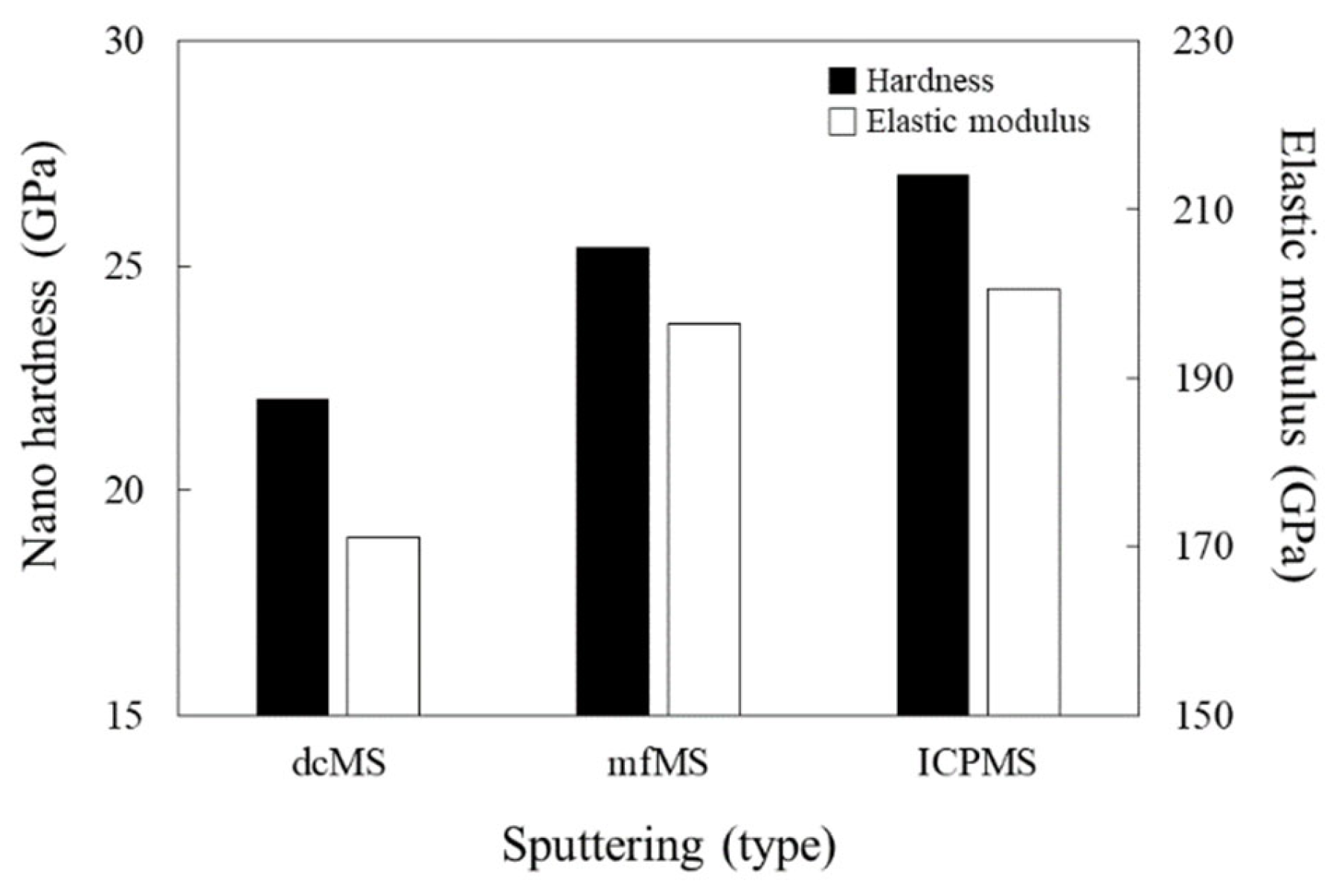
An ultraprecise nanoindentation tester was used to measure the nanohardness and elastic modulus of the MoN thin films prepared by three sputtering methods, i.e., dcMS, mfMS and ICPMS methods. The average values obtained from measurements at more than 30 locations with a scale of 1 micrometer per sample are shown in Figure 4. Due to the nanoindentation size effect, thin films with a thickness of a few hundred nm are almost impossible to measure precisely with a conventional micro Vickers hardness tester. Therefore, in this study, quantitative nanohardness measurements were performed according to the ISO 14577 standard nanoindentation measurement method. In particular, the weight applied to the particles for the nanohardness measurements of thin films was fixed at 5 mN and averaged to a point that is 1/10 of the total film thickness to eliminate indentation size effects, which tend to increase the measured hardness value with decreasing indentation depth [21,22].
Figure 4 shows that the mechanical hardness and elastic modulus of MoN thin films prepared by dcMS, mfMS, and ICPMS methods. The nanoindentation hardness of MoN thin films prepared by dcMS, mfMS, and ICPMS methods is 22.0, 25.4, and 27.1 GPa, respectively, and the elastic modulus is 171.1, 196.4, and 200.5, respectively, indicating that the hardness and elastic modulus increase in the order of dcMS < mfMS < ICPMS. In other words, the nanoindentation hardness and elastic modulus of MoN thin films prepared by the ICPMS method increased by 23% and 17%, respectively, compared to the dcMS method.
Such results are consistent with those of Hall–Petch effect. According to the Hall–Petch relationship, a decrease in the crystallite size of hard metals leads to a decrease in the grain boundary voids, which results in an improvement in mechanical hardness. As discussed earlier, the results of the FE-SEM and AFM analyses indicate that smaller crystallites are formed depending on the thin film preparation method. Therefore, the Hall–Petch effect and the results obtained from the SEM and AFM analyses demonstrate that the hardness of the MoN thin films increases as the film preparation method changes from dcMS to mfMS and ICPMS.

3.5. Electrical Resistivity

In this study, the van der Pauw method was used to measure the electrical resistance of the MoN thin films prepared by the dcMS, mfMS, and ICPMS methods. To avoid errors due to the size and lateral displacement of the contact needle, a cloverleaf structure with a diameter of 14 mm and a slit length of 3.5 mm was used. Figure 5 shows the results of the electric resistance of the MoN thin films measured at room temperature. The electrical resistance values varied considerably with the sputter deposition process and ranged from 325.8 to 691.6 μΩcm. The minimum electrical resistance (325.8 μΩcm) was obtained for MoN thin films prepared by the ICPMS method, whereas the maximum electrical resistance (691.6 μΩcm) was obtained for MoN thin films prepared by the dcMS method. These values are very similar to those reported in other studies for the electrical resistance values of MoN thin films prepared by the dcMS method [23].
The electrical resistance value usually depends on grain boundary effects. It is assumed that the crystallite size refinement achieved at low sputtering pressures and high plasma densities, as in ICPMS, leads to a decrease in the electrical resistance of the MoN thin films.

4. Conclusions

In this work, three types of cubic fcc nanocrystalline MoN thin films were prepared using DC, mid-frequency and inductively coupled plasma by the dcMS, mfMS, and ICPMS methods. The properties of the obtained MoN thin films were strongly dependent on the conditions of plasma-assisted sputter deposition, as shown in the following results. Polyhedral grains with coarse wedge facets were observed on the surface of MoN thin films prepared via dcMS, while porous columnar grains were observed in the cross-section. Alternatively, thin films prepared via mfMS and ICPMS showed a surface comprising fine spherical grains and a dense microstructure in cross-section. The average crystallite size of the MoN thin films prepared by the dcMS, mfMS, and ICPMS was 10.0, 8.5, and 6.8 nm, respectively. Furthermore, the nanoindentation hardness of MoN thin films prepared by dcMS, mfMS, and ICPMS is 22.0, 25.4, and 27.1 GPa, respectively, while the elastic modulus is 171.1, 196.4, and 200.5, respectively. This study shows that the properties of MoN thin films can strongly depend on the conditions of plasma-assisted sputter deposition. By choosing ICPMS, for example, it is possible to produce nanocrystalline MoN thin films characterized by a γ-Mo2N single crystalline phase, a minimum grain size of 6.8 nm, a dense microstructure, an excellent mechanical hardness of 27.1 GPa, a compressive stress of −7.9 GPa, and a low electrical resistance of 325.8 μΩ-cm. From a practical point of view, the mechanical properties (nano-hardness: 27.1 GPa and elastic modulus: 200.5 GPa) and the very low resistance (325.8 μΩ-cm) of the MoN thin films deposited by the ICPMS method seem very promising for their application as diffusion barriers in Cu-wired, metal–oxide–semiconductor field-effect transistor (MOSFET) structures.

Funding

This research was supported by the Regional Innovation System & Education (RISE) program through the Jeollanamdo RISE center, funded by the Ministry of Education (MOE) and the Jeollanamdo, Republic of Korea (2025-RISE-14-001).

Institutional Review Board Statement

Not applicable.

Informed Consent Statement

Not applicable.

Data Availability Statement

Data is contained within the article.

Conflicts of Interest

The authors declare no conflicts of interest.

References

  1. Wang, S.; Antonio, D.; Yu, X.; Zhang, J.; Cornelius, A.L.; He, D.; Zhao, Y. The hardest superconducting metal nitride. Sci. Rep. 2015, 5, 13733. [Google Scholar] [CrossRef] [PubMed]
  2. Wang, T.; Zhang, G.; Ren, S.; Jiang, B. Effect of nitrogen flow rate on structure and properties of MoNx coatings deposited by facing target sputtering. J. Alloys Compd. 2017, 701, 1–8. [Google Scholar] [CrossRef]
  3. Jauberteau, I.; Bessaudou, A.; Mayet, R.; Cornette, J.; Jauberteau, J.L.; Carles, P.; Merle-Méjean, T. Merle-Mejean, Molybdenum nitride films: Crystal structures, synthesis, mechanical, electrical and some other properties. Coatings 2015, 5, 656–687. [Google Scholar] [CrossRef]
  4. Sube, T.; Kommer, M.; Fenker, M.; Hader, B.; Albrecht, J. Reduced friction on γ-Mo2N coatings deposited by high power impulse magnetron sputtering on microstructured surfaces. Tribol. Int. 2017, 106, 41–45. [Google Scholar] [CrossRef]
  5. Mueller, B.J.; Fotler, A.; Haug, V.; Hergert, F.; Zweigart, S.; Herr, U. Influence of Mo-N as diffusion barrier in Mo back contacts for Cu (In,Ga) Se2 solar cells. Thin Solid Film. 2016, 612, 186–193. [Google Scholar] [CrossRef]
  6. Drayton, J.A.; Williams, D.D.; Geisthardt, R.M.; Cramer, C.L.; Williams, J.D.; Sites, J.R. Molybdenum oxide and molybdenum oxide-nitride back contacts for CdTe solar cells. J. Vac. Sci. Technol. A 2015, 33, 041201. [Google Scholar] [CrossRef]
  7. Xie, J.; Li, S.; Zhang, X.; Zhang, J.; Wang, R.; Zhang, H.; Pan, B.; Xie, Y. Atomically-thin molybdenum nitride nanosheets with exposed active surface sites for efficient hydrogen evolution. Chem. Sci. 2014, 5, 4615–4620. [Google Scholar] [CrossRef]
  8. Nandi, D.K.; Sen, U.K.; Choudhury, D.; Mitra, S.; Sarkar, S.K. Atomic layer deposited molybdenum nitride thin film: A promising anode material for Li ion batteries. ACS Appl. Mater. Interfaces 2014, 6, 6606–6615. [Google Scholar] [CrossRef]
  9. Krysina, O.V.; Shugurov, V.V.; Koval, N.; Prokopenko, N. Influence of Plasma Assistance on Arc Deposited MoN Coatings. Key Eng. Mater. 2016, 712, 9–14. [Google Scholar] [CrossRef]
  10. Stöber, L.; Konrath, J.P.; Krivec, S.; Patocka, F.; Schwarz, S.; Bittner, A.; Schneider, M.; Schmid, U. Impact of sputter deposition parameters on molybdenum nitride thin film properties. J. Micromech. Microeng. 2015, 25, 074001. [Google Scholar] [CrossRef]
  11. Roberson, S.; Finello, D.; Davis, R. Phase control of MoxN films via chemical vapor deposition. Thin Solid Film. 1998, 324, 30–36. [Google Scholar] [CrossRef]
  12. Sellers, J. Asymmetric Bipolar Pulsed DC: The Enabling Technology for Reactive PVD. Surf. Coat. Technol. 1998, 98, 1245–1250. [Google Scholar] [CrossRef]
  13. Chun, S.Y. Mechanical and Structural Behaviors of HfN Thin Films Fabricated by Direct Current and Mid-frequency Magnetron Sputtering. Corr. Sci. Technol. 2023, 22, 30–35. [Google Scholar]
  14. Chun, S.Y. Microstructures and Mechanical Properties of HfN Coatings Deposited by DC, Mid-Frequency, and ICP Magnetron Sputtering. Corr. Sci. Technol. 2023, 22, 393–398. [Google Scholar]
  15. Qiu, Y.; Zhang, S.; Li, B.; Lee, J.-W.; Zhao, D. Influence of Nitrogen Partial Pressure and Substrate Bias on the Mechanical Properties of VN Coatings. Procedia Eng. 2012, 36, 217–225. [Google Scholar] [CrossRef]
  16. Muniz, F.T.L.; Miranda, M.A.R.; dos Santos, C.M.; Sasaki, J.M. The Scherrer equation and the dynamical theory of X-ray diffraction. Acta Crystallogr. Sect. A Found. Adv. 2016, 72, 385–390. [Google Scholar] [CrossRef]
  17. Umar, Z.A.; Rawat, R.S.; Tan, K.S.; Kumar, A.K.; Ahmad, R.; Hussain, T.; Kloc, C.; Chen, Z.; Shen, L.; Zhang, Z. Hard TiCx/SiC/a-C: H nanocomposite thin films using pulsed high energy density plasma focus device. Nucl. Instrum. Methods Phys. Res. B 2013, 301, 53–61. [Google Scholar] [CrossRef]
  18. Gurarie, V.; Otsuka, P.; Jamieson, D.; Prawer, S. Crack-arresting compression layers produced by ion implantation. Nucl. Instrum. Methods Phys. Res. B 2006, 242, 421–423. [Google Scholar] [CrossRef]
  19. EerNisse, E.P. Stress in ion-implanted CVD Si3N4 films. J. Appl. Phys. 1977, 48, 3337–3341. [Google Scholar] [CrossRef]
  20. Shen, Y. Effect of deposition conditions on mechanical stresses and microstructure of sputter-deposited molybdenum and reactively sputter-deposited molybdenum nitride films. Mater. Sci. Eng. A 2003, 359, 158–167. [Google Scholar] [CrossRef]
  21. Hosseinnejad, M.T.; Shirazi, M.; Ghorannevis, Z.; Ghoranneviss, M.; Shahgoli, F. Using Mather-type plasma focus device for fabrication of tungsten thin films. J. Fusion Energy 2012, 31, 426–431. [Google Scholar] [CrossRef]
  22. A Umar, Z.; Ahmad, R.; Rawat, R.S.; A Baig, M.; Siddiqui, J.; Hussain, T. Structural and mechanical properties of Al–C–N films deposited at room temperature by plasma focus device. Chin. Phys. B 2016, 25, 075201. [Google Scholar] [CrossRef]
  23. Anitha, V.; Bhattacharya, A.; Patil, N.G.; Major, S. Study of sputtered molybdenum nitride as a diffusion barrier. Thin Solid Film. 1993, 236, 306–310. [Google Scholar] [CrossRef]
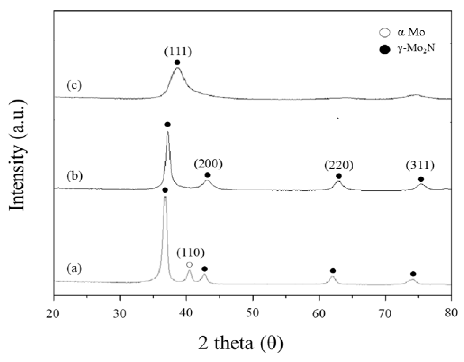
Figure 1. XRD patterns of the as-prepared MoN films deposited by (a) dcMS, (b) mfMS and (c) ICPMS.
Coatings 15 01155 g001
Figure 2. Residual stresses (compressive or tensile) of MoN films prepared by dcMS, mfMS and ICPMS.
Coatings 15 01155 g002
Figure 3. Microstructure through FE-SEM for the MoN film surface [(a) dcMS, (b) mfMS and (c) ICPMS] and cross-sectional FE-SEM [(d) dcMS, (e) mfMS and (f) ICPMS].
Coatings 15 01155 g003
Figure 4. Nanoindentation hardness and elastic modulus of MoN films prepared by dcMS, mfMS and ICPMS.
Coatings 15 01155 g004
Figure 5. Electrical resistivity of MoN films prepared by dcMS, mfMS and ICPMS.
Coatings 15 01155 g005
Table 1. Summary of deposition parameters.
MoNSputtering (Mode)
dcMSmfMSICPMS
Sputtering Power (W)300300300
ICP Power (W)--200
Pulse frequency (kHz)-15-
Duty cycle (%)-85-
Substrate bias voltage (V)−100−100−100
Substrate temperature (℃)400400400
Table 2. Lattice parameters of Υ-Mo2N films prepared by dcMS, mfMS and ICPMS.
MoN PhaseStructureLattice Plane Spacing (nm)Lattice Constants (nm)
Υ-Mo2N(dcMS)FCCd = 0.2442a = 0.4229
Υ-Mo2N(mfMS)FCCd = 0.2401a = 0.4159
Υ-Mo2N(ICPMS)FCCd = 0.2334a = 0.4043
Disclaimer/Publisher’s Note: The statements, opinions and data contained in all publications are solely those of the individual author(s) and contributor(s) and not of MDPI and/or the editor(s). MDPI and/or the editor(s) disclaim responsibility for any injury to people or property resulting from any ideas, methods, instructions or products referred to in the content.