Article

Two-Dimensional Crystal Growth of MoS2 Thin Films from Sodium Dodecyl Sulfate Micellar Solutions and Wettability Between Solution and Substrate

1
Department of Chemical Systems Engineering, Graduate School of Engineering, Nagoya University, Furo-cho, Chikusa-ku, Nagoya 464-8603, Japan
2
Institute of Innovation for Future Society, Nagoya University, Furo-cho, Chikusa-ku, Nagoya 464-8603, Japan
3
Department of International Collaborative Program in Sustainable Materials and Technology for Industries between Nagoya University and Chulalongkorn University, Graduate School of Engineering, Nagoya University, Furo-cho, Chikusa-ku, Nagoya 464-8603, Japan
4
Conjoint Research Laboratory in Nagoya University, Shinshu University, Furo-cho, Chikusa-ku, Nagoya 464-8603, Japan
*
Author to whom correspondence should be addressed.
Coatings 2025, 15(1), 4; https://doi.org/10.3390/coatings15010004
Submission received: 18 November 2024 / Revised: 18 December 2024 / Accepted: 21 December 2024 / Published: 24 December 2024

Abstract

:
In this study, the growth of 2D MoS2 thin films on SiO2/Si substrates was investigated using sodium dodecyl sulfate (SDS) micellar solutions, and the effects of SDS concentration and substrate treatment on crystal growth were evaluated. By increasing the SDS concentration, the wettability was improved, and uniform MoS2 crystal growth was promoted by micellar formation. When the SDS concentration exceeded 10−4 mol/L, the static contact angle sharply decreased, indicating uniform 2D material growth. The optimal conditions that enabled a uniform supply of Mo-based precursors were as follows: SDS concentration of 3.5 × 10⁻⁴ mol/L; Na2MoO4·2H2O concentration of 1.7 × 10⁻² mol/L. The results indicate that solution-based processes using SDS are effective for 2D material growth, and they may be a valuable technique in future thin film device fabrication processes.

1. Introduction

Transition metal dichalcogenides (e.g., MoS2, WS2, etc.), represented by the formula MX2 (where M is the transition metal, and X is the chalcogen element), are a class of layered materials that exhibit van der Waals heterostructures [1,2,3]. These heterostructures are formed by weak van der Waals forces between layers, allowing for the creation of stacked materials with unique electronic properties. In particular, bulk MoS2 transitions from an indirect bandgap (1.29 eV) to a direct bandgap (1.8 eV) when reduced to a monolayer [4,5,6]. MoS2 is favorable as a channel material for transistors because of its resistance to dangling bond formation [7,8]. Dangling bonds are unsatisfied atomic bonds that occur when atoms at the surface are not fully bonded, leading to defects. The ability of MoS2 to resist such bond formation minimizes surface defects, making it ideal for transistor applications. In addition, as semiconductor devices scale down below 5 nm, 2D MoS2 exhibits higher effective mobility than silicon, along with a lower tunneling leakage current [9,10]. Consequently, several researchers are exploring methods for producing high-quality MoS2 thin films.
However, achieving semiconductor-grade MoS2 thin films on a wafer scale remains challenging. Two-dimensional MoS2 can be fabricated using different techniques such as mechanical exfoliation, ion intercalation, physical vapor deposition (PVD), chemical vapor deposition (CVD), and thermal annealing of spin-coated films [11,12,13,14,15,16,17,18,19,20,21,22,23]. Among these methods, CVD is commonly used for both graphene preparation and mass production. However, in the CVD synthesis of graphene using segregation or catalytic functions for carbon atoms, transition metal substrates are generally used [24], but in the CVD synthesis of MoS2, substrates such as SiO2/Si, sapphire, and even molten glass are usually used [25,26]. However, from the perspective of the practice of following conventional semiconductor processes, growth on SiO2/Si is industrially important. Furthermore, SiO2/Si substrates are also commonly used because of the good visibility of 2D-MoS2/SiO2/Si under optical microscopes. Solution-based spin-coating followed by thermal annealing has received considerable attention because of its cost-effectiveness and ease of dopant introduction. This method often results in mixed 2D and 3D growth modes, making it difficult to achieve high-quality crystals comparable to those produced via CVD.
Liu et al. synthesized polycrystalline MoS2 thin films by coating a substrate with a solvent and performing two-step annealing under Ar/H2 and Ar/Ar+S atmospheres [27]. They emphasized the importance of an appropriate annealing temperature for achieving high crystallinity in solution-processed MoS2 films. Vapor–liquid–solid technology has been reported to be able to form larger single-crystal MoS2 monolayers [28]. Unlike silicon and other thin films where covalent bonds are formed between the thin film and the substrate, in MoS2 monolayers, weak interactions (van der Waals forces) are formed between the sulfur and the substrate. For this reason, the liquid–solid interface, which has high density and polarization, is thought to be very important for 2D crystal formation. On the other hand, this weak interaction can solve many problems related to heteroepitaxy [29,30]. However, this weak interaction also makes 2D growth difficult to control. In other words, the problem is how to control this interaction. Recent research has focused on controlling crystal growth by adding surfactants or other additives to the solution. For example, Zhu et al. achieved the creation of high-quality, large-area MoS2 monolayers by adding KOH to the solution [31]. In addition, 2D crystal growth can be enhanced by adding potassium or sodium ion [18,25,32,33,34]. Increasing the hydrophilicity of the substrate through wet chemical or UV treatment has also been reported to facilitate 2D crystal growth [25,35]. Esposito et al. also further focused on the role that density gradient mediums played in the sulfurization process, and demonstrated that these density gradient mediums can also affect the sizes, strains, and point-defects of the resulting MoS2 crystals [36].
Moreover, solution-based crystal growth can be regulated by controlling the surface tension of the solution and the surface energy of the substrate. This principle is similar to the use of surfactants in electroplating to control surface tension. Surfactants such as sodium dodecyl sulfate (SDS), cetyltrimethylammonium bromide (CTAB), and polyvinylpyrrolidone (PVP) are commonly used in electroplating to control surface tension and substrate surface energy [37,38,39,40]. SDS is selected over other surfactants because of its anionic nature, which prevents adsorption onto hydrophilic surfaces such as silanol groups on silicon substrates. In addition, SDS forms micelles, which can enhance wettability and promote uniform crystal growth. However, during high-temperature (>700 °C) sulfurization, the initial state of the solution and substrate surface does not affect crystal growth, and studies in this area are limited. By contrast, in ceramic sintering, the dispersion state of the slurry is critical to the final microstructure [41,42]. Therefore, elucidating the role of additives in promoting 2D MoS2 growth is necessary.
In this study, the role of additives in promoting 2D MoS2 growth was investigated by spin-coating SDS-containing solutions commonly used in electroplating onto SiO2/Si substrates, followed by sulfurization to form 2D MoS2 films. This study aimed to clarify the relationship between growth and wettability. In the absence of effective solutions for increasing crystal size in CVD and PVD, the liquid-phase process in this study has the potential to increase crystal size, and it is important both academically and industrially to work out the details of controlling the liquid-phase process.

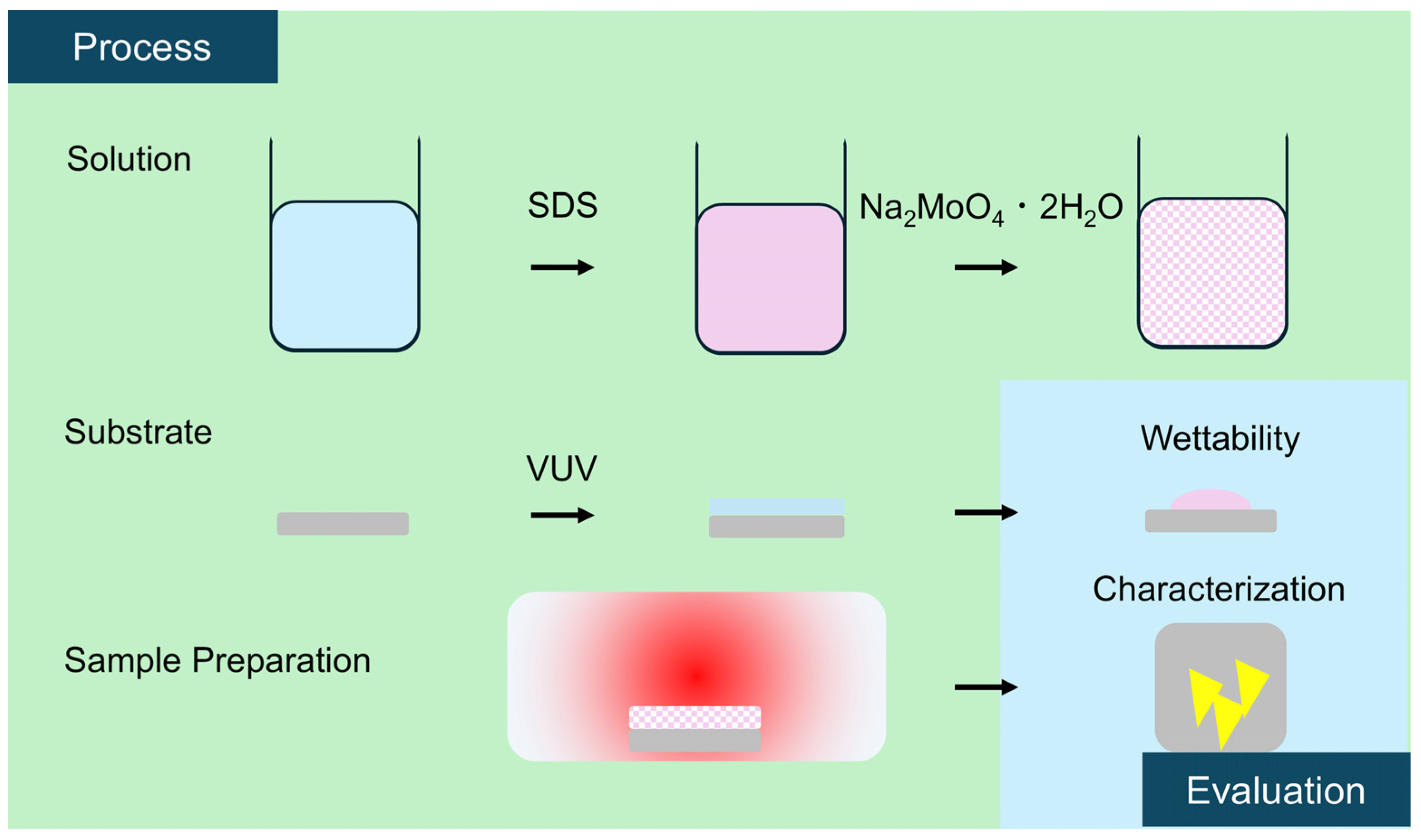
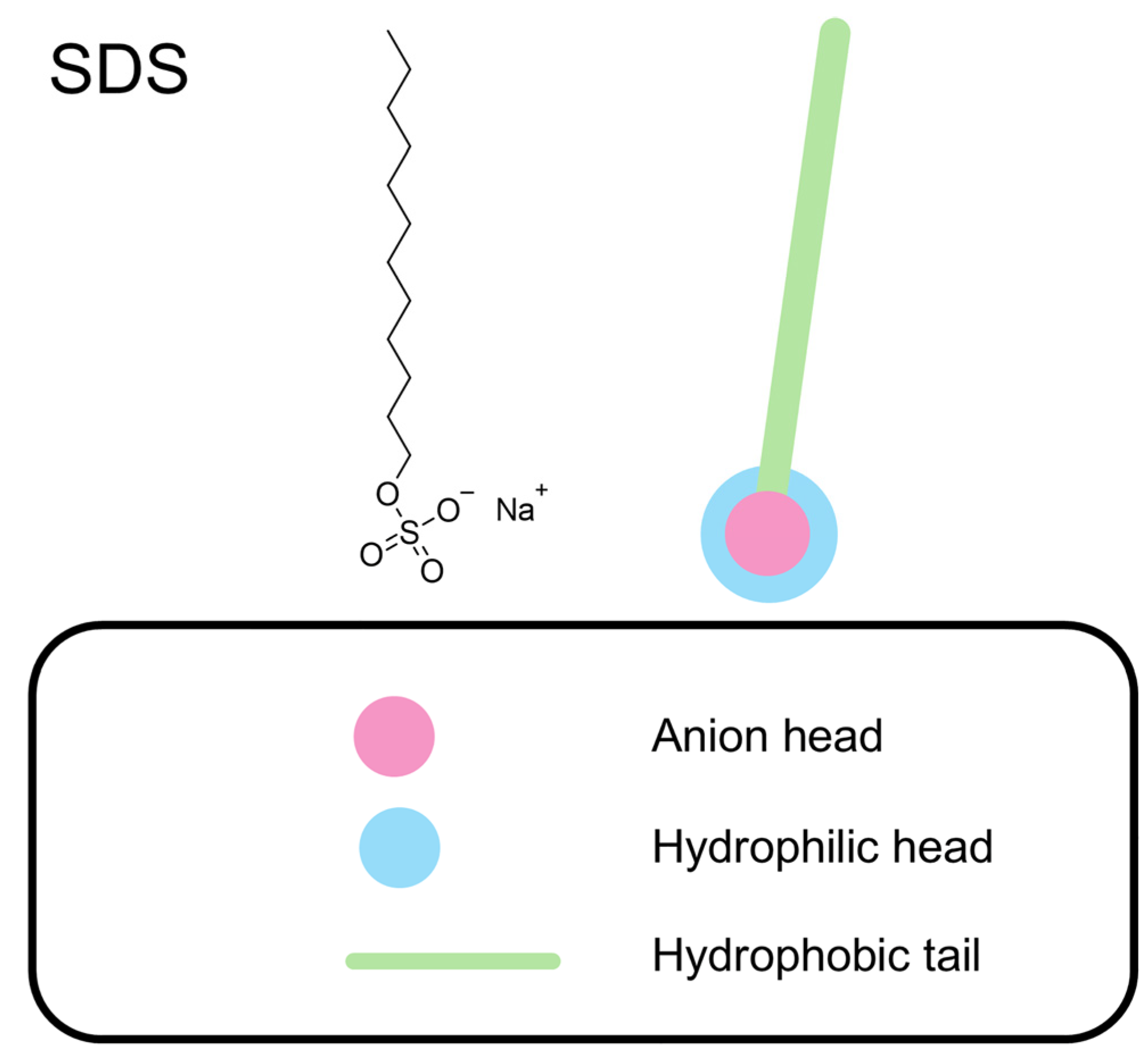
2. Materials and Methods

The experimental procedure is shown in Figure 1. Silicon wafers with a 300 nm thick SiO2 layer (10 mm2, Canosis Co., Ltd., Tokyo, Japan) were used as substrates. The substrates were hydrophilized by vacuum ultraviolet (VUV) irradiation using a xenon excimer lamp (USHIO, SH-172C, wavelength 172 nm, Tokyo, Japan). The substrates were placed in a vacuum chamber and irradiated at 100 Pa for 10 min. For the spin-coating solution, sodium molybdate dihydrate (Na2MoO4·2H2O, purity > 99%, Kanto Chemical, Tokyo, Japan) was mixed with a dispersing agent and ultrasonically stirred for 30 min. Sodium dodecyl sulfate (purity >99.0%, Sigma-Aldrich, Louis, MO, USA) was used as the dispersant. Sodium molybdate concentrations were adjusted to five levels: 8.3 × 10⁻³, 1.7 × 10⁻², 2.5 × 10⁻², 4.1 × 10⁻², and 8.3 × 10⁻² (mol/L). In addition, SDS concentrations were adjusted to five levels: 3.5 × 10⁻⁵, 1.7 × 10⁻⁴, 3.5 × 10⁻⁴, 6.9 × 10⁻⁴, and 3.5 × 10⁻³ (mol/L).
The prepared solution was spin-coated onto the substrate using a spin-coater (MIKASA Co., Ltd., MS-B100, Tokyo, Japan). During spin-coating, the rotation speed was increased to 5000 rpm for 10 s; this speed was maintained for another 10 s and then stopped. After spin-coating, the samples were dried in an oven at 90 °C for 30 min. Then, the spin-coated samples were placed in a tube furnace together with 500 mg of sulfur powder (purity > 99.5%, Kanto Chemical, Tokyo, Japan), and sulfurization was performed at 750 °C in accordance with previous studies [43]. After evacuating the furnace to approximately 20 Pa, argon gas was used to return the pressure to atmospheric levels. Evacuation and repressurization were repeated two times, followed by the introduction of 30 sccm of argon as a carrier gas. Sulfur (orthorhombic) has a melting point of 113 °C and a boiling point of 445 °C. The sulfur source was controlled at about 170 °C and was in the liquid phase. Therefore, sulfur gas was supplied at a vapor pressure below the saturated vapor pressure at 170 °C. On the other hand, the melting point of Na2MoO4 is 687 °C, and it gradually changes phase with the liquid on the substrate. Therefore, Na2MoO4 (l) was distributed on the substrate. In this sulfurization process, it can be predicted that the heterogeneous reaction between sulfur gas and this liquid will reduce Na2MoO4 to produce MoS2 and sodium oxide (Na2O), and the resulting Na2O reacts with the silica surface (SiO2) to form silicate (Na2SiO3) [44]. These reactions are as follows:
S s > 113   ° C S ( l ) S l 170   ° C S 2 ( g ) N a 2 M o O 4 ( s ) N a 2 M o O 4 ( l ) S 2 g + N a 2 M o O 4 s > 684   ° C M o S 2 s + N a 2 O s + S O 3 ( g ) N a 2 O s + S i O 2 s ( s u r f a c e ) N a 2 S i O 3 s
The morphology of the samples was analyzed using a field-emission scanning electron microscope (S-4800, Hitachi, Tokyo, Japan) with an accelerating voltage of 15.0 kV and a working distance of 8.8–8.9 mm. The chemical bonding states of the samples were analyzed by using a Raman microscope (Renishaw inVia, England, UK). Raman analysis was performed using a 532 nm laser (with a maximum power of 150 mW, Samba, Cobolt, Sweden). Light microscopic images were obtained using a light microscope integrated with the Raman system. The static contact angle was measured using a digital optical camera and the level of substrate stage was adjusted and confirmed by a level gauge. The drop volume was 10 μL and the contact angle was calculated using spherical approximation.

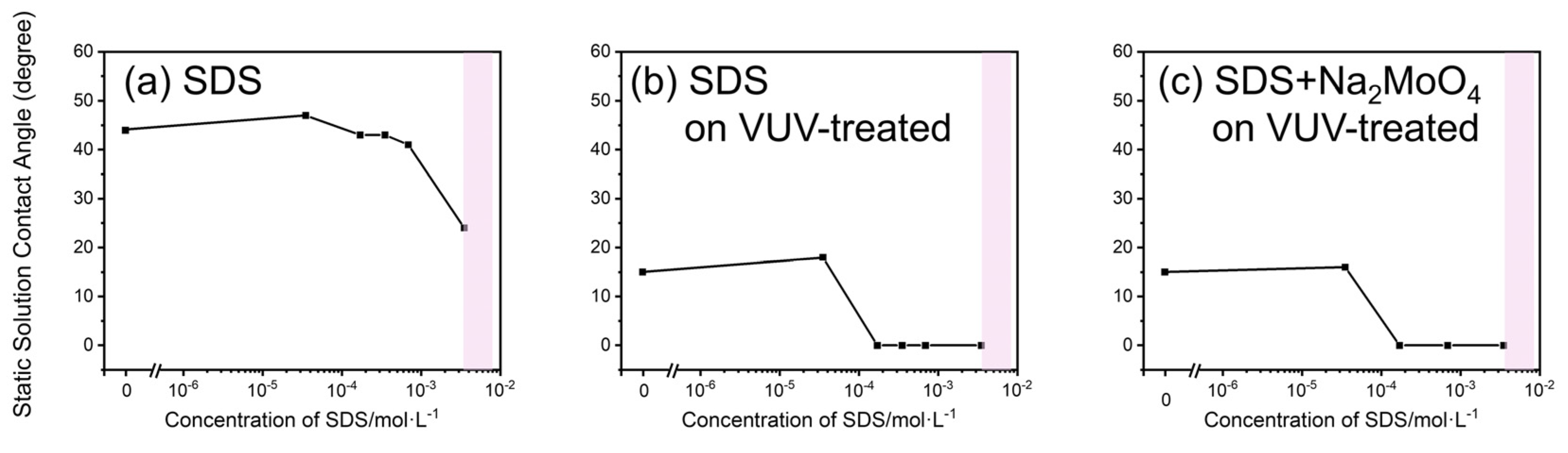
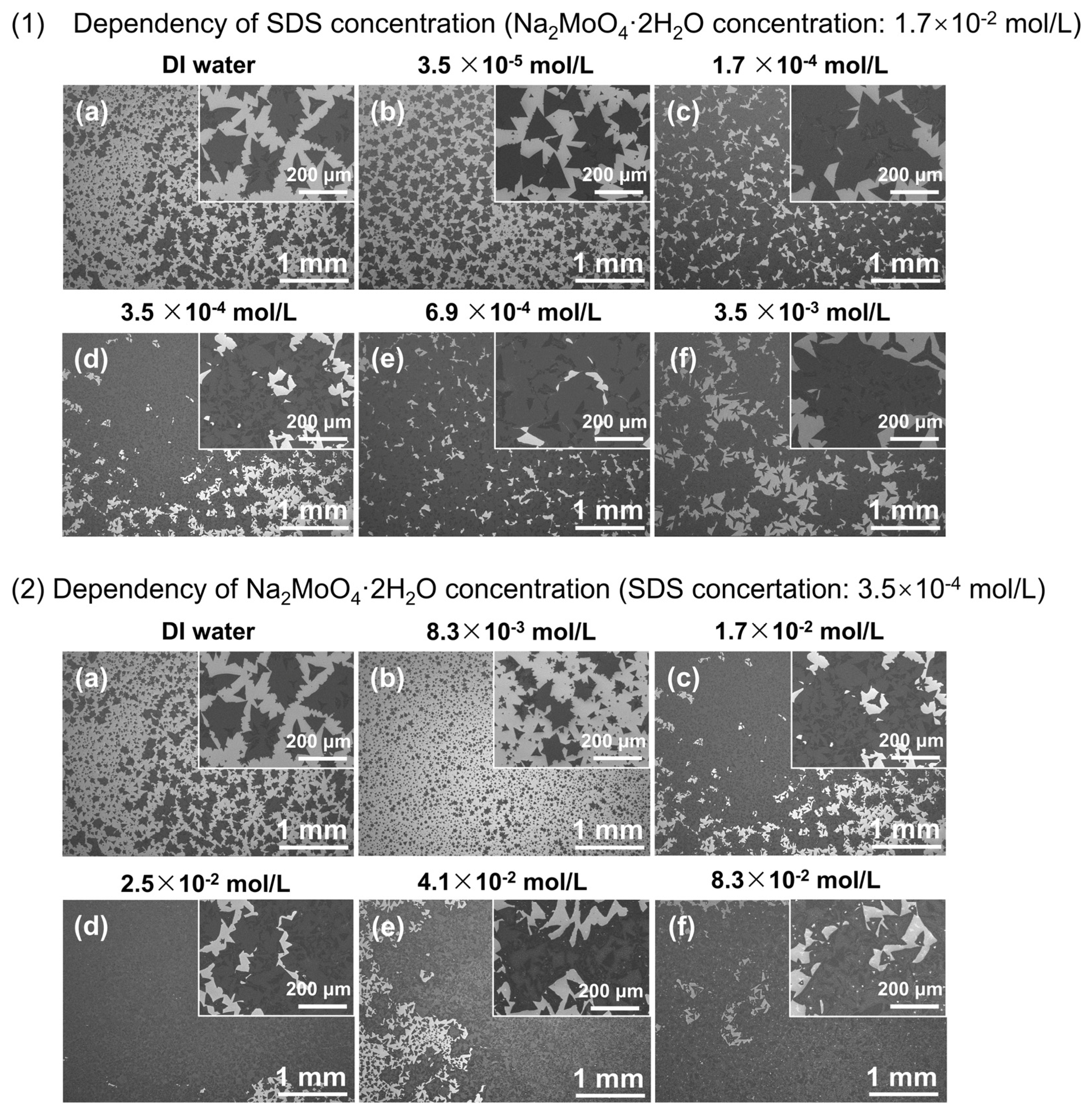
3. Results and Discussion

Figure 2 shows the molecular structure of SDS, highlighting the hydrophobic tail and the hydrophilic anionic head group. The anionic head forms the hydrophilic part of the molecule responsible for its interaction with the solution.
Figure 3 shows the static contact angles of aqueous SDS solutions under three conditions: (a) on substrates without VUV treatment, (b) on substrates with VUV treatment, and (c) on VUV-treated substrates with SDS/Na2MoO4·2H2O solution. The original static contact angles photos can be found in Figure S1. In addition, the contact angle obtained here can be ignored because the surface roughness of the silicon wafer used in this experiment is in the nanometer range. The pink band shown in Figure 3 represents the critical micelle concentration (CMC) of SDS in the solution [45,46]. The CMC refers to the concentration at which surfactant molecules begin to aggregate and form micelles in the solution. As shown in Figure 3a, the static contact angle decreased from about 45° to 30° with the increase in SDS concentration, indicating improved wettability caused by the addition of SDS, although the wettability was not significantly high.
Then, the static contact angle was measured on the VUV-treated substrates. The VUV treatment removed hydrocarbon contamination from the substrate surface and made it hydrophilic by generating silanol groups [47]. Consequently, the static contact angle decreased sharply as the SDS concentration exceeded 10−4 mol/L and approached zero at higher concentrations. This sharp decrease in the static contact angle was due to an increase in surface hydrophilicity, resulting from changes in surface energy after VUV treatment, which made the substrate more water attractive. Therefore, 10−4 mol/L is the CMC for this system.
At low SDS concentrations, an SDS monolayer is formed at the air–liquid interface, which reduces the static contact angle. At high SDS concentrations, micelles are formed in the solution, thereby reducing the static contact angle and surface tension. Micellar formation at concentrations below the typical CMC is likely due to electrostatic repulsion between the anionic silanol groups on the surface and the anionic SDS head groups [48,49,50,51,52]. Micellar formation in a solution is energetically more favorable than surface adsorption. Next, the effect of adding Na2MoO4·2H2O as the MoS2 precursor on wettability was investigated. The results indicated that wettability was primarily determined by the SDS concentration, regardless of the presence of Na2MoO4·2H2O. Therefore, SDS micelles facilitate the uniform distribution of MoO42− ions throughout the solution, leading to homogeneous growth over the entire surface. The micelles, with their hydrophilic heads, encapsulate and transport the MoO42− ions, allowing them to be evenly dispersed in the solution and uniformly delivered to the substrate. If this hypothesis is correct, then the crystal growth of MoS2 would be more uniform and two dimensional at SDS concentrations above the CMC.
Figure 4 shows the SEM images of MoS2 crystals at a fixed Na2MoO4·2H2O concentration of 1.7 × 10⁻² mol/L and varying SDS concentrations, as well as at a fixed SDS concentration of 3.5 × 10⁻⁴ mol/L and varying Na2MoO4·2H2O concentrations. As shown in Figure 4, the uniform coverage of crystalline MoS2 was observed even at the scale of several millimeters under all concentration conditions. In Figure 4(1), the size of the MoS2 crystals exceeded 200 μm at an SDS concentration of 1.7 × 10⁻⁴ mol/L, and 2D preferential growth was observed. In addition, the MoS2 coverage rate in the low-magnification SEM images (scale bar = 1 mm) was calculated using ImageJ software, and the results are shown in Table 1 and Table 2. As a result, the millimeter scale coverage rate was only 40.5% for the sample prepared with DI water, but the sample with added SDS showed a higher coverage rate than the sample without added SDS. This high coverage rate is extremely important for potential applications in the semiconductor industry. When the SDS concentration exceeded the CMC (3.5 × 10⁻⁴ mol/L), the crystal coverage increased with the increase in Na2MoO4·2H2O concentration, indicating that MoO42− ions were uniformly supplied to the entire substrate. In addition, even at the low coverage (24.0%) of the sample in Figure 4(2b), the 2D MoS2 crystals were uniformly distributed on the substrate. From the above, it is clear that the increase in wettability caused by SDS makes a significant contribution to uniformity.
Figure 5 shows the Raman spectroscopy results for different SDS (1) and Na2MoO4·2H2O (2) concentrations. The Raman spectra were measured at the center of each optical microscopic image. The typical Raman modes of MoS2, namely A1g and E12g, were measured, and the difference in Raman shift between the two modes was used to estimate the number of layers.
In the optical microscopic images, the bright regions (B1) were identified as bulk MoS2 based on the Raman spectra. The relatively dark areas (D1) corresponded to MoS2 with 2–4 layers, whereas the darker areas (D2) were identified as monolayer MoS2 [53,54]. The brightest areas (D3) indicated the bare SiO2 surface without MoS2 layers. For clarity, the SiO2 surface was marked with a purple mask in the optical images. The purple mask was applied to the area (D1) to make it easier to distinguish.
When the SDS concentration was zero (Figure 5(1)), large areas of bulk MoS2 were observed. At an SDS concentration of 3.5 × 10⁻⁵ mol/L, the formation of bulk MoS2 was suppressed, although the crystal size did not increase. When the SDS concentration was further increased to 3.5 × 10⁻⁴ mol/L, the entire substrate was covered with MoS2, although the number of layers also increased, as indicated by the growth in regions (D1) and (B1).
When the Na2MoO4·2H2O concentration was varied (Figure 5(2)), MoS2 crystals covered the entire substrate at 1.7 × 10⁻² mol/L. At lower concentrations, the areas of exposed SiO2 were prominent, whereas, at higher Na2MoO4·2H2O concentrations, the size of regions (B1) and (D1) increased. This finding indicates that the balance between SDS and Na2MoO4·2H2O concentrations determines not only the uniformity of MoO42− ion supply, but also the uniformity of MoS2 crystal growth.
Based on these results, the optimal conditions for the uniform supply of Mo-based precursors throughout the substrate were as follows: an SDS concentration of 3.5 × 10⁻⁴ mol/L and a Na2MoO4·2H2O concentration of 1.7 × 10⁻² mol/L. This phenomenon may be due to the surface charges of silanol groups, the charge of SDS, and the formation of micelles (Figure 6). However, the range of MoO42− ion concentrations suitable for uniform growth is limited. Future work should focus on optimizing the surfactant by introducing branched structures to the hydrophobic tail of SDS, thereby increasing the solvent exclusion volume of the micelle. The potential application of micelle-based solvents in controlling MoS2 crystal growth also warrants further investigation.

4. Conclusions

In this study, the growth of 2D MoS2 thin films was investigated using SDS micellar solutions, and the effects of SDS concentration and substrate surface treatment on crystal growth were evaluated. We confirmed that SDS improved wettability and promoted MoS2 crystal growth through micellar formation in a solution. When the SDS concentration exceeded 10−4 mol/L, the static contact angle decreased sharply, enabling the uniform 2D growth of MoS2 on the substrate. In addition, by optimizing the concentration of Na2MoO4·2H2O, MoO42− ions could be supplied uniformly over the surface, allowing for controlled crystal size.
The optimal growth conditions were as follows: SDS concentration of 3.5 × 10⁻⁴ mol/L and Na2MoO4·2H2O concentration of 1.7 × 10⁻² mol/L. These results indicate that using SDS is effective for low-cost and efficient growth of 2D materials, making it a promising approach for future thin film fabrication. The results of this study show that general additives such as KOH can preferentially induce a 2D growth mode due to their anion-wetting-promoting effect at high temperatures, but that SDS can control both the wettability of the solution and substrate at room temperature and the anion-wetting-promoting effect at high temperatures. In other words, the simultaneous control of the substrate coating process and the crystallization process in the solution method will be the basis for producing even higher quality MoS2 crystals in the future. Moreover, further optimization of material synthesis based on micellar formation could promote advanced control of crystal growth.

Supplementary Materials

The following supporting information can be downloaded at: https://www.mdpi.com/article/10.3390/coatings15010004/s1, Figure S1: Original static contact angles photos in Figure 3: (a) on substrates without vacuum ultraviolet (VUV) treatment, (b) on substrates with VUV treatment, and (c) on VUV-treated substrates with SDS/Na2MoO4·2H2O solution.

Author Contributions

Conceptualization, Z.Z. and N.S.; methodology, Z.Z. and Y.L.; validation, Z.Z., Y.L., Y.S. and N.S.; investigation, Z.Z.; resources, Z.Z., Y.L., Y.S. and N.S.; data curation, Z.Z., Y.L. and Y.S.; writing—original draft preparation, Z.Z.; writing—review and editing, N.S.; visualization, Z.Z.; supervision, Y.S. and N.S.; project administration, Z.Z. and N.S.; funding acquisition, N.S. All authors have read and agreed to the published version of the manuscript.

Funding

This paper is based on the results obtained from “Research and Development Project of the Enhanced Infrastructures for Post-5G Information and Communication Systems” (JPNP20017), commissioned by the New Energy and Industrial Technology Development Organization (NEDO).

Institutional Review Board Statement

Not applicable.

Informed Consent Statement

Not applicable.

Data Availability Statement

Data are contained within the article.

Acknowledgments

Zhunda Zhu is also supported by a scholarship from the China Scholarship Council (CSC, No. CSC202006130019). We extend our gratitude to the CSC for the financial support provided to Zhunda Zhu.

Conflicts of Interest

The authors declare no conflicts of interest.

References

  1. Novoselov, K.S.; Mishchenko, A.; Carvalho, A.; Neto, A.H.C. 2D materials and van der Waals heterostructures. Science 2016, 353, aac9439. [Google Scholar] [CrossRef] [PubMed]
  2. Seravalli, L.; Bosi, M. A Review on Chemical Vapour Deposition of Two-Dimensional MoS2 Flakes. Materials 2021, 14, 7590. [Google Scholar] [CrossRef] [PubMed]
  3. Bianco, G.V.; Losurdo, M.; Giangregorio, M.M.; Sacchetti, A.; Prete, P.; Lovergine, N.; Capezzuto, P.; Bruno, G. Direct epitaxial CVD synthesis of tungsten disulfide on epitaxial and CVD graphene. RSC Adv. 2015, 5, 98700–98708. [Google Scholar] [CrossRef]
  4. Yoon, Y.; Ganapathi, K.; Salahuddin, S. How Good Can Monolayer MoS2 Transistors Be? Nano Lett. 2011, 11, 3768–3773. [Google Scholar] [CrossRef]
  5. Splendiani, A.; Sun, L.; Zhang, Y.; Li, T.; Kim, J.; Chim, C.-Y.; Galli, G.; Wang, F. Emerging Photoluminescence in Monolayer MoS2. Nano Lett. 2010, 10, 1271–1275. [Google Scholar] [CrossRef] [PubMed]
  6. Mak, K.F.; Lee, C.; Hone, J.; Shan, J.; Heinz, T.F. Atomically ThinMoS2: A New Direct-Gap Semiconductor. Phys. Rev. Lett. 2010, 105, 136805. [Google Scholar] [CrossRef] [PubMed]
  7. Radisavljevic, B.; Radenovic, A.; Brivio, J.; Giacometti, V.; Kis, A. Single-layer MoS2 transistors. Nat. Nanotechnol. 2011, 6, 147–150. [Google Scholar] [CrossRef] [PubMed]
  8. Wu, F.; Tian, H.; Shen, Y.; Hou, Z.; Ren, J.; Gou, G.; Sun, Y.; Yang, Y.; Ren, T.-L. Vertical MoS2 transistors with sub-1-nm gate lengths. Nature 2022, 603, 259–264. [Google Scholar] [CrossRef]
  9. Liu, Y.; Duan, X.; Shin, H.-J.; Park, S.; Huang, Y.; Duan, X. Promises and prospects of two-dimensional transistors. Nature 2021, 591, 43–53. [Google Scholar] [CrossRef]
  10. Desai, S.B.; Madhvapathy, S.R.; Sachid, A.B.; Llinas, J.P.; Wang, Q.; Ahn, G.H.; Pitner, G.; Kim, M.J.; Bokor, J.; Hu, C.; et al. MoS 2 transistors with 1-nanometer gate lengths. Science 2016, 354, 99–102. [Google Scholar] [CrossRef] [PubMed]
  11. Liu, N.; Kim, P.; Kim, J.H.; Ye, J.H.; Kim, S.; Lee, C.J. Large-Area Atomically Thin MoS2 Nanosheets Prepared Using Electrochemical Exfoliation. ACS Nano 2014, 8, 6902–6910. [Google Scholar] [CrossRef]
  12. Shi, J.; Yang, Y.; Zhang, Y.; Ma, D.; Wei, W.; Ji, Q.; Zhang, Y.; Song, X.; Gao, T.; Li, C.; et al. Monolayer MoS2 Growth on Au Foils and On-Site Domain Boundary Imaging. Adv. Funct. Mater. 2014, 25, 842–849. [Google Scholar] [CrossRef]
  13. Li, H.; Wu, J.; Yin, Z.; Zhang, H. Preparation and Applications of Mechanically Exfoliated Single-Layer and Multilayer MoS2and WSe2Nanosheets. Accounts Chem. Res. 2014, 47, 1067–1075. [Google Scholar] [CrossRef]
  14. Cheng, Q.; Pang, J.; Sun, D.; Wang, J.; Zhang, S.; Liu, F.; Chen, Y.; Yang, R.; Liang, N.; Lu, X.; et al. WSe2 2D p-type semiconductor-based electronic devices for information technology: Design, preparation, and applications. InfoMat 2020, 2, 656–697. [Google Scholar] [CrossRef]
  15. Lu, Y.; Chen, T.; Ryu, G.H.; Huang, H.; Sheng, Y.; Chang, R.-J.; Warner, J.H. Self-Limiting Growth of High-Quality 2D Monolayer MoS2 by Direct Sulfurization Using Precursor-Soluble Substrates for Advanced Field-Effect Transistors and Photodetectors. ACS Appl. Nano Mater. 2018, 2, 369–378. [Google Scholar] [CrossRef]
  16. Wang, Q.; Li, N.; Tang, J.; Zhu, J.; Zhang, Q.; Jia, Q.; Lu, Y.; Wei, Z.; Yu, H.; Zhao, Y.; et al. Wafer-Scale Highly Oriented Monolayer MoS2 with Large Domain Sizes. Nano Lett. 2020, 20, 7193–7199. [Google Scholar] [CrossRef] [PubMed]
  17. Yu, H.; Liao, M.; Zhao, W.; Liu, G.; Zhou, X.J.; Wei, Z.; Xu, X.; Liu, K.; Hu, Z.; Deng, K.; et al. Wafer-Scale Growth and Transfer of Highly-Oriented Monolayer MoS2 Continuous Films. ACS Nano 2017, 11, 12001–12007. [Google Scholar] [CrossRef] [PubMed]
  18. Patel, C.; Singh, R.; Dubey, M.; Pandey, S.K.; Upadhyay, S.N.; Kumar, V.; Sriram, S.; Htay, M.T.; Pakhira, S.; Atuchin, V.V.; et al. Large and Uniform Single Crystals of MoS2 Monolayers for ppb-Level NO2 Sensing. ACS Appl. Nano Mater. 2022, 5, 9415–9426. [Google Scholar] [CrossRef]
  19. Kim, H.; Ahn, C.; Arabale, G.; Lee, C.; Kim, T. Synthesis of MoS2 Atomic Layer using PECVD. ECS Trans. 2013, 58, 47–50. [Google Scholar] [CrossRef]
  20. Ahn, C.; Lee, J.; Kim, H.; Bark, H.; Jeon, M.; Ryu, G.H.; Lee, Z.; Yeom, G.Y.; Kim, K.; Jung, J.; et al. Low-Temperature Synthesis of Large-Scale Molybdenum Disulfide Thin Films Directly on a Plastic Substrate Using Plasma-Enhanced Chemical Vapor Deposition. Adv. Mater. 2015, 27, 5223–5229. [Google Scholar] [CrossRef] [PubMed]
  21. Bala, A.; Liu, N.; Sen, A.; Cho, Y.; Pujar, P.; So, B.; Kim, S. Low-Temperature Plasma-Assisted Growth of Large-Area MoS2 for Transparent Phototransistors. Adv. Funct. Mater. 2022, 32, 2205106. [Google Scholar] [CrossRef]
  22. Choi, J.; Ha, M.; Park, J.C.; Park, T.J.; Kim, W.; Lee, M.; Ahn, J. A Strategy for Wafer-Scale Crystalline MoS2 Thin Films with Controlled Morphology Using Pulsed Metal–Organic Chemical Vapor Deposition at Low Temperature. Adv. Mater. Interfaces 2021, 9, 2101785. [Google Scholar] [CrossRef]
  23. Mun, J.; Park, H.; Park, J.; Joung, D.; Lee, S.-K.; Leem, J.; Myoung, J.-M.; Park, J.; Jeong, S.-H.; Chegal, W.C.; et al. High-Mobility MoS2 Directly Grown on Polymer Substrate with Kinetics-Controlled Metal–Organic Chemical Vapor Deposition. ACS Appl. Electron. Mater. 2019, 1, 608–616. [Google Scholar] [CrossRef]
  24. Zhang, Y.; Zhang, L.; Zhou, C. Review of Chemical Vapor Deposition of Graphene and Related Applications. Acc. Chem. Res. 2013, 46, 2329–2339. [Google Scholar] [CrossRef]
  25. Cun, H.; Macha, M.; Kim, H.; Liu, K.; Zhao, Y.; LaGrange, T.; Kis, A.; Radenovic, A. Wafer-scale MOCVD growth of monolayer MoS2 on sapphire and SiO2. Nano Res. 2019, 12, 2646–2652. [Google Scholar] [CrossRef]
  26. Zhang, Z.; Xu, X.; Song, J.; Gao, Q.; Li, S.; Hu, Q.; Li, X.; Wu, Y. High-performance transistors based on monolayer CVD MoS2 grown on molten glass. Appl. Phys. Lett. 2018, 113, 202103. [Google Scholar] [CrossRef]
  27. Liu, K.-K.; Zhang, W.; Lee, Y.-H.; Lin, Y.-C.; Chang, M.-T.; Su, C.-Y.; Chang, C.-S.; Li, H.; Shi, Y.; Zhang, H.; et al. Growth of Large-Area and Highly Crystalline MoS2 Thin Layers on Insulating Substrates. Nano Lett. 2012, 12, 1538–1544. [Google Scholar] [CrossRef]
  28. Chang, M.-C.; Ho, P.-H.; Tseng, M.-F.; Lin, F.-Y.; Hou, C.-H.; Lin, I.-K.; Wang, H.; Huang, P.-P.; Chiang, C.-H.; Yang, Y.-C.; et al. Fast growth of large-grain and continuous MoS2 films through a self-capping vapor-liquid-solid method. Nat. Commun. 2020, 11, 1–9. [Google Scholar] [CrossRef] [PubMed]
  29. Lovergine, N.; Cingolani, R.; Mancini, A.; Ferrara, M. Photoluminescence of CVD grown CdS epilayers on CdTe substrates. J. Cryst. Growth 1992, 118, 304–308. [Google Scholar] [CrossRef]
  30. Lovergine, N.; Liaci, L.; Ganière, J.-D.; Leo, G.; Drigo, A.V.; Romanato, F.; Mancini, A.M.; Vasanelli, L. Inhomogeneous strain relaxation and defect distribution of ZnTe layers deposited on (100)GaAs by metalorganic vapor phase epitaxy. J. Appl. Phys. 1995, 78, 229–235. [Google Scholar] [CrossRef]
  31. Zhu, J.; Xu, H.; Zou, G.; Zhang, W.; Chai, R.; Choi, J.; Wu, J.; Liu, H.; Shen, G.; Fan, H. MoS2–OH Bilayer-Mediated Growth of Inch-Sized Monolayer MoS2 on Arbitrary Substrates. J. Am. Chem. Soc. 2019, 141, 5392–5401. [Google Scholar] [CrossRef] [PubMed]
  32. Kim, H.; Ovchinnikov, D.; Deiana, D.; Unuchek, D.; Kis, A. Suppressing Nucleation in Metal–Organic Chemical Vapor Deposition of MoS2 Monolayers by Alkali Metal Halides. Nano Lett. 2017, 17, 5056–5063. [Google Scholar] [CrossRef] [PubMed]
  33. Wang, P.; Lei, J.; Qu, J.; Cao, S.; Jiang, H.; He, M.; Shi, H.; Sun, X.; Gao, B.; Liu, W. Mechanism of Alkali Metal Compound-Promoted Growth of Monolayer MoS2: Eutectic Intermediates. Chem. Mater. 2019, 31, 873–880. [Google Scholar] [CrossRef]
  34. Singh, A.; Moun, M.; Sharma, M.; Barman, A.; Kapoor, A.K.; Singh, R. NaCl-assisted substrate dependent 2D planar nucleated growth of MoS2. Appl. Surf. Sci. 2020, 538, 148201. [Google Scholar] [CrossRef]
  35. Kwack, Y.-J.; Can, T.T.T.; Choi, W.-S. Bottom-up water-based solution synthesis for a large MoS2 atomic layer for thin-film transistor applications. npj 2D Mater. Appl. 2021, 5, 1–8. [Google Scholar] [CrossRef]
  36. Esposito, F.; Bosi, M.; Attolini, G.; Rossi, F.; Panasci, S.; Fiorenza, P.; Giannazzo, F.; Fabbri, F.; Seravalli, L. Role of density gradients in the growth dynamics of 2-dimensional MoS2 using liquid phase molybdenum precursor in chemical vapor deposition. Appl. Surf. Sci. 2023, 639, 158230. [Google Scholar] [CrossRef]
  37. Ye, W.; Ma, C.; Shang, W.; Chen, Y.; Wang, R.; Wang, C. Effect of sodium dodecylsulfate on improving microstructural properties of electroplated silver–oxygen–tungsten thin films. Surf. Coatings Technol. 2007, 201, 9456–9461. [Google Scholar] [CrossRef]
  38. Sciscenko, I.; Pedre, I.; Hunt, A.; Bogo, H.; González, G. Determination of a typical additive in zinc electroplating baths. Microchem. J. 2016, 127, 226–230. [Google Scholar] [CrossRef]
  39. Reid, J.D.; Zhou, J. Impact of Leveler Molecular Weight and Concentration on Damascene Copper Electroplating. ECS Trans. 2007, 2, 77–92. [Google Scholar] [CrossRef]
  40. Lin, C.; Liu, Y.; Zhang, X.; Miao, X.; Chen, Y.; Chen, S.; Zhang, Y. Regulating the plating process of zinc with highly efficient additive for long-life zinc anode. J. Power Sources 2022, 549, 232078. [Google Scholar] [CrossRef]
  41. Leo, S.; Tallon, C.; Stone, N.; Franks, G.V. Near-Net-Shaping Methods for Ceramic Elements of (Body) Armor Systems. J. Am. Ceram. Soc. 2014, 97, 3013–3033. [Google Scholar] [CrossRef]
  42. Mori, T.; Kitagawa, R. Experimental study on the time change in fluidity and particle dispersion state of alumina slurries with and without sintering aid. Ceram. Int. 2017, 43, 13422–13429. [Google Scholar] [CrossRef]
  43. Zhu, Z.; Liu, Y.; Sato, K.; Niu, J.; Chokradjaroen, C.; Sawada, Y.; Saito, N. Few-Layer MoS2 on a SiO2/Si Wafer through Sulfurization Chemical Vapor Deposition with a Vaporization-Shadowing Effect. ACS Appl. Nano Mater. 2024, 7, 20257–20266. [Google Scholar] [CrossRef]
  44. Kalt, R.A.; Arcifa, A.; Wäckerlin, C.; Stemmer, A. CVD of MoS2 single layer flakes using Na2MoO4 – impact of oxygen and temperature–time-profile. Nanoscale 2023, 15, 18871–18882. [Google Scholar] [CrossRef] [PubMed]
  45. Nivón-Ramírez, D.; Reyes-García, L.I.; Oviedo-Roa, R.; Gómez-Balderas, R.; Zuriaga-Monroy, C.; Martínez-Magadán, J.-M. Critical Micelle Concentration of SDS Through DPD Simulations Using COSMO-RS–Based Interaction Parameters, the Thermal Effects. Colloids Surf. A Physicochem. Eng. Asp. 2022, 645, 128867. [Google Scholar] [CrossRef]
  46. Bahri, M.A.; Hoebeke, M.; Grammenos, A.; Delanaye, L.; Vandewalle, N.; Seret, A. Investigation of SDS, DTAB and CTAB micelle microviscosities by electron spin resonance. Colloids Surfaces A Physicochem. Eng. Asp. 2006, 290, 206–212. [Google Scholar] [CrossRef]
  47. Sugimura, H.; Saito, N.; Maeda, N.; Ikeda, I.; Ishida, Y.; Hayashi, K.; Hong, L.; Takai, O. Surface potential microscopy for chemistry of organic self-assembled monolayers in small domains. Nanotechnology 2004, 15, S69–S75. [Google Scholar] [CrossRef]
  48. Kumar, N.; Varanasi, K.; Tilton, R.D.; Garoff, S. Surfactant Self-Assembly ahead of the Contact Line on a Hydrophobic Surface and Its Implications for Wetting. Langmuir 2003, 19, 5366–5373. [Google Scholar] [CrossRef]
  49. Frank, B.; Garoff, S. Surfactant self-assembly near contact lines: Control of advancing surfactant solutions. Colloids Surfaces A Physicochem. Eng. Asp. 1996, 116, 31–42. [Google Scholar] [CrossRef]
  50. Starov, V.; Ivanova, N.; Rubio, R.G. Why do aqueous surfactant solutions spread over hydrophobic substrates? Adv. Colloid Interface Sci. 2010, 161, 153–162. [Google Scholar] [CrossRef]
  51. Penta, N.K.; Amanapu, H.; Peethala, B.; Babu, S. Use of anionic surfactants for selective polishing of silicon dioxide over silicon nitride films using colloidal silica-based slurries. Appl. Surf. Sci. 2013, 283, 986–992. [Google Scholar] [CrossRef]
  52. Starov, V.M.; Kosvintsev, S.R.; Velarde, M.G. Spreading of Surfactant Solutions over Hydrophobic Substrates. J. Colloid Interface Sci. 2000, 227, 185–190. [Google Scholar] [CrossRef] [PubMed]
  53. Luo, R.; Xu, W.W.; Zhang, Y.; Wang, Z.; Wang, X.; Gao, Y.; Liu, P.; Chen, M. Van der Waals interfacial reconstruction in monolayer transition-metal dichalcogenides and gold heterojunctions. Nat. Commun. 2020, 11, 1–12. [Google Scholar] [CrossRef] [PubMed]
  54. Panasci, S.E.; Schilirò, E.; Greco, G.; Cannas, M.; Gelardi, F.M.; Agnello, S.; Roccaforte, F.; Giannazzo, F. Strain, Doping, and Electronic Transport of Large Area Monolayer MoS2 Exfoliated on Gold and Transferred to an Insulating Substrate. ACS Appl. Mater. Interfaces 2021, 13, 31248–31259. [Google Scholar] [CrossRef] [PubMed]
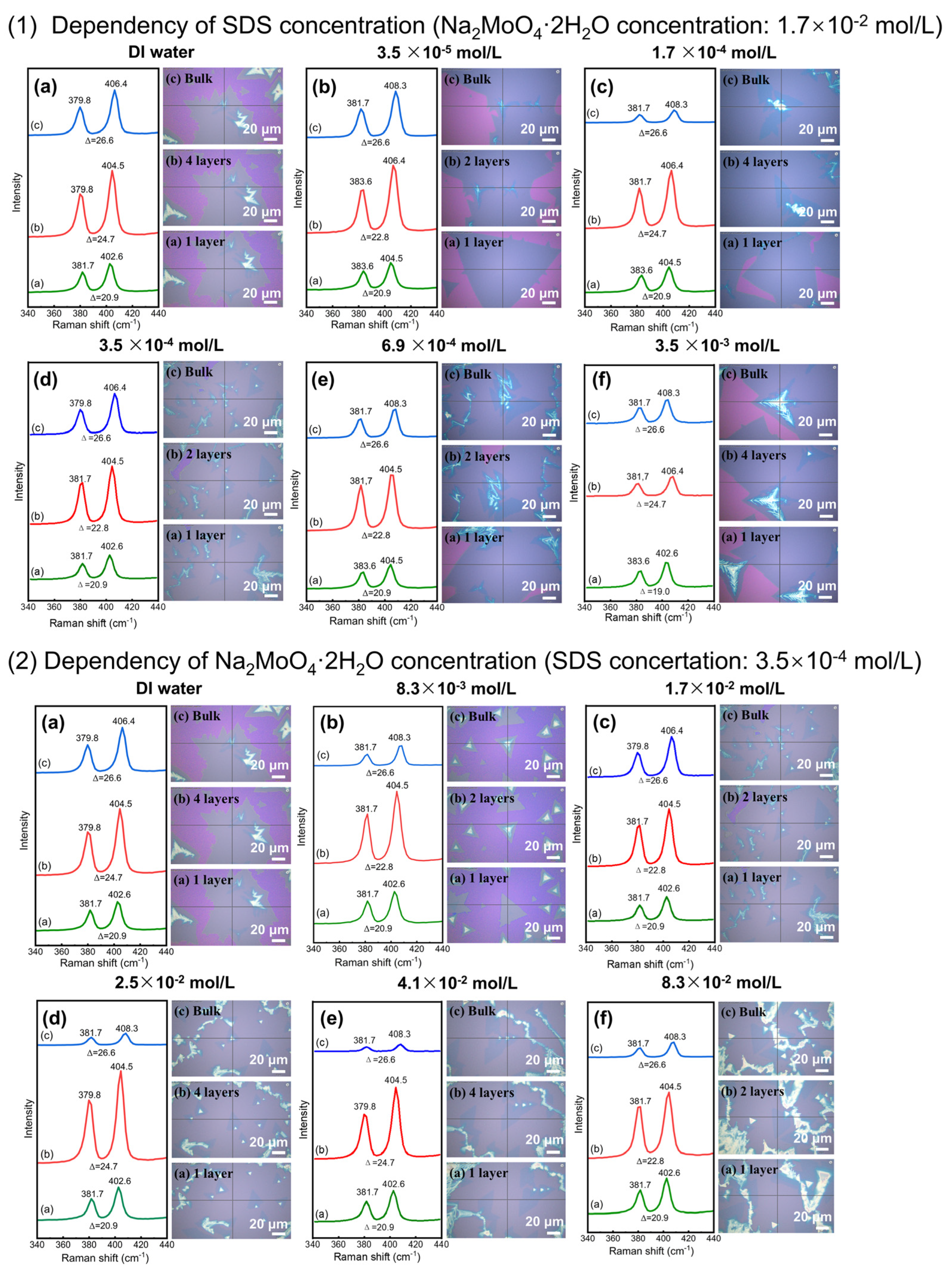
Figure 1. Schematic illustration of the experimental process.
Coatings 15 00004 g001
Figure 2. Molecular structure of SDS and illustration of its hydrophobic tail and hydrophilic anionic head group.
Coatings 15 00004 g002
Figure 3. Static contact angles of aqueous SDS solutions under three conditions: (a) on substrates without vacuum ultraviolet (VUV) treatment, (b) on substrates with VUV treatment, and (c) on VUV-treated substrates with SDS/Na2MoO4·2H2O solution.
Coatings 15 00004 g003
Figure 4. SEM images of MoS2 crystals at (1) a fixed Na2MoO4·2H2O concentration of 1.7 × 10⁻² mol/L and varying SDS concentrations (DI water, 3.5 × 10⁻⁵, 1.7 × 10⁻⁴, 3.5 × 10⁻⁴, 6.9 × 10⁻⁴, and 3.5 × 10⁻³ mol/L from (af)), as well as at (2) a fixed SDS concentration of 3.5 × 10⁻⁴ mol/L and varying Na2MoO4·2H2O concentrations (DI water, 8.3 × 10⁻³, 1.7 × 10⁻², 2.5 × 10⁻², 4.1 × 10⁻², and 8.3 × 10⁻² mol/L from (af)).
Coatings 15 00004 g004
Figure 5. Raman spectroscopy of MoS2 crystals at (1) a fixed Na2MoO4·2H2O concentration of 1.7 × 10⁻² mol/L and varying SDS concentrations (DI water, 3.5 × 10⁻⁵, 1.7 × 10⁻⁴, 3.5 × 10⁻⁴, 6.9 × 10⁻⁴, and 3.5 × 10⁻³ mol/L from (af)), as well as at (2) a fixed SDS concentration of 3.5 × 10⁻⁴ mol/L and varying Na2MoO4·2H2O concentrations (DI water, 8.3 × 10⁻³, 1.7 × 10⁻², 2.5 × 10⁻², 4.1 × 10⁻², and 8.3 × 10⁻² mol/L from (af)).
Coatings 15 00004 g005
Figure 6. Electrostatic repulsion between the silanol groups on the SiO2 surface and the SDS head, as well as the formation of SDS micelles.
Coatings 15 00004 g006
Table 1. MoS2 coverages on SiO2/Si calculated from Figure 4(1): a fixed Na2MoO4·2H2O concentration of 1.7 × 10⁻² mol/L and varying SDS concentrations.
SDS Concentration (mol/L)DI Water3.5 × 10−51.7 × 10−43.5 × 10−46.9 × 10−43.5 × 10−3
Coverage40.5%49.9%82.1%85.1%92.8%76.9%
Coverages were obtained by ImageJ software (U. S. National Institutes of Health, Bethesda, MD, USA) (version 1.53t).
Table 2. MoS2 coverages on SiO2/Si calculated from Figure 4(2): a fixed SDS concentration of 3.5 × 10⁻⁴ mol/L and varying Na2MoO4·2H2O concentrations.
Na2MoO4·2H2O Concentration (mol/L)DI Water8.3 × 10−31.7 × 10−22.5 × 10−24.1 × 10−28.3 × 10−2
Coverage40.5%24.0%85.1%98.6%88.4%95.3%
Coverages were obtained by ImageJ software.
Disclaimer/Publisher’s Note: The statements, opinions and data contained in all publications are solely those of the individual author(s) and contributor(s) and not of MDPI and/or the editor(s). MDPI and/or the editor(s) disclaim responsibility for any injury to people or property resulting from any ideas, methods, instructions or products referred to in the content.

