1. Introduction
Cr-based coatings are attractive for research in anticorrosion applications [
1,
2]. The adhesion properties of these coatings are well-known [
3]. The study of their tribological characteristics has revealed that they extend the lifetime of industrial tools [
4]. Physical Vapour Deposition (PVD) techniques are widely applied to the deposition of Cr-based coatings—such as for applications in moulding [
5]—and to metal forming industries [
6], and they are also environmentally friendly alternatives to electroplating and electrolysis processing [
7]. Among the other PVD techniques, magnetron sputtering allows the deposition of Cr-based coatings with smooth surfaces and uniform coating thickness distribution on complex geometry components [
8]. Various reactive unbalanced magnetron sputtering techniques are attractive for the deposition of well-adhering and uniform coatings on large-area substrates with high purity in addition to high-density films at low temperatures. By an appropriate combination of process parameters like target sputtering power, gas flux, plasma density, substrate temperature, total pressure, etc., the microstructure, chemical composition, mechanical, optical, electrical, and magnetic characteristics of the deposited coatings [
9] can be readily modified. By changing the sputtering gas composition in CrN-based coating deposition, pure Cr, Cr
2N, and CrN phases can be formed [
10], and different mechanical properties can be obtained.
Although the mechanical, structural, and composition properties of these layers have been widely researched, further investigations of their optical properties are necessary. Techniques like in situ ellipsometry could provide insights when analysing the structure of complex materials and investigating the interactions during the deposition of thin films. The optical properties of thin films are affected by composition, thickness, conductivity, and porosity, and ellipsometry measurements, and analysis can deliver this information for a better understanding of complex materials [
11]. The revelation of interconnection between the optical properties of complex Cr-based hard coatings and their dependence on structure and composition could improve their deposition process.
Spectroscopic ellipsometry is used to define the refractive indexes, extinction coefficients, thicknesses, band gap energies, and the dielectric functions of sputtered thin films. The research method allows the identification of the relations between the optical and structural properties of thin films as a function of processing parameters such as thickness, process gas flow rate, growth and annealing temperature, etc. [
12].
Polycrystalline films deposited as hard coatings are characterised to predict sample properties. With Spectroscopy Ellipsometry, it is possible to reveal new information in situ during the coating deposition [
13]. During deposition, control strategies could be developed for the improvement of the coating parameters. The preliminary identification of the optical properties by wide spectra Spectroscopy Ellipsometry measurements of real samples deposited in industry equipment could support the development of optical models, which presented the structural and composition characteristics of the samples. Cr-based complex hard coatings are widely used in industry. The optical properties of complex Cr-based coatings are still not well researched. Firstly, the identification of the binary, triple, and ternary coating layers is necessary. Then, an analysis of the optical properties of exemplary samples with Cr-based hard coatings has to be made. Finally, we answer the question of whether innovative optical models of the coating properties could be developed, even for substrates that are not perfectly prepared. These models will be suitable for inline monitoring and further research and optimisation of the deposition processes of complex Cr-based coatings.
The focus on the results reported here is a preliminary investigation of the not yet fully defined optical properties of complex Cr-based hard coatings deposited through Closed Field Unbalanced Magnetron Sputtering (CFUBMS) technology in semi-industrial UDP850 equipment used for low-temperature PVD deposition of coating layers with wide industrial applications.
The research presented here is oriented to continue our previous work and determine if the different number of layers (binary, triple, and quaternary) and the deposition conditions (target power and nitrogen flows) defining the structural and mechanical parameters could affect the still not well researched optical properties of samples with industry-oriented Cr-based layers deposited with Close Field Unbalanced Magnetron Sputtering at temperatures under 200 °C. The obtaining of the polycrystalline ε1(ω), ε2(ω), n(ω), and k(ω) optical parameters could reveal the pathway for more detailed research for the development of new methodologies for inline ellipsometry characterisation of the structure, composition and thickness of the deposit layers. In this way, optimisation and control of the deposition parameters could be developed and implemented for low-temperature CFUBMS processes, which are used in industry for the deposition of Cr-based coatings on temperature-sensitive materials like steel, bronze, polymers, and other materials widely exploited for different applications.
2. Materials and Methods
The experimental industrial equipment UDP850/4, Teer Coatings (Droitwich, UK) is situated at the Central Laboratory of Applied Physics (Plovdiv, Bulgaria), Bulgarian Academy of Sciences. It was used for the deposition of Cr/CrN, Cr/CrN/CrAlN, Cr/CrN/CrTiAlN and Cr/CrN/CrAlTiN hard coatings. Standard rectangular Ti (99.99%), Al (99.99%), and two Cr (99.99%) targets were sputtered. The material of the experimental substrates was high-speed steel (HSS) and stainless steel (SS) pre-cleaned in a special alkaline solution and subsequently rinsed in deionised water. Five samples, named A, B, C, D, and E, were deposited at different target currents and are generalised in
Table 1. Sample A—Cr/CrN was a Cr/CrN coating deposited by sputtering of Cr targets. Sample B—Cr/CrN/CrAlN was Cr/CrN/CrAlN coating deposited by sputtering of Cr and Al targets. The samples C—Cr/CrN/CrAlTiN-1, D—Cr/CrN/CrTiAlN and E—Cr/CrN/CrAlTiN-2 were deposited with all targets. The difference between the samples C—Cr/CrN/CrAlTiN-1 and E—Cr/CrN/CrAlTiN-2 is in the currents to the Cr and Al targets and consequent nitrogen flow.
We have deposited our hard coatings at temperatures lower than 200 °C depending on the plasma state in the vacuum chamber. As a consequence, the temperatures between the experiments have deviations defined from the other technological parameters—bias, target power, the flow of the working gasses and the deposition time.
The preliminary pressure before deposition was in the range of 1.7 × 10
−3 Pa–2.7 × 10
−3 Pa. Argon (Ar) was used as a working gas with a flow rate of 25 sccm. An optical emission monitoring (OEM) with a feedback control system based on the metal chromium emission line was used to control the nitrogen flow. At deposition of certain kind of coating, continuous direct current was applied to the corresponding targets. The rotation speed of the sample holder was fixed at 5 rpm. Supporting −70 V bias was applied to the substrate. The substrate temperature was under 200 °C due to plasma heating. The deposition process started after Ar plasma sputtering with a bias voltage of −500 V for 30 min. A Cr adhesion layer was first deposited. A CrN transition layer with gradually increasing N
2 flow was deposited onto samples B—Cr/CrN/CrAlN, C—Cr/CrN/CrAlTiN-1, D—Cr/CrN/CrTiAlN and E—Cr/CrN/CrAlTiN-2 in order to reduce the stress in the coating structures. The deposition process parameters for the samples are summarised in
Table 1.
Nanoindentation and scratch tests were used to characterise nanohardness and adhesion. The Anton Paar Gmbh, (Graz, Austria), (CSM Instruments), equipment, which allowed a nanoindentation load of up to 500 mN and a microindentation scratch of up to 30 N, was used. A PC system automatically calculated the indentation parameters.
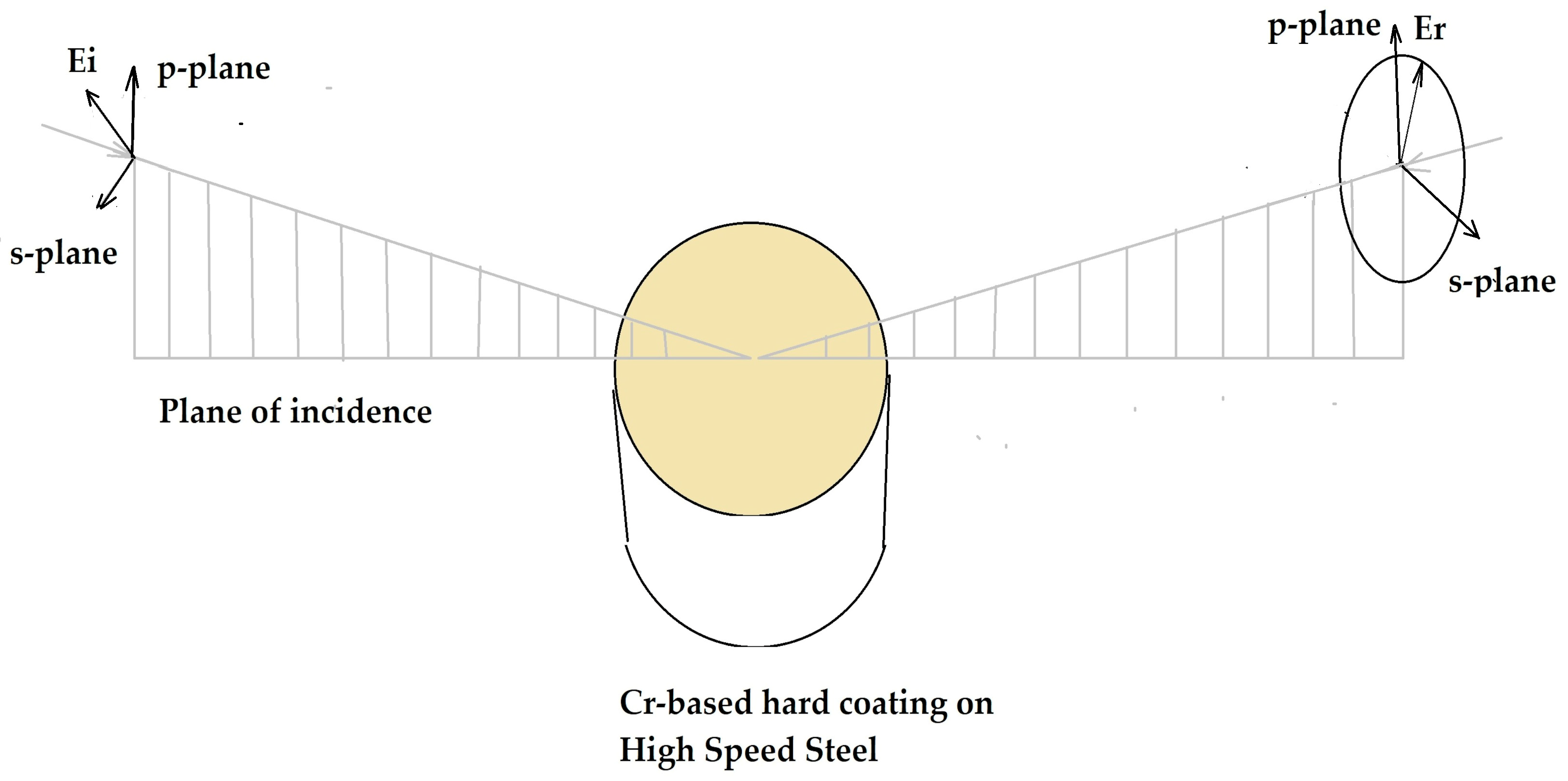
The ellipsometry is based on optical reflectance measurement shown in
Figure 1. The main advantages are the sensitivity and non-destructive measurement of the samples. The method measures the phase change and the ratio of the amplitude of incident and reflected polarised light [
14]. It is used for the characterisation of thin layers. The variation of the composition of different metals and the ratio of metals–nitrogen, the thickness of the different layers, the morphology of the layers, the roughness, etc. all together could change the polarization state of the reflected elliptically polarized light. When the structure of the samples is complex and more layers and physical structures are included, an optical model has to be developed, and fitting procedures have to be performed under regression analysis. This includes the development of a model representing the optical structure of the researched layers—the substrate, the films on the top and the roughness. From the model are predicted Ψ and Δ. The model parameters are varied until the lower error between the model and measured data is reached. The regression analysis finishes with the extraction of the modelled and fitted optical parameters [
15].
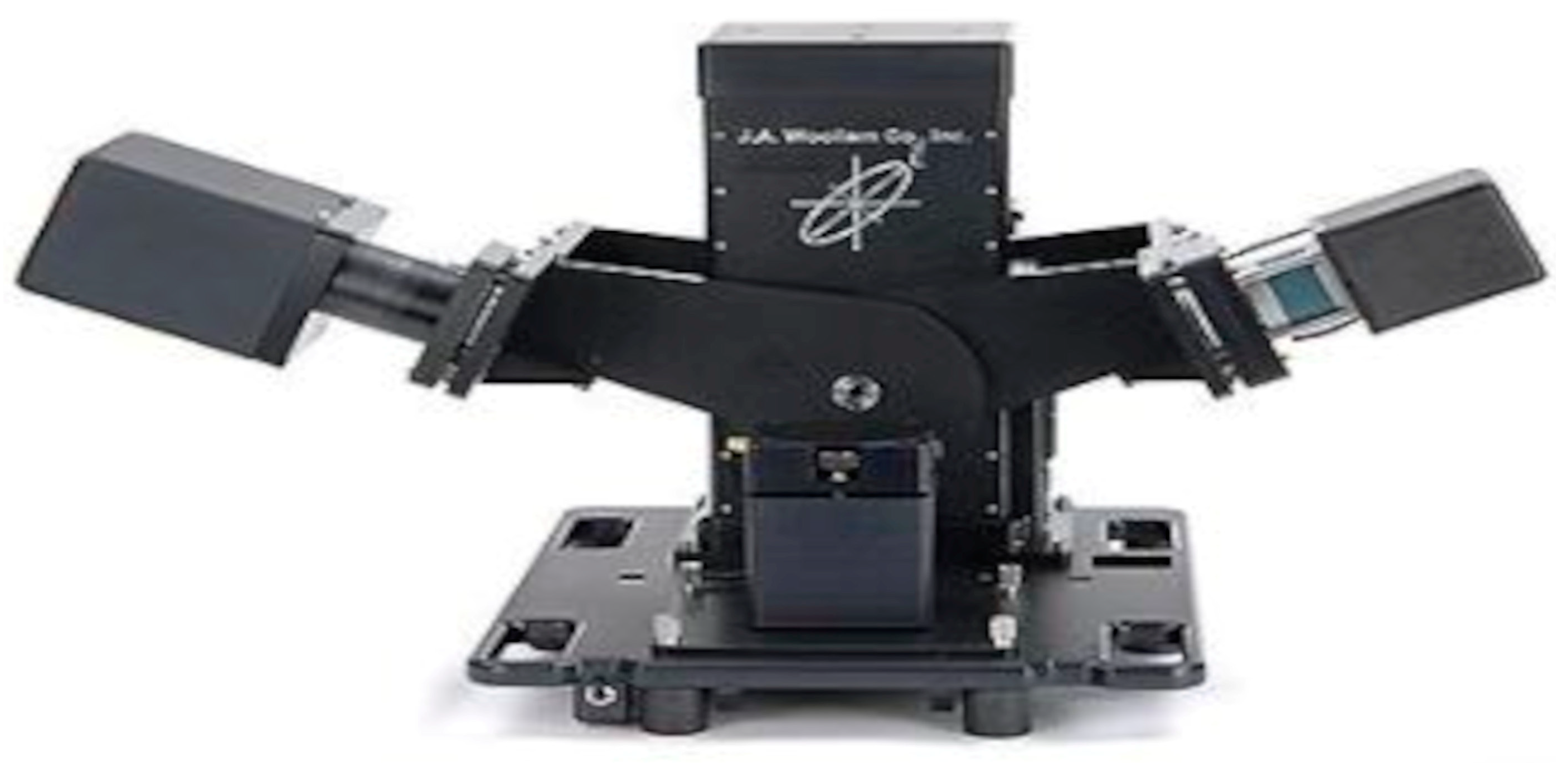
The optical parameters of the coatings were characterised with UV-VIS equipment available at ZONA, Johannes Kepler University (Linz, Austria) shown in
Figure 2. A Woollam ESM-300 Variable Angle Spectroscopic Ellipsometry (VASE, Lincoln, NE, USA,) applied at incident angles of 60°, 65°, 70°, and 75° was used. Data for the frequency-dependent phase difference Δ(ω), amplitude ratio Ψ(ω), and from there, first, the pseudodielectric function < ε
1(ω) + ε
2(ω) >, and secondly, the (physical) real part ε
1(ω) and imaginary part ε
2(ω) of the polycrystalline bulk dielectric function were derived, as well as the corresponding refractive and extinction indexes n(ω) and k(ω). Regression analysis of the complex reflection coefficients obtained was conducted with WVASE© software version 3.686. [
16].
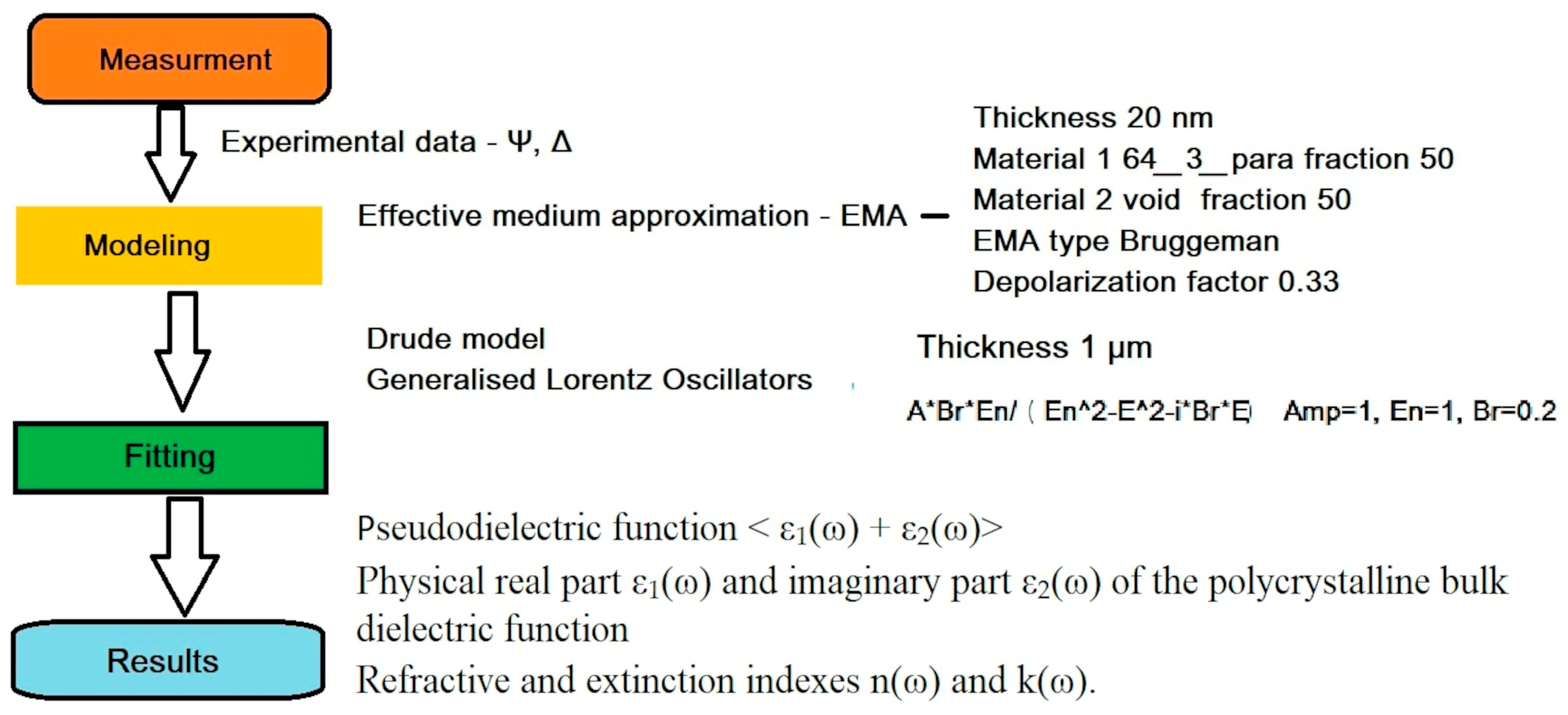
Figure 3 presents the process of regression analysis and the obtaining of optical parameters.
In the software, effective medium approximation (EMA) was chosen to model the effect of the surface roughness [
17] and deduce the polycrystalline bulk dielectric function. Free-carrier absorption was described with the Drude model [
18]. The fitting model of the dielectric function was constructed with generalised Lorentz oscillators [
19]. Supporting characterisation techniques were used for the evaluation of the modelled parameters and the structure and composition properties of the investigated coatings.
The grain size on the coating surface was observed and measured on Hitachi SU 5000 Schottky field emission scanning electron microscope (Hitachi, Japan) in Secondary electron (SE) detecting mode.
A Scanning Electron Microscope (SEM) Zeiss Crossbeam 1540XB (Carl Zeiss NTS GmbH, Germany, Europe) with incorporated Energy Dispersive X-ray Spectroscopy (EDS), (Oxford, UK) was used for the investigation of the surface structure and composition. Focused Ion Beam (FIB) cross sections were used for additional confirmation of the results from coating thickness measurements and to define the size of the different sublayers according to their composition. Subsequently, FIB was used for lamella preparation in order to investigate the morphology of the Cr/CrN/CrTiAlN coating with a JEOL JEM-2200FS (Tokyo 196-8558, Japan) transmission electron microscope (TEM) operated at 200 KeV. This microscope also allows scanning transmission electron microscopy (STEM) and is equipped with an EDS detector X-Max80T from Oxford Instruments (Abingdon, Oxfordshire, UK) for elemental composition identification. The achievable imaging resolution was 0.1 nm (lattice), 0.23 nm (point-to-point), and 0.2 nm (STEM). Atomic Force Microscope (AFM) of Agilent Technologies Inc. (Santa Clara, CA, USA) was used for measurement of coating roughness. X-ray photoelectron spectroscopy (XPS) was also utilised for measuring the composition of the selected samples. The XPS measurements were carried out on an AXIS Supra electron spectrometer (Kratos Analytical Ltd. Manchester, UK) using AlKα radiation with a photon energy of 1486.6 eV. The data evaluation was performed using the commercial data-processing software ESCApeTM version 1.4 from Kratos Analytical Ltd. The energy calibration was performed by normalising the C1s line of adsorbed adventitious hydrocarbons to 284.8 eV. The binding energies (BE) were determined with an accuracy of ±0.1 eV. The concentrations of the different chemical elements (in atomic %) were calculated by normalisation of the areas of deconvoluted photoelectron peaks to their relative sensitivity factors. The sample surface was cleaned by Ar+ ion sputtering (ion energy of 3 eV, sputtering time of 20 min.). The surface composition of this coating was also analysed with JEOL JAMP-9500F Field Emission Auger equipment (Tokyo 196-8558, Japan) with a beam energy of 10 keV. A depth profile was also made through Ar+ sputtering.
3. Results
Nanohardness was compared by reaching the depth of penetration in the sample surface at around 10% of its thickness, corresponding to a load of 10 to 20 mN. Thus, the influence of the substrate nanohardness on the coating hardness could be considered negligible.
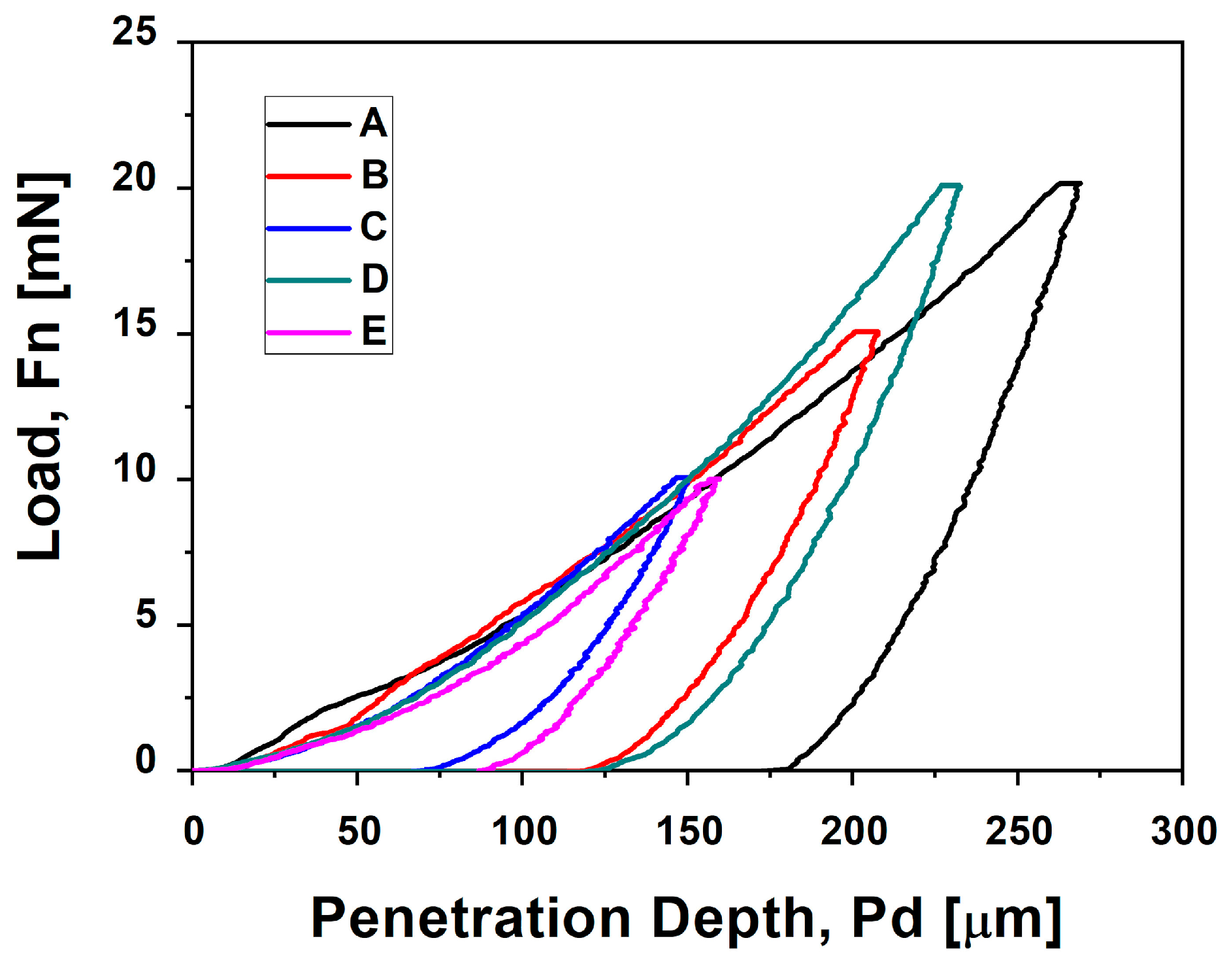
Figure 4 presents the load-displacement curves for the five samples.
Neither the loading nor the unloading part shows any significant pop-ins or pop-outs, implying the absence of cracks. The steepest slope of the loading part is that of the curve of sample C—Cr/CrN/CrAlTiN-1, which corresponds to the highest nanohardness—23.8 GPa.
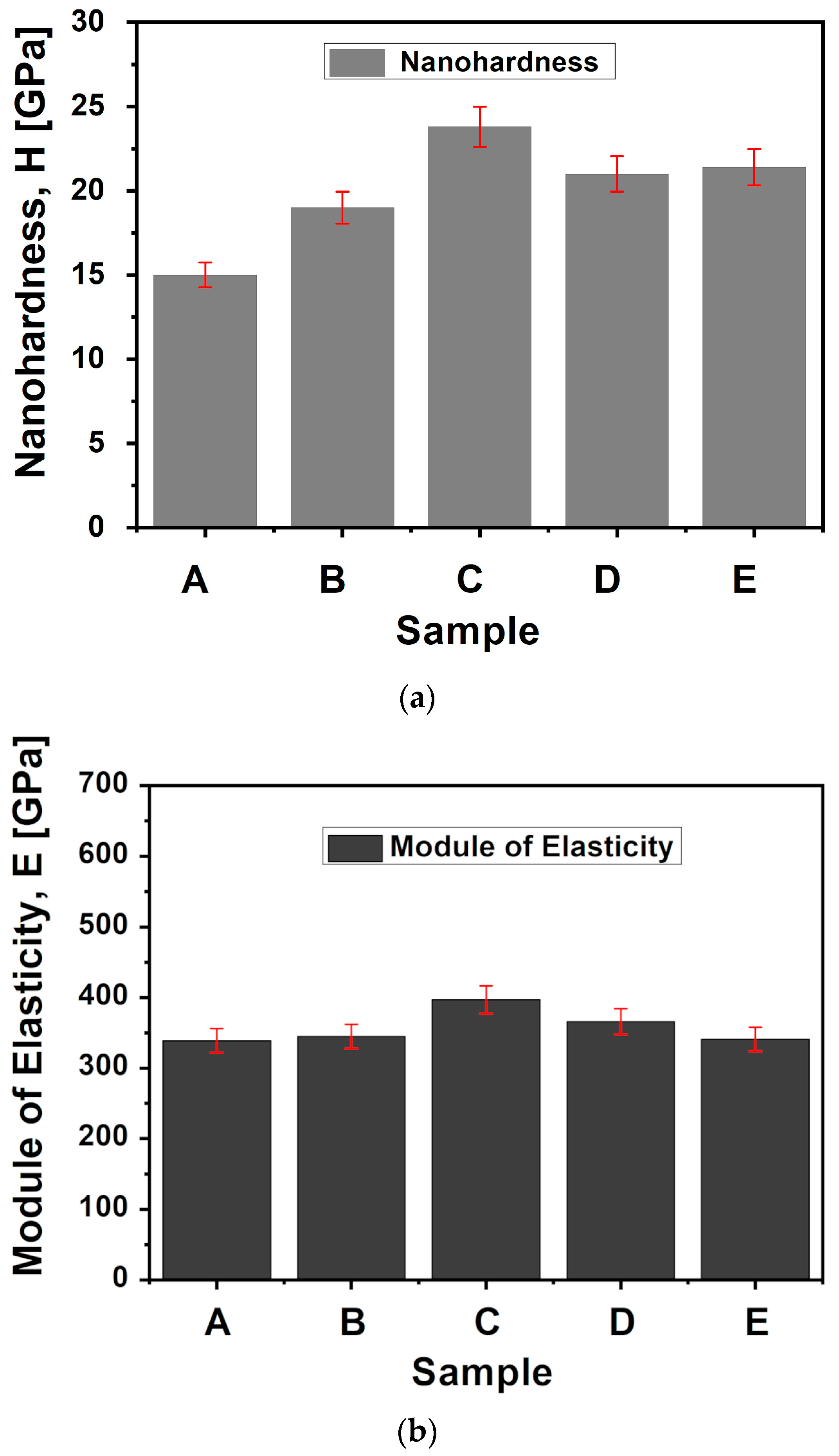
Figure 5 shows the measured nanohardness and modulus of elasticity calculated following the Oliver and Pharr method [
20]. The following expressions are used:
where P
m is the peak load, A is the project area of the contact at the peak load, E and Ei—Young’s modulus for the specimen and the indenter, [GPa], respectively ν and ν
i—Poisson’s ratio for the specimen and the indenter, respectively. The results are generalised in
Table 2.
It could be seen that Sample C—Cr/CrN/CrAlTiN-1 has the highest nanohardness of 23.8 GPa, while the binary CrN sample A—Cr/CrN has, as expected, the lowest nanohardness of 15 GPa. The quaternary structures have higher hardness, followed by the ternary and binary coatings, as also reported in other studies [
21]. The increased hardness of the CrAlN hard coatings, compared to the CrN, is explained by the refinement of the grain sizes, while the improvement of the hardness for the quaternary coatings is attributed to their compact morphology. The trend of the modulus of elasticity is almost similar to the trend of nanohardness. The highest modulus was measured for the quaternary sample C—Cr/CrN/CrAlTiN-1. The discrepancy between the modulus of elasticity and the nanohardness trends, like in Sample E—Cr/CrN/CrAlTiN-2 could be seen due to the fact that both mechanical properties depend on the composition variations. Depending on the Al content, different phases with cubic NaCl structure, wurtzite ZnS and mixed cubic-wurtzite structures contribute to the properties of coatings like TiAlN and CrAlN [
22,
23].
In addition, the Ti/Cr ratio and Al concentration influence the microstructure and properties of the coatings and the corresponding mechanical parameters [
24]. The incorporation of nitrogen also alters the modulus of elasticity [
25,
26,
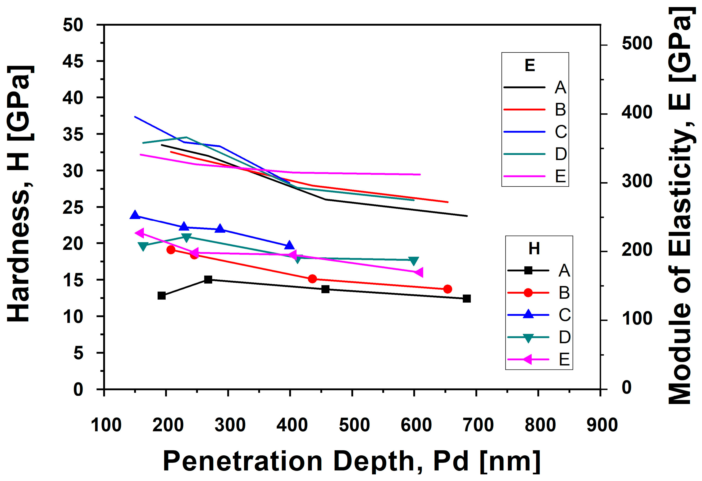
27]. To study how the mechanical properties of substrates affect the hardness and module of elasticity, additional nanoindentation tests were performed as functions of penetration depth. Measurements of hardness and module of elasticity as a function of penetration depth are given in
Figure 6. Researching the samples in-depth, as expected, Cr and CrN sublayers show lower values of both hardness H and modulus of elasticity E than CrAlN, CrTiAlN and CrAlTiN. The slight offset of the curves, even for depths corresponding to the inner layers (Cr and CrN), is due to the differences in the technological regimes during their deposition (current/power of the metal targets and metal/nitrogen ratio) chosen for the concrete technological process. For each of the researched samples, relations between hardness/modulus of elasticity and penetration depth, presented in
Figure 6, look typical for the system hard coating on a soft substrate [
28]. The highest values for both hardness and modulus of elasticity are measured for penetration depth near 10% of the coating thickness, corresponding to coating-only properties. Increasing the penetration depth, the values of the hardness and modulus of elasticity decrease because of the influence of the substrate. The HSS substrates used have a hardness of 10 GPa to 12 GPa. The trends of the curves for the quaternary hard coatings show that their hardness is higher in comparison with the binary and triple coatings in the depths where the properties of the substrate influence the complex hardness. It is expected that they could withstand more load and crack formations and exceed other coatings.
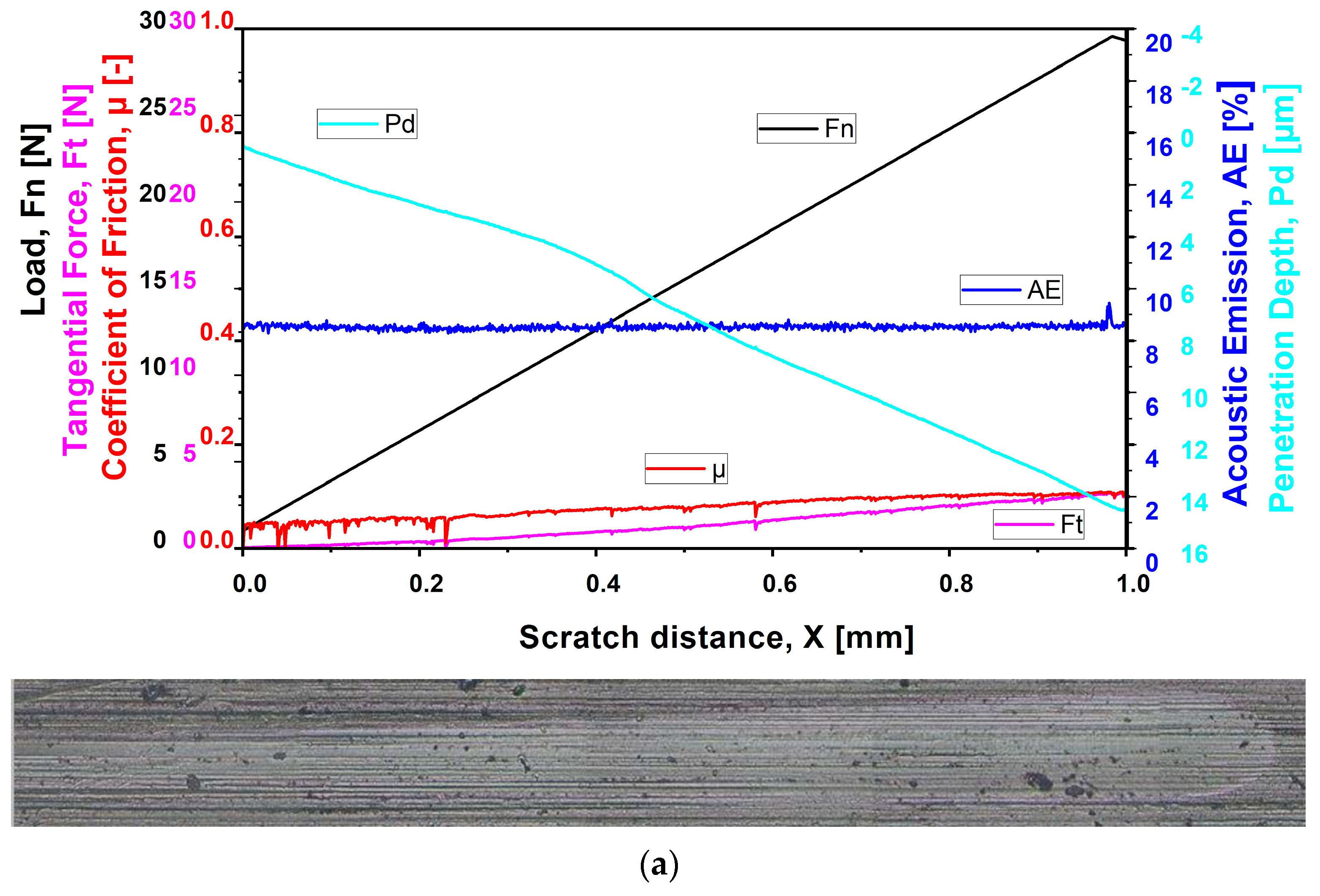
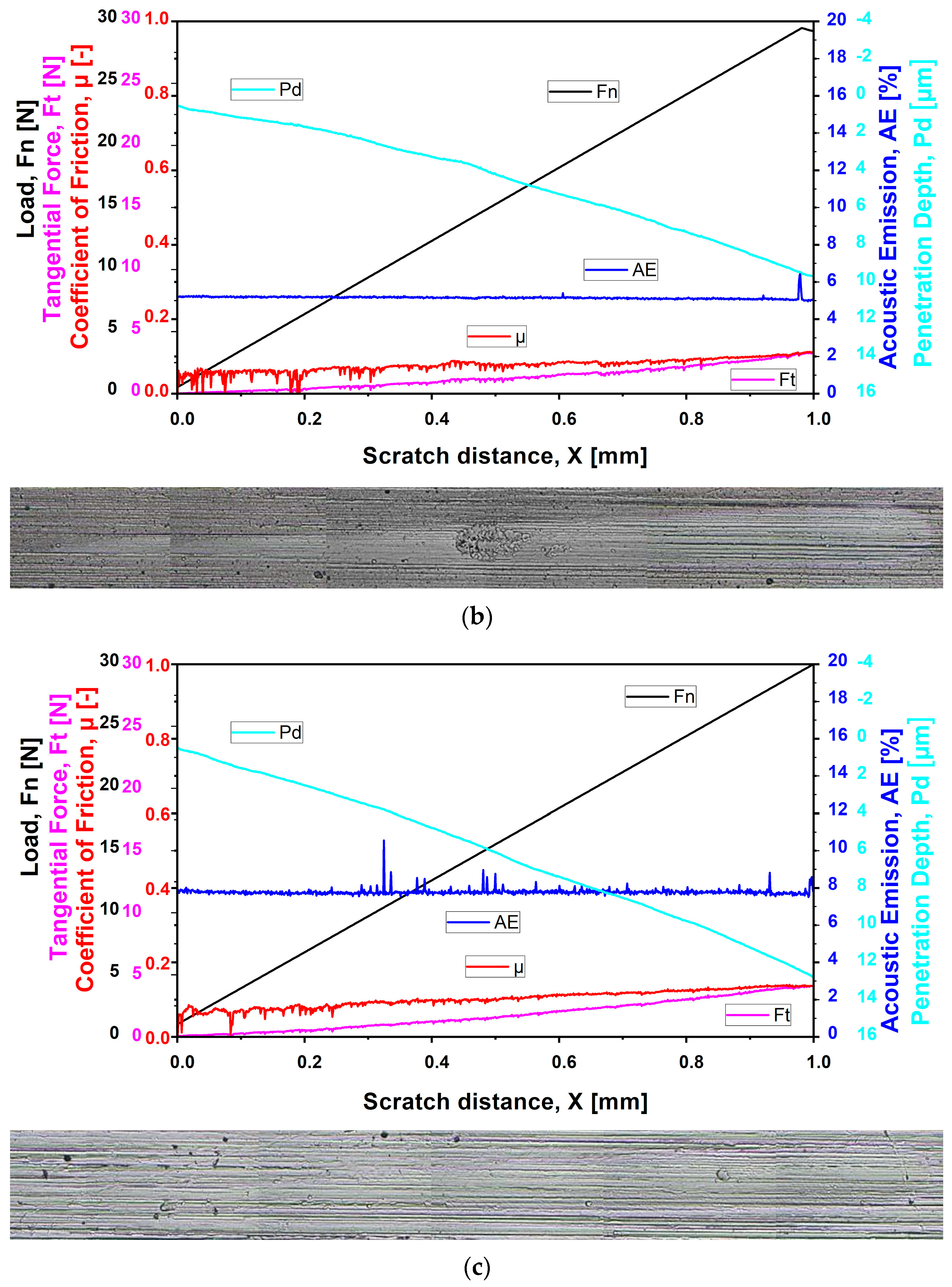
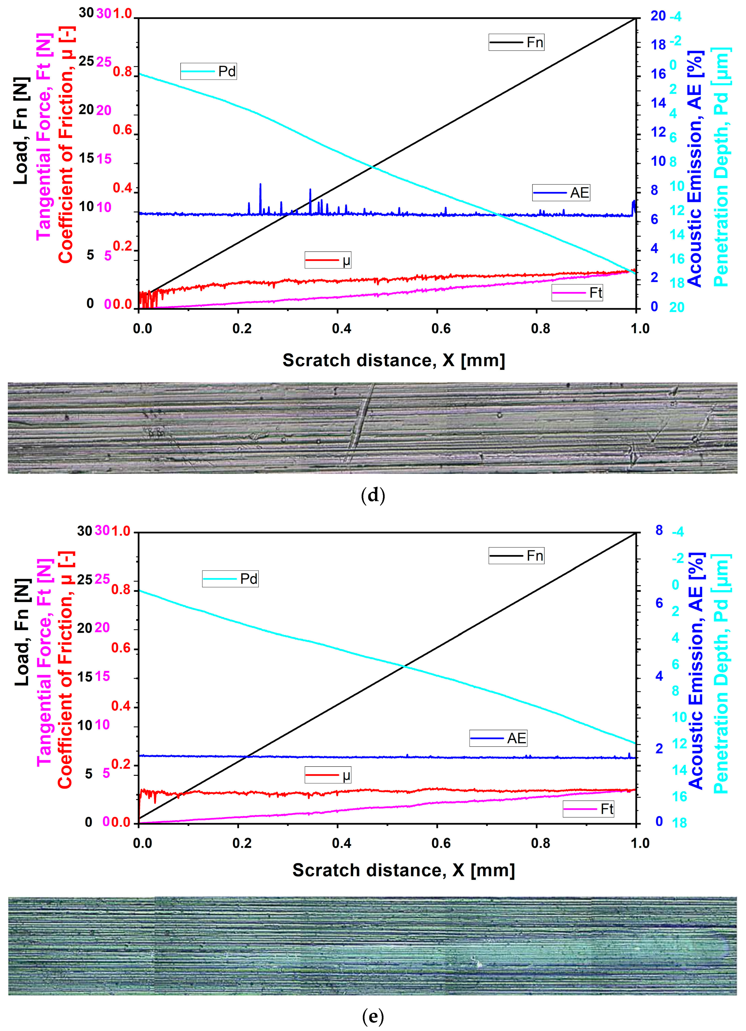
Figure 7 displays the results from the adhesion micro-tests up to 30 N. The trends of normal force F
n [N] (the progressive load during the test), tangential force F
t [N] (the resistance of the material against the indenter), penetration depth P
d [µm] (displacement of the indenter measuring elastic recovery), acoustic emission AE [%] (the noise during the measurement), and coefficient of friction against the diamond indenter µ [-] (determined as the ratio F
t/F
n) [
29,
30,
31] can be seen in different colours on the graphs.
The results show adhesion to the substrate without adhesive failures. The load and friction curves are straight. This is additionally proved by the smooth scratch tracks. The acoustic emission signal (AE) has inessential small fluctuations. The small peak detected in the signal may be due to the roughness of the ground substrates or could be generated by the indenter being lifted at the end of the scratch tests.
In the pictures in
Figure 8, transverse semi-circular cracks are identified for samples A—Cr/CrN and C—Cr/CrN/CrAlTiN-1. Sample D—Cr/CrN/CrTiAlN has lightly seen angular cracks. In samples B—Cr/CrN/CrAlN and E—Cr/CrN/CrAlTiN-2, surface defects have been observed to appear once in each of the scratch tests. It is expected that at higher loads, the samples C—Cr/CrN/CrAlTiN-1, D—Cr/CrN/CrTiAlN and E—Cr/CrN/CrAlTiN-2 will be more resistant to the applied loads because of their hardness.
During the scratch test up to 30 N, no spallation and buckling processes were seen. The absence of cracks in the scratch tract up to loads of 30 N was attributed to the adhesive properties of the transition Cr
xN layers [
32].
The Cr
2N and CrN phases formed Cr
2O
3 on the coating surface, favouring better oxidation and wear-resistant properties that are explained by the denser oxide scales and the different oxide growth modes [
33]. Additionally, the coatings with Al exhibited higher erosion wear resistance over those without Al, such as CrN and TiN. The higher H
3/E
2 ratio and the different wear mechanisms of Al-based coatings were the reason for these characteristics [
34]. The incorporation of Al in the composition of the films produced an increase in the thermal and oxidation resistance that was attributed to the reduction of the CrN crystallite size and formation of the aluminium oxide phase, preventing further crystal growth and oxidation processes [
35].
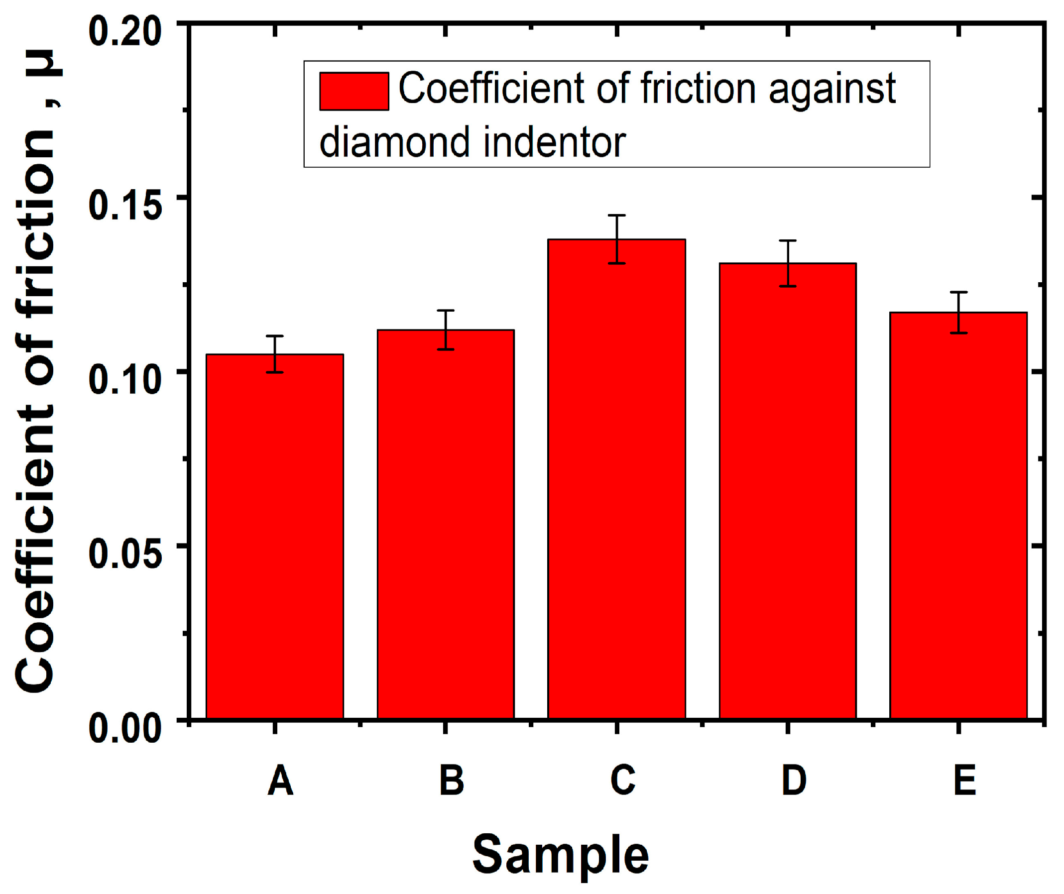
The coefficient of friction for all five samples is shown in
Figure 9. The values generalised in
Table 3 varied between 0.105 and 0.138. The lowest value for the CrN sample in comparison with the CrAlN coatings is also seen, as in other published works, and is explained by the different grain sizes in these layers [
36]. Sample A—Cr/CrN is deposited with a higher flow of nitrogen, supporting the decrease in the grain size of the layers, leading to higher compactness and lower coefficient of friction. The higher coefficient of friction of the coatings with Ti in their structure could be due to the formation of TiO that adversely affects the friction and anti-wear properties of these coatings [
37]. From the quaternary coatings, Sample C-Cr/CrN/CrAlTiN-1, which is deposited at the lowest current of the Ti target, has the highest coefficient of friction. A lower quantity of nitrogen and under-stoichiometric composition could be the reason for this result.
The H/E and H
3/E
2 ratios are used for prediction of fracture toughness of coatings, where H/E represents the elastic strain to failure, and H
3/E
2 represents the resistance to plastic deformation [
38].
Table 4 presents the ratio for the five samples.
The highest elastic strain to failure was calculated for sample D-Cr/CrN/CrTiAlN. This sample also showed the highest resistance to plastic deformation. The value of H/E = 0.1 was accepted as a border value, where layers below this value were forming cracks, and above that value were not [
38]. From the investigated coatings, the quaternary CrTiAlN coating (sample D—Cr/CrN/CrTiAlN) had the highest value of 0.059.
From the investigated mechanical properties, it could be concluded that the coatings are resistant to applied loads up to 30 N and improve the hardness of the substrate in the range of 15 to 24 GPa.
The CrTiAlN coating (sample D—Cr/CrN/CrTiAlN) has an optimal combination of mechanical characteristics. The variations in the deposition process parameters define the structure and composition of the coatings and seriously affect their mechanical properties. The same is expected for their optical properties.
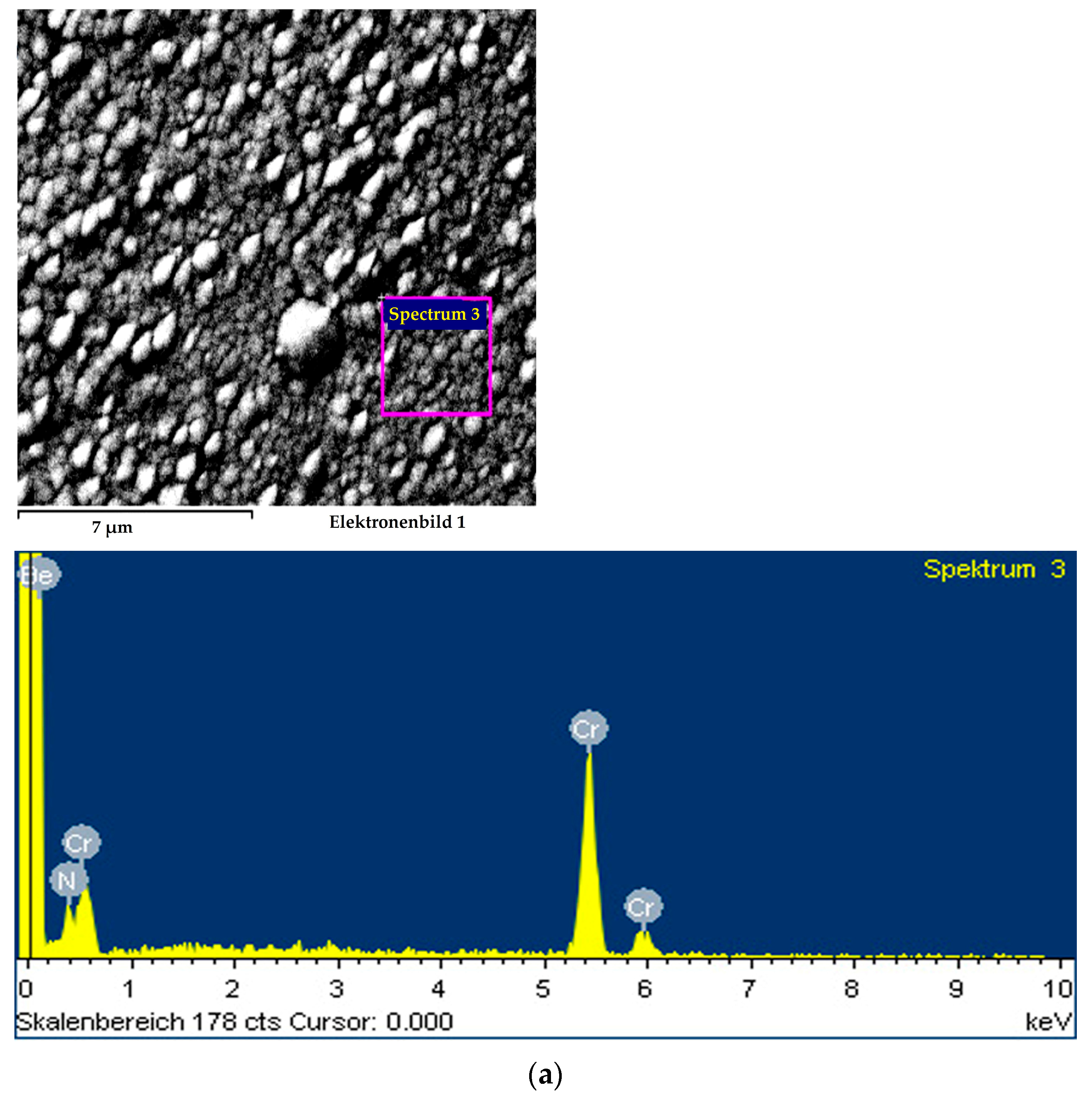
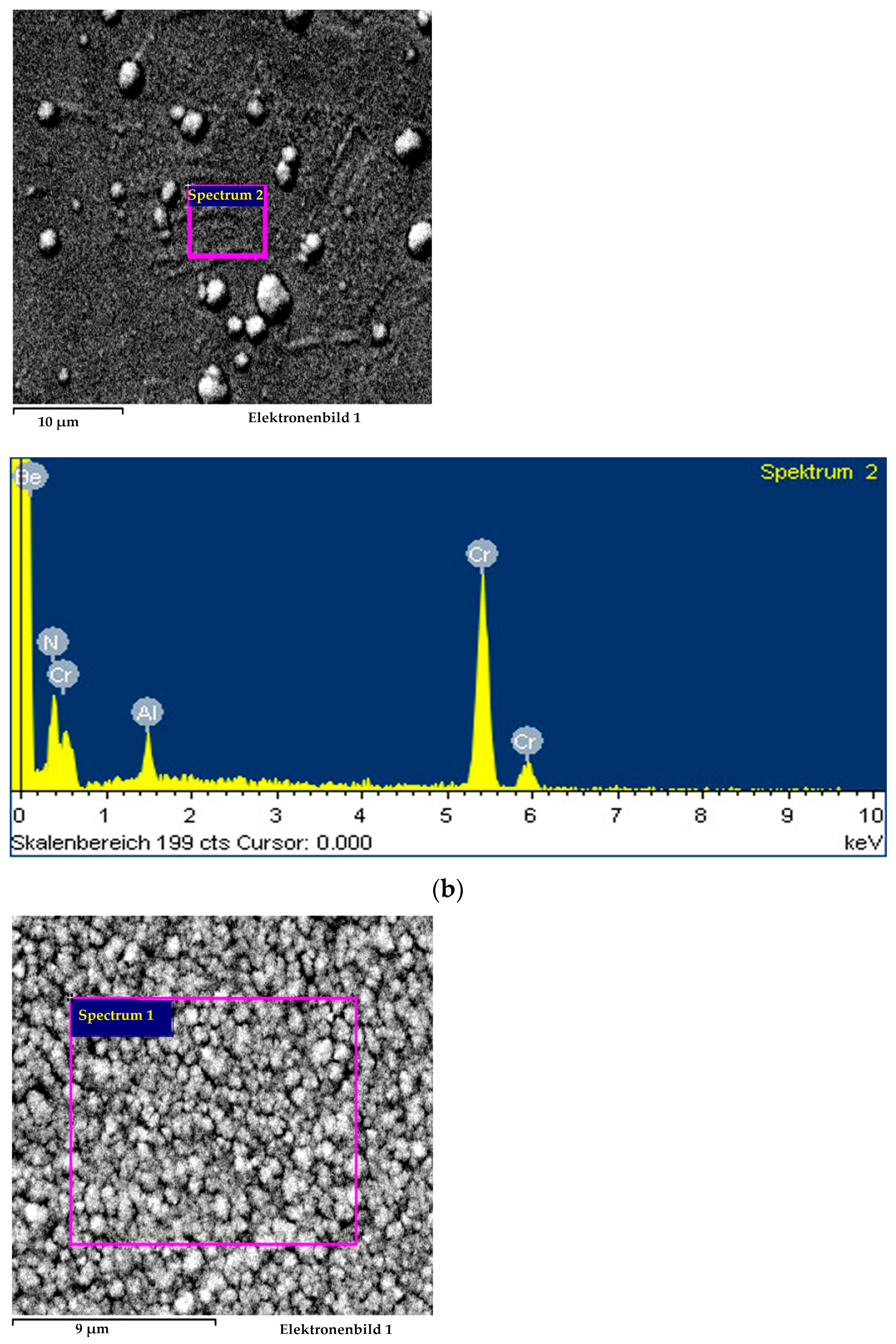
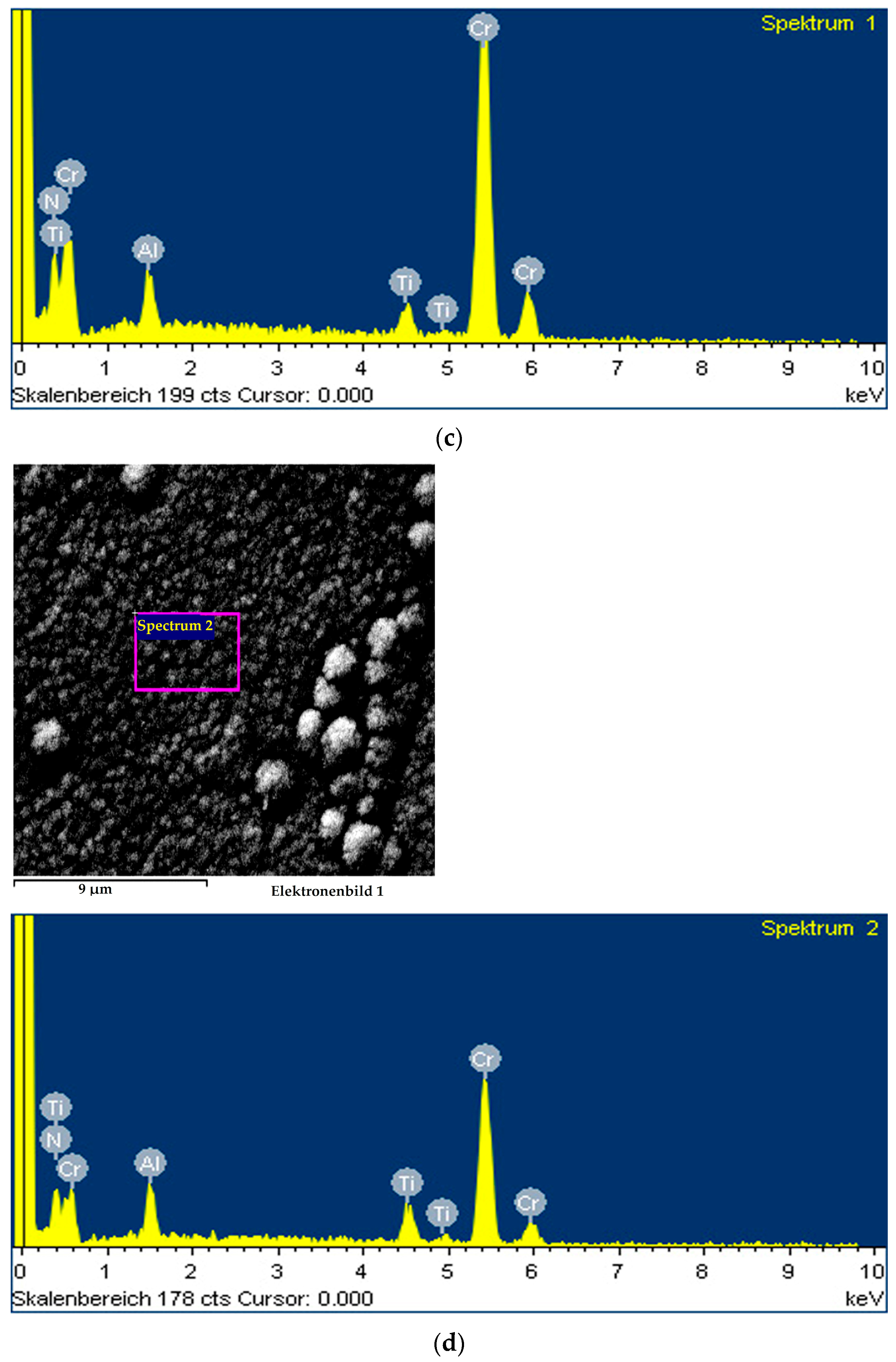
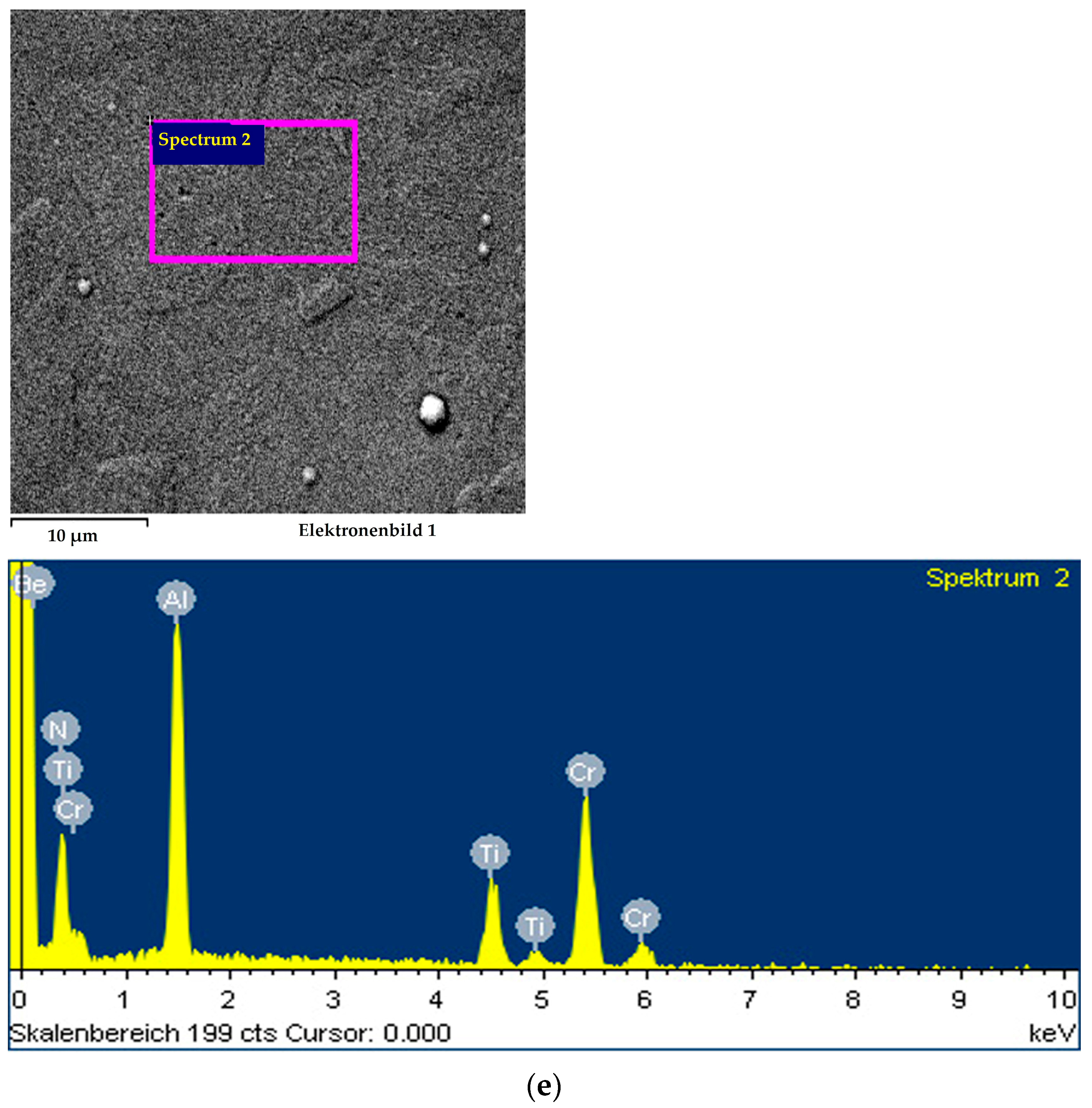
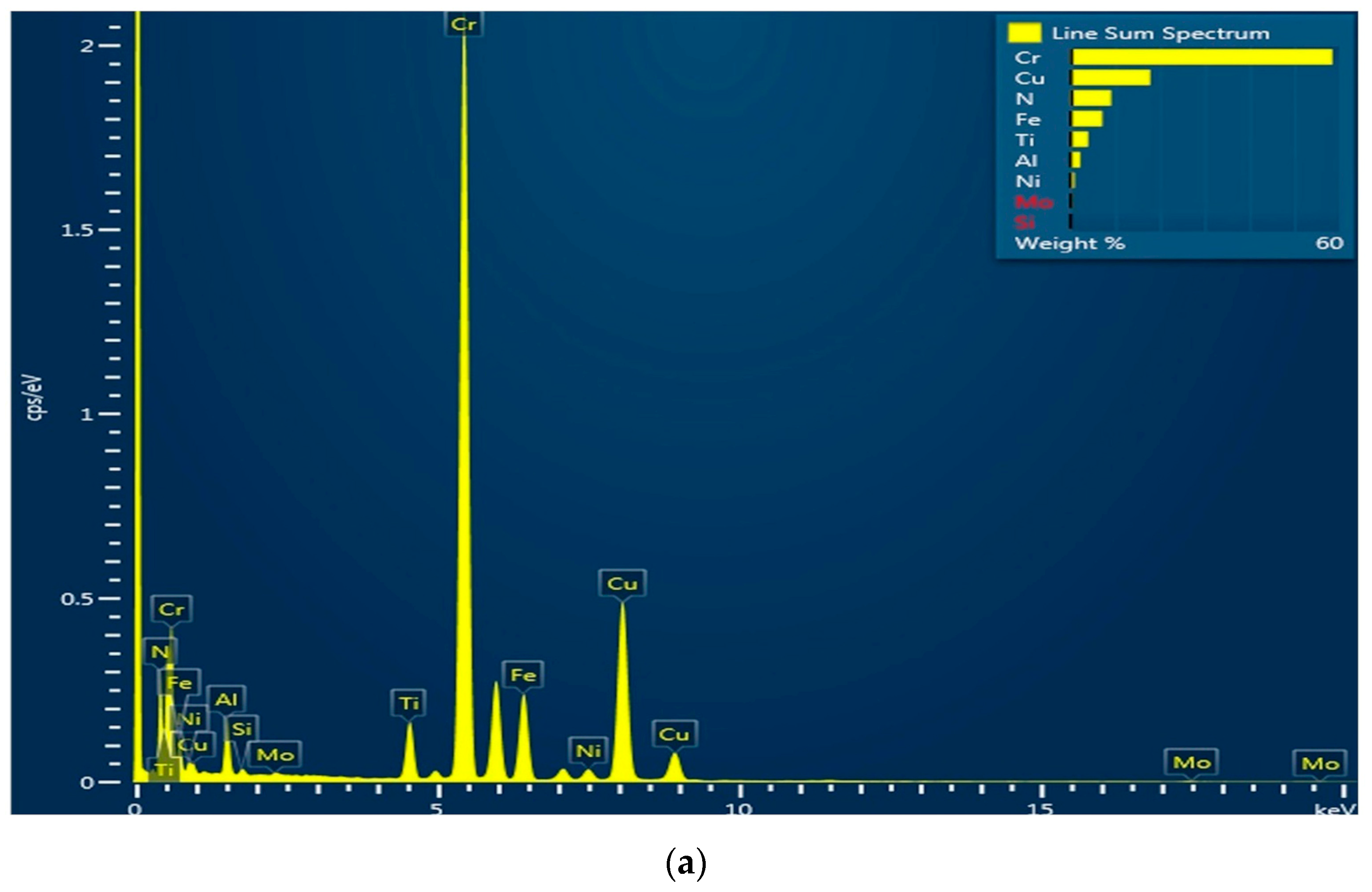
Figure 10 illustrates the results from the SEM surface analysis of the five samples with EDS composition data in
Table 5. The samples have grainier surfaces. In samples B—Cr/CrN/CrAlN and E—Cr/CrN/CrAlTiN-2, where the composition of Al is higher with respect to sample A—Cr/CrN, respectively, samples C—Cr/CrN/CrAlTiN-1 and D—Cr/CrN/CrTiAlN, the surface is dense and smoother. The N concentration value varies greatly due to the difficult quantification of light elements in EDS analysis. However, the results can be interpreted to mean that samples A—Cr/CrN and D—Cr/CrN/CrTiAlN have a higher N content above 50 at. %, while the N concentration in the other samples is below that value. The deposition process parameters in
Table 1 indicate that with a lower current of the Cr target, the percentage of Cr content in the structure also decreases. An increase in Ti and Al in the composition favours the formation of AlN and TiN compounds. They lead to the improved hardness measured in these coatings. The increase in the nitrogen in the quaternary structures (36.6 at. %, 37.9 at. %, 51.0 at. %) corresponds to the improved coefficient of friction (0.138, 0.131, 0.117). The decrease in the metal Cr/Ti (18.86, 7.03, 2.9) and Cr/Al (15.67, 7.24, 1.17) ratio also could support these results. The module of elasticity decreased and followed this trend.
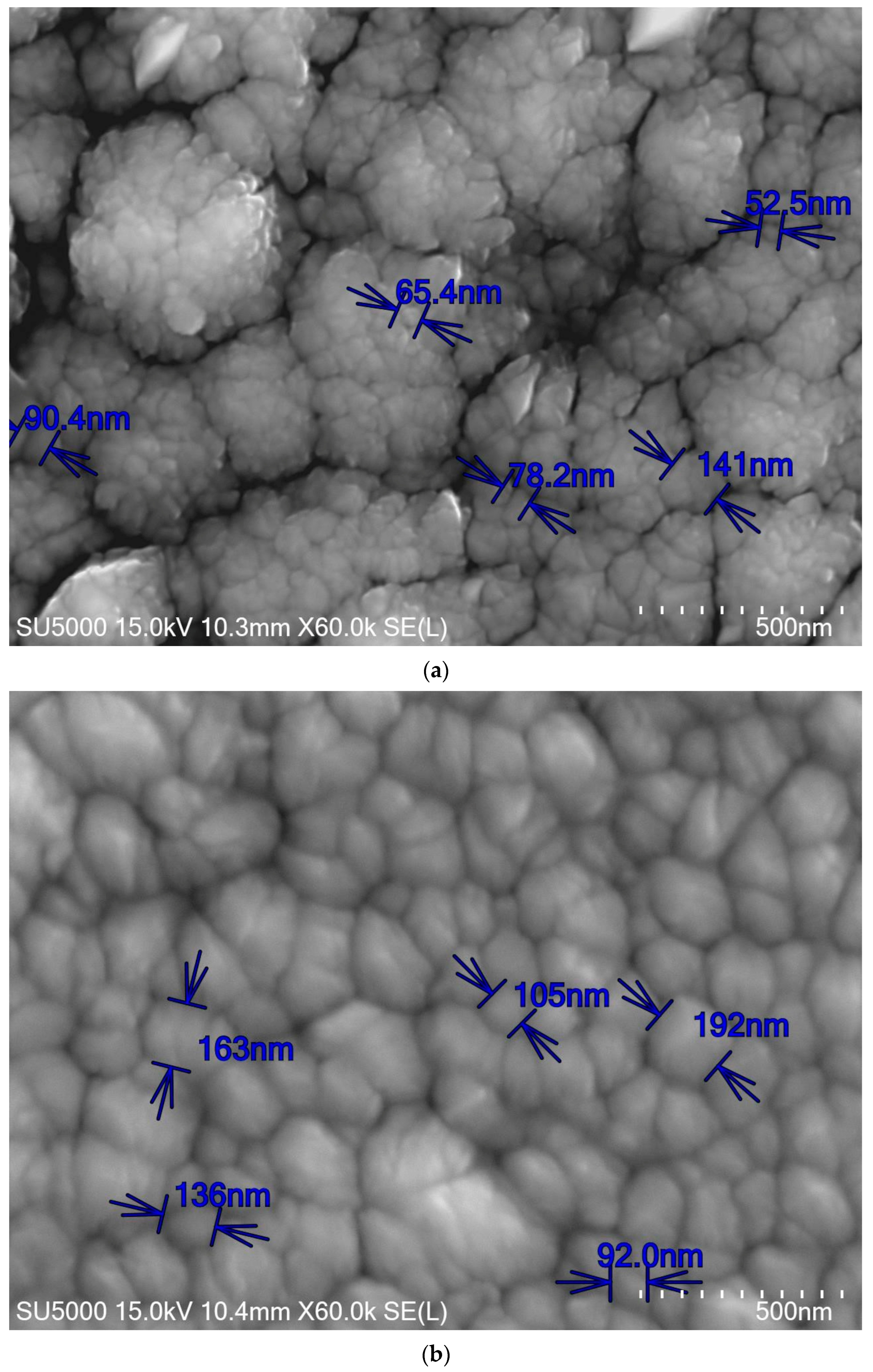
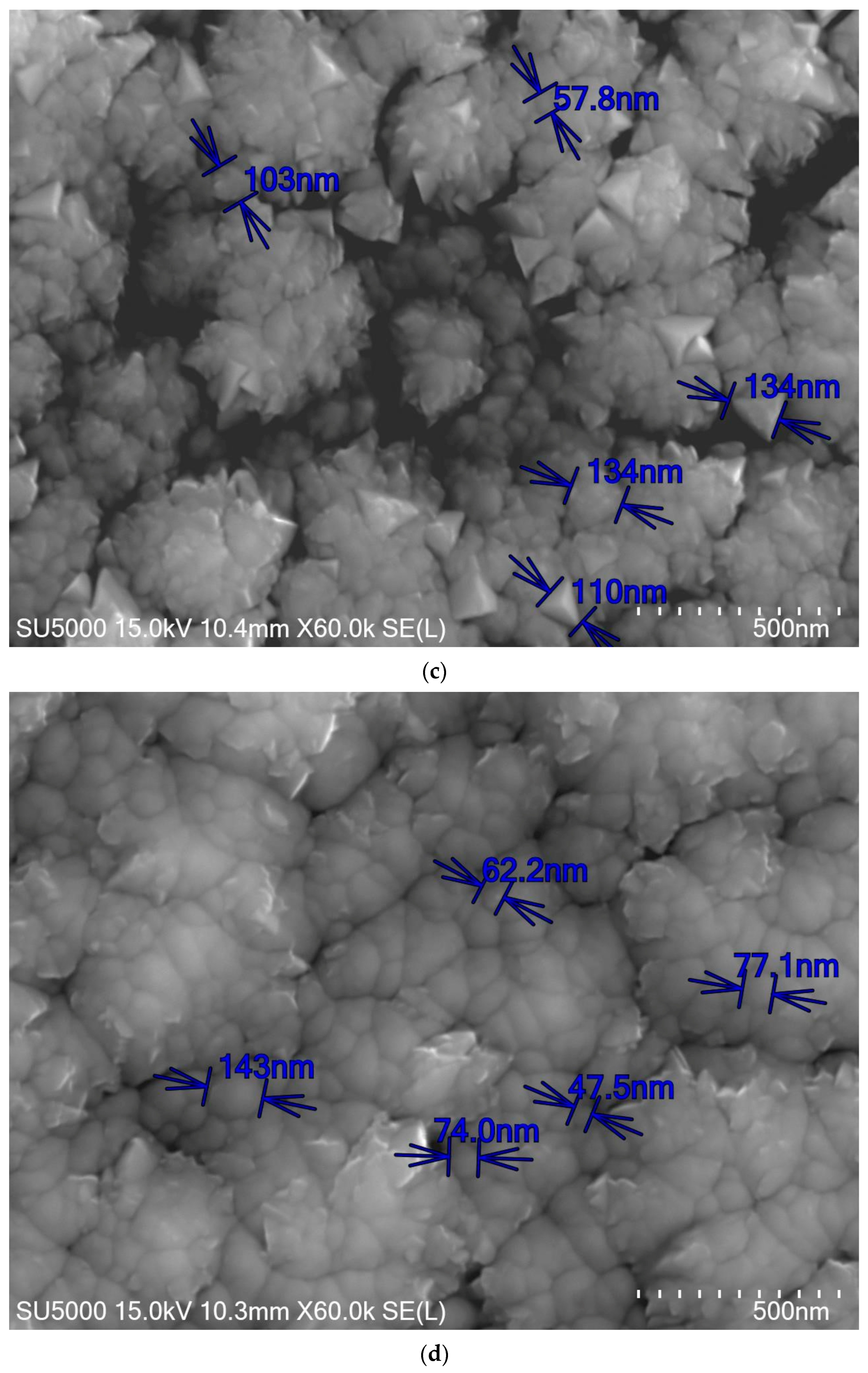
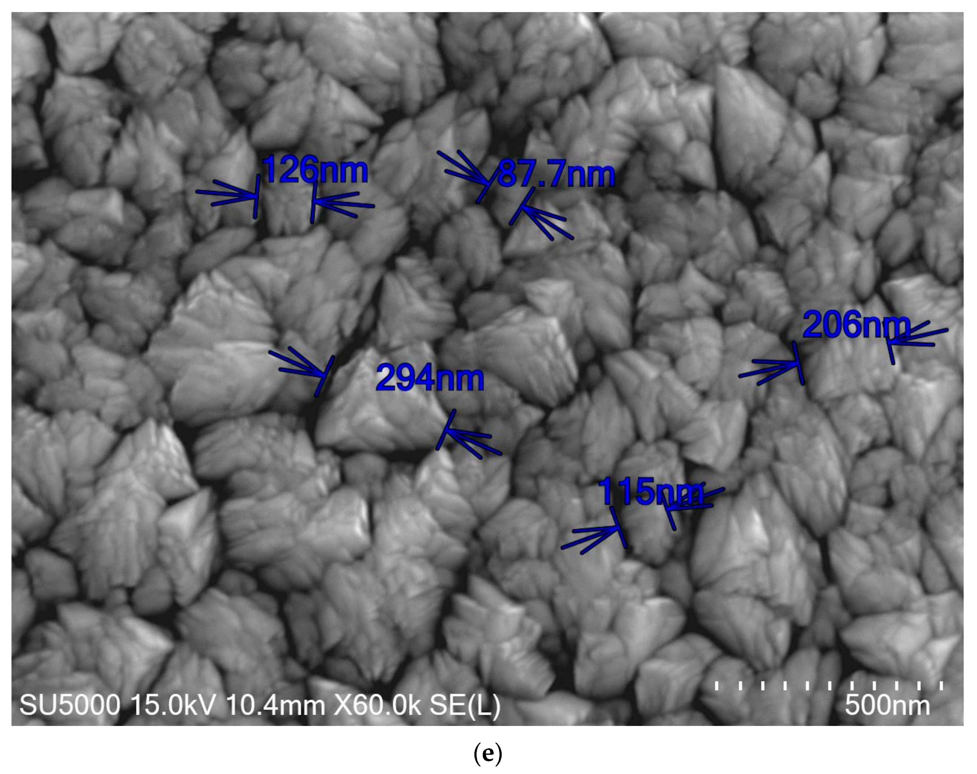
The results for grain size are shown in
Figure 11, and the average size of the grains is summarised in
Table 6. Samples D—Cr/CrN/CrTiAlN and A—Cr/CrN have the lowest average grain size of 80.8 nm and 85.5 nm. Sample C—Cr/CrN/CrAlTiN-1 has an average grain size of 107.8 nm. Samples B—Cr/CrN and E—Cr/CrN/CrAlTiN-2 have large average grain sizes of 137.6 nm and 165.7 nm. The mechanical properties of the layers depend on the grain size. The module of elasticity decreases with the size of grains as it is in the comparison of couples of samples A—Cr/CrN–B—Cr/CrN/CrAlN and C—Cr/CrN/CrAlTiN-1–D—Cr/CrN/CrTiAlN. In other cases, there is an opposite dependence as it is in the comparison of sample E—Cr/CrN/CrAlTiN-2 with D—Cr/CrN/CrTiAlN and C—Cr/CrN/CrAlTiN-1. For grain size with bigger dimensions, other factors influence elasticity, like porosity, grain boundaries, and atomic distances [
39]. Hall-Petch effect is also seen for sample D—Cr/CrN/CrTiAlN, where the lower grain size led to higher yield strength and hardness. This sample showed the highest elastic strain to failure and resistance to plastic deformation and is expected to be appropriate for applications requiring improved fracture toughness properties. The smaller grain size of sample D—Cr/CrN/CrTiAlN is also the reason for the lack of defects during the scratch performed to a load of 30 N.
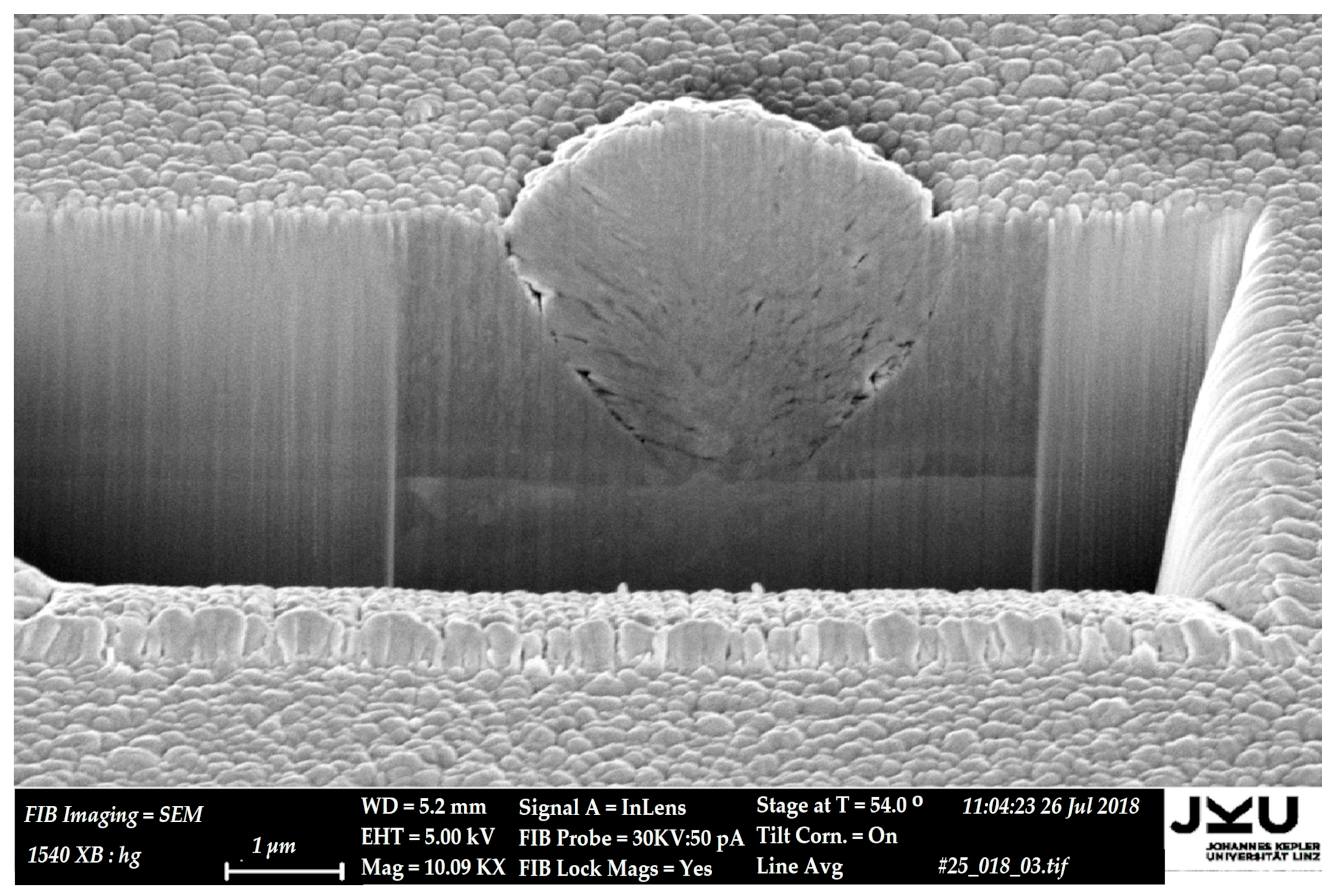
There are other factors besides the chemical composition, which influence the optical properties. The thickness of the layers is very significant. Defined cross sections were made with the FIB in order to determine the thickness of different sublayers and coating structure as a total. Different sublayers could be distinguished by contrasting differences due to the different compositions. The FIB cut of Sample C—Cr/CrN/CrAlN is presented in
Figure 12 and all data are summarised in
Table 7.
In
Figure 13, one can see the typical column structure for Cr-based coatings. Defects could be formed in the layers during the deposition of PVD hard coatings, especially at lower temperatures. The defects from the other side change the optical properties and could lead to errors in the analysis of the results. In the researched coatings, the defect starts from the substrate and propagates through the coating, indicating the substrate as a source for the occurrence of defects, not the technological regimes. Having shown the best combination of mechanical characteristics (hardness, adhesion, coefficient of friction and elastic strain to failure and resistance to plastic deformation) for low-temperature and lubricant-free industrial applications on tools and devices, sample D—Cr/CrN/CrTiAlN was chosen for further composition and morphology characterisation via TEM analysis.
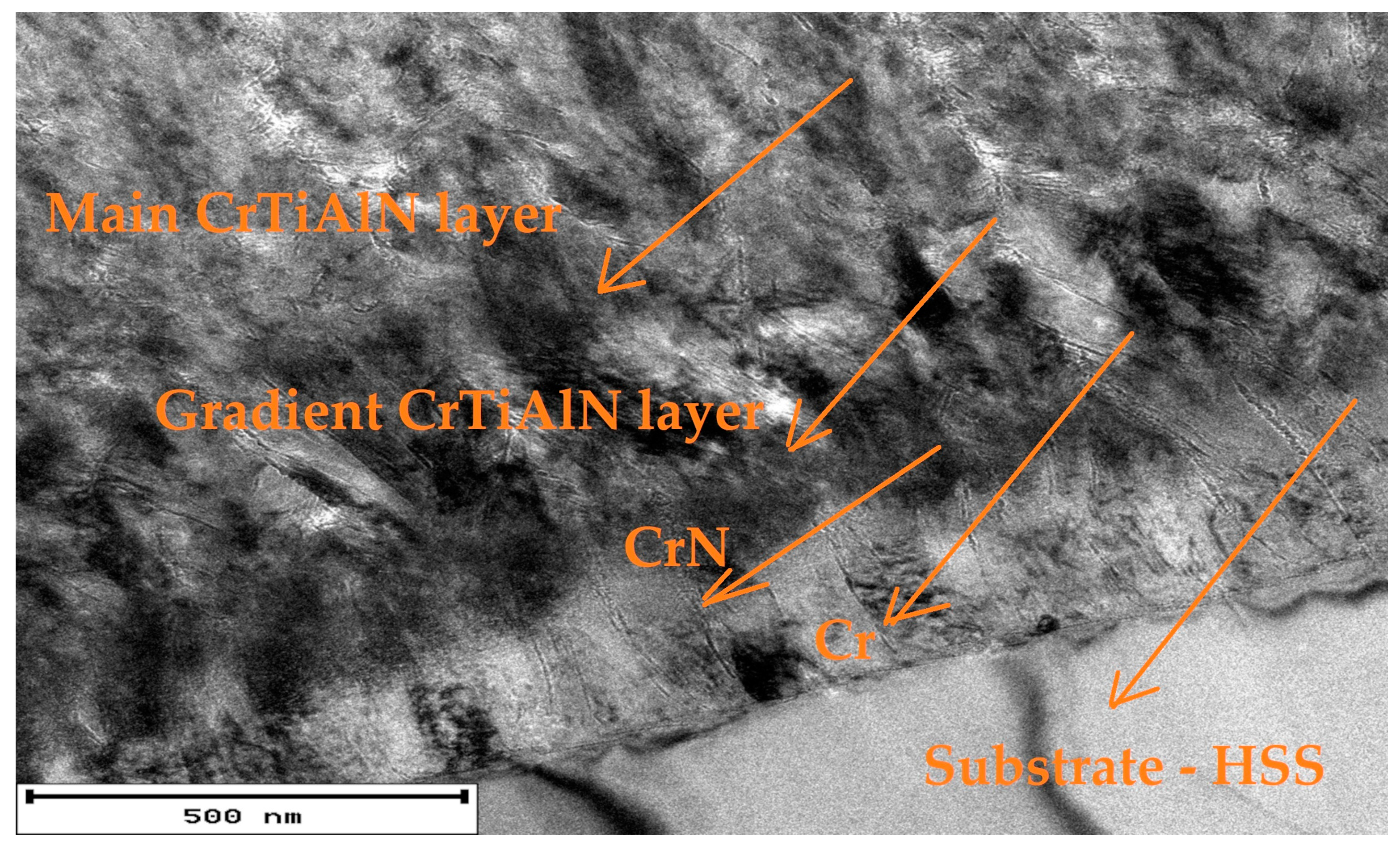
During the deposition of the coatings, transition layers are used with different chemical compositions. Their purpose is to realise a smooth transition between the adhesion layer and the coating. They are deposited with a gradient to have reliable adhesion between the main and the adhesive layer and the substrate. It is expecting the optical properties to be influenced by these layers. TEM analysis was used to investigate the sublayers.
The high-resolution phase-contrast image in
Figure 14 visualises the different sublayers of the coating, starting with the HSS substrate in the right bottom corner of the image—the adhesion Cr layer, the transition CrN layer, and the main CrTiAlN layer.
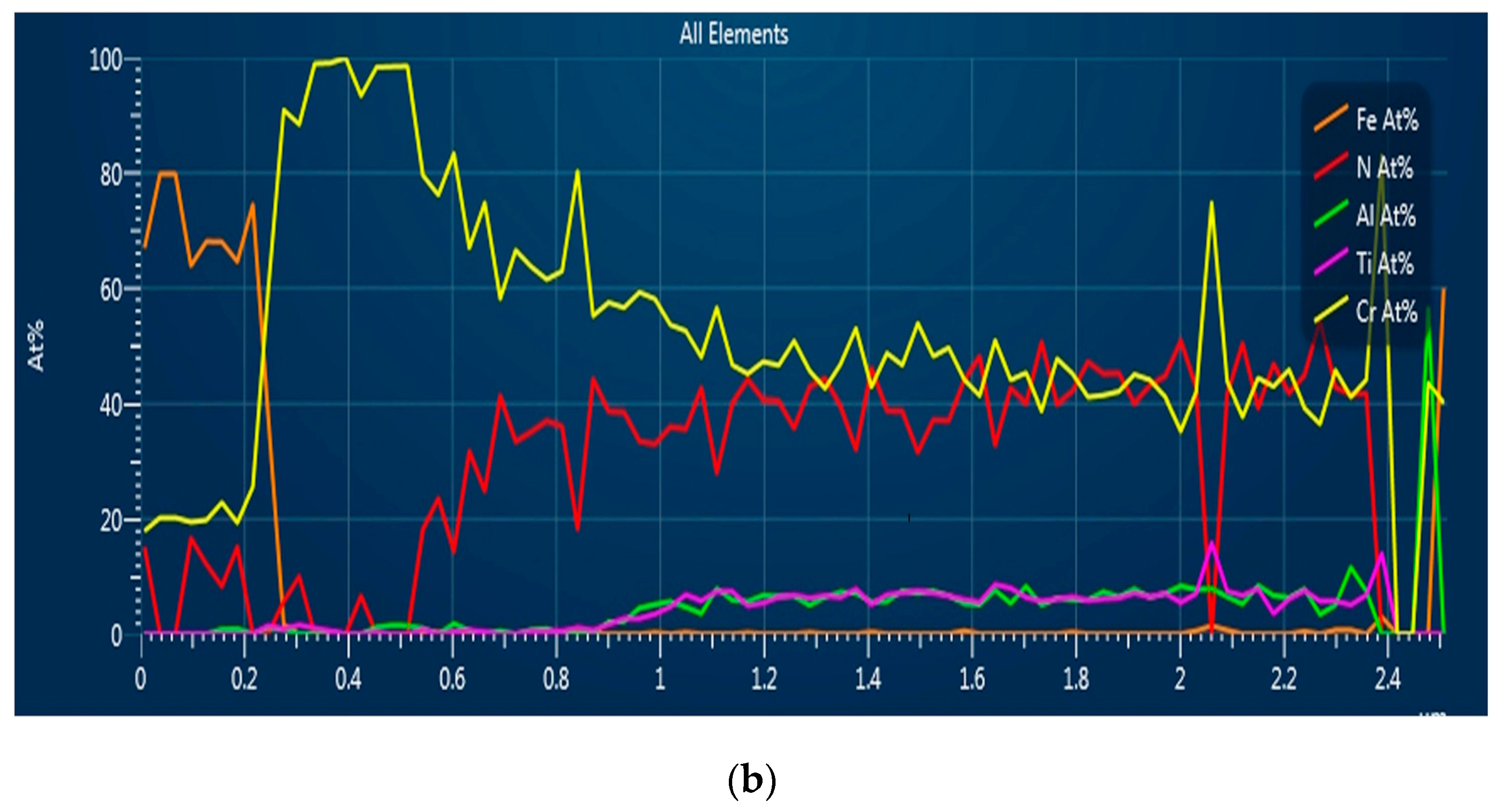
STEM, in combination with EDS, was used for determining the composition across the layer system. The results are presented in
Figure 15. At the beginning of the line scan, the result reveals the Fe of the substrate. Next, the Cr content increases up to 100%, indicating the adhesion of the Cr layer. This is followed by the nitrogen increasing up to 38% and a decrease in Cr to about 40%. After the transition of the CrN layer, Ti and Al are increasing almost equally to 8%, indicating the main CrTiAlN layer.
The gradient transition of the chemical composition from the Cr/CrN sublayers to the main CrTiAlN layer is the reason for the improved cohesion of this coating.
Through the characterisation of bonding states by XPS, it is possible to elucidate what is prepared by the deposition technology chemical compounds. It is very important to know how the method (instrument) works. The bonding states are key factors in realising this goal because they are sure signs of their presence. If the chemical compounds in the coating are known, a reasonable conclusion about its phase composition could be made.
XPS analysis was performed to determine the compounds composed of the coating for sample D—Cr/CrN/CrTiAlN. The element concentrations after surface cleaning by Ar
+ ions are shown in
Table 8. It is seen that oxygen and carbon concentration was under 10 at. % implying that they are attributed to the very near surface layers of the coating. The latter is usual for such types of nitride coatings [
40].
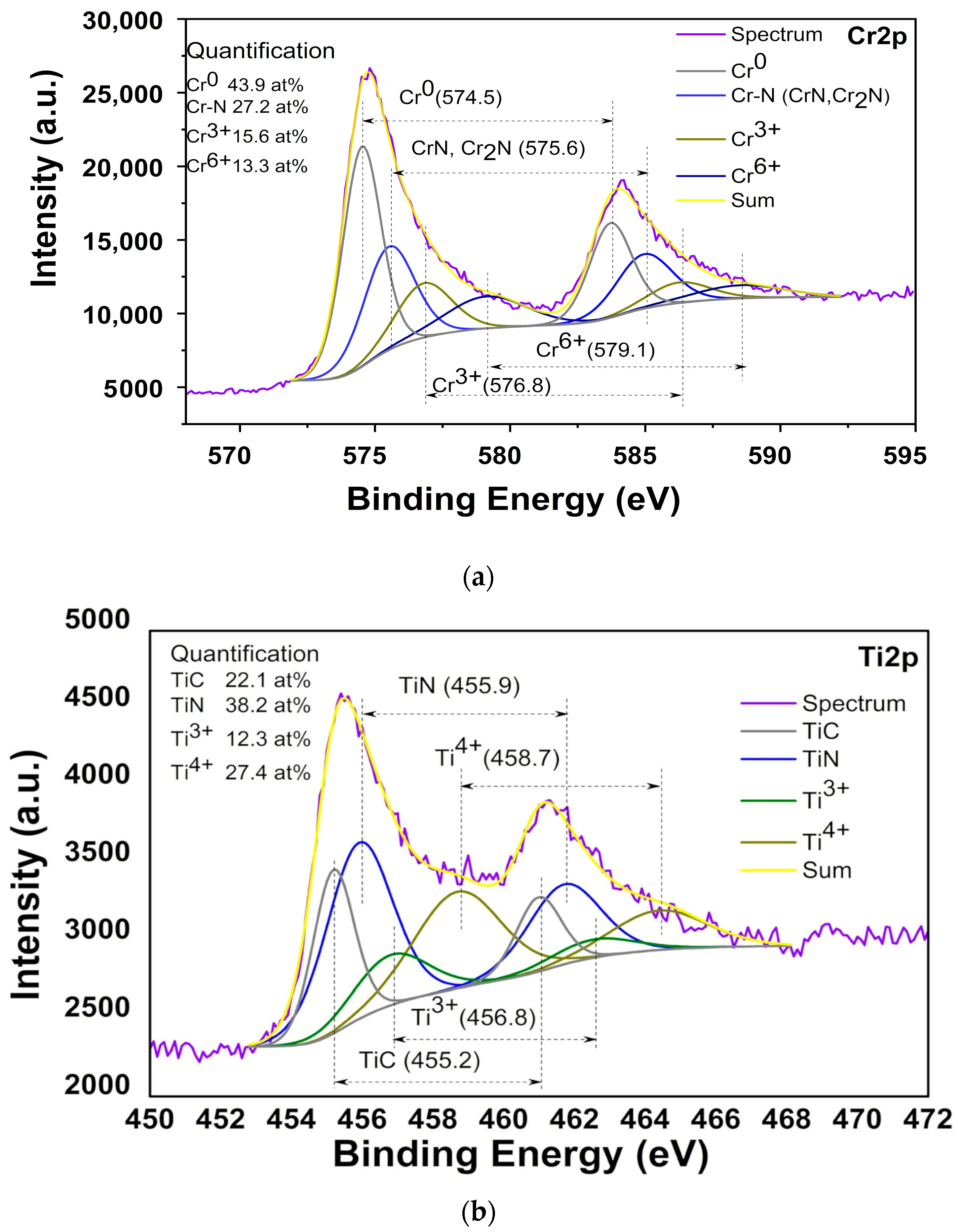
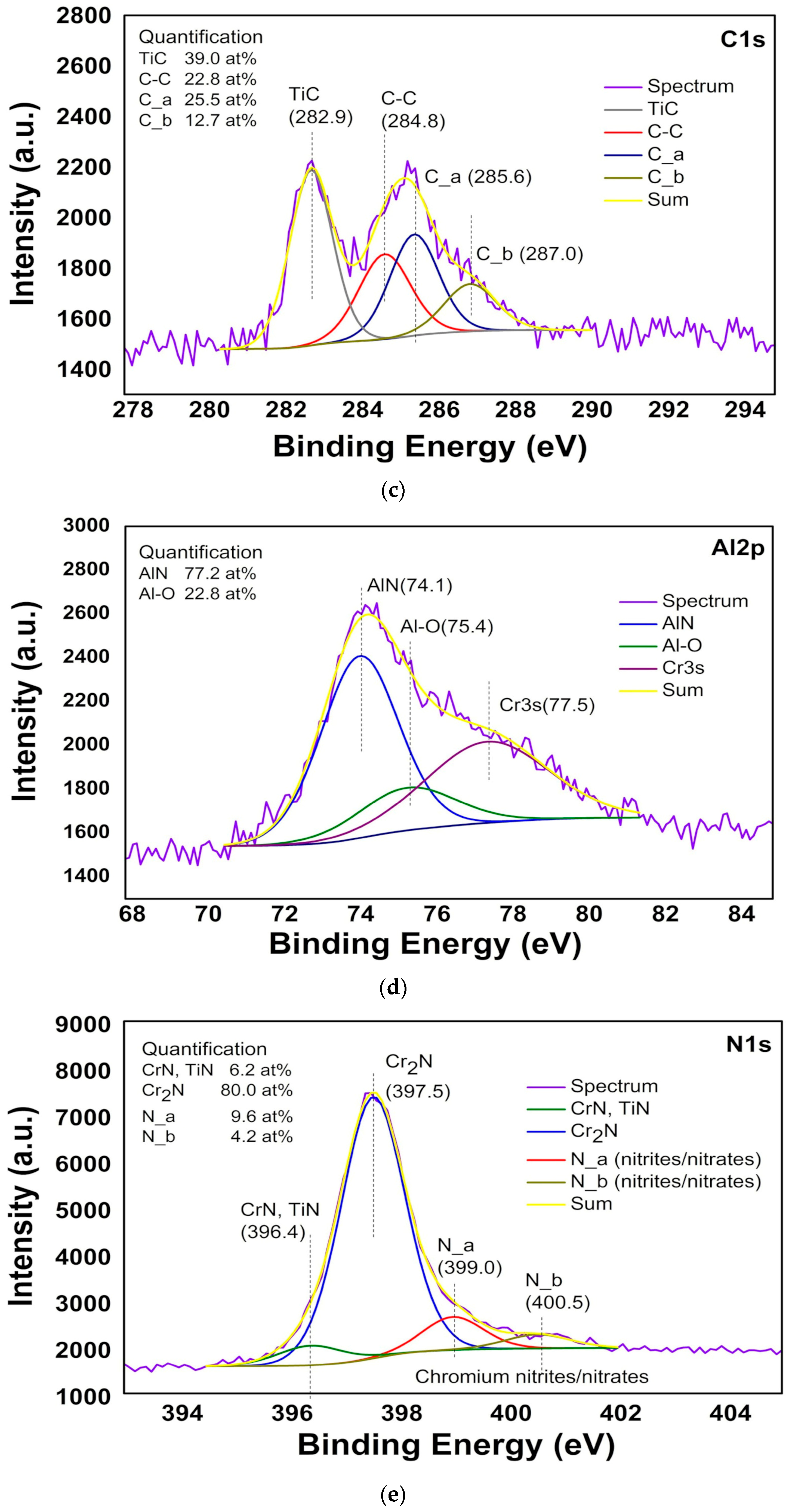
High-resolution photoelectron spectra of Cr2p, Ti2p, Al2p, N1s, and C1s taken after the surface treatment are presented in
Figure 16. The spectra were deconvoluted, and all peaks were assigned to different chemical states according to reference data. In the Cr2p region (
Figure 16a), a doublet of peaks centred at ~575 and ~584 eV was observed, corresponding to Cr2p
3/2 and Cr2p
1/2, respectively. The spectrum deconvolution revealed four components with different values of binding energies, corresponding to different chemical states of Cr: metallic chromium Cr
0 (574.5 eV), nitride compound CrN/Cr
2N (575.6 eV), oxide or hydroxide Cr
3+ (576.8 eV) [
34], and Cr
6+ (579.1 eV) [
41]. Chromium in a metal state is the prevailing part of 43 at. %, while the nitrides compose 27.2 at. %. Both chromium oxides and hydroxides are less than 30 at. % in the coating composition. The Ti2p spectrum consists of four components assigned to TiC (455.2eV), TiN (455.9eV), Ti
3+ (456.8 eV) and Ti
4+ (458.7 eV) [
42]. The main component is TiN, which represents 38.2 at. % of the Ti2p peak. The presence of TiC was confirmed by the peak at 282.9 eV BE observed in the C1s spectrum and characteristic of TiC [
42,
43,
44]. The peak at BE of 284.4 eV corresponds to C-C bonds (284.8 eV), while the other peaks indicate different groups absorbed on the surface, like (C-O, C=O, C-N) [
42,
43,
44,
45,
46]. The deconvolution of the Al2p spectrum is presented in
Figure 16d. It should be noted that the deconvolution was performed taking into account the overlapping of the Al2p and Cr3s peaks. The peak quantified at 77.20 at. % and positioned at 74.1 eV, BE was assigned to AlN. The two peaks at 75.4 eV and 77.5 eV were identified as an Al-O bond and Cr3s [
47,
48]. The deconvolution of the N1s (
Figure 16e) revealed four peaks related to nitrides in different states. The main peak comprises 80 at. % of the total quantity of nitrogen. The binding energy maximum is positioned at BE of 397.5 eV, which is associated with nitrogen in the Cr
2N compound [
40]. The peak at 396.4 eV corresponds to CrN and TiN. The peaks at higher binding energy, 399.4 eV and 400.5 eV, could be explained by the existence of chromium nitrides/nitrates as well as a bond of nitrogen–carbon [
34,
36]. The XPS analysis has revealed that the studied coating consists predominantly of transition metal nitrides such as Cr
2N, CrN, TiN, and AlN. A considerable quantity of chromium in a metal state was found as well.
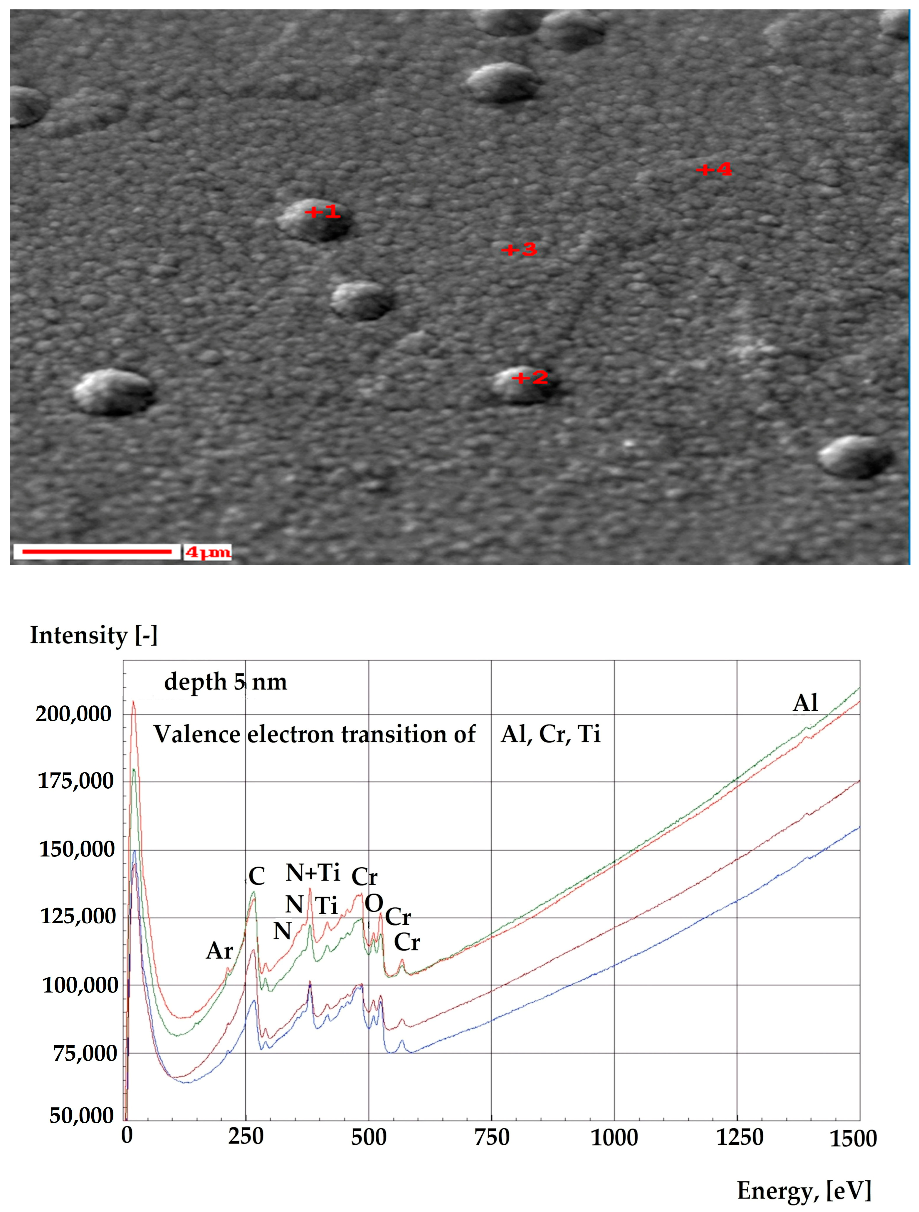
Auger electron spectroscopy (AES) was used for sample D— Cr/CrN/CrTiAlN; it was chosen because of the presented optimal mechanical parameters. The goal was to understand if there were deviations in the properties of the coatings on the surface and in depth, for if there were unexpected deviations, they could bring different optical properties in the same technological sample. Firstly, a surface analysis was made in four points (marked in red) on sample D—Cr/CrN/CrTiAlN. In all points, the composition of the coating was the same as shown in
Figure 17. Next, a depth profile was performed by sputtering, and no differences in the chemical composition of the coating were revealed.”
From the compositional and morphological analysis of the results, it can be concluded that CrTiAlN coatings are grown in a columnar structure. The nitrogen composition supports the formation mainly of the Cr2N phase. The correlation between the different chemical elements yielded additional optimisation of the coating structure. The defects on the surface of the coatings were due to defects in the substrates. The TEM investigation revealed structures without defects apart from some pores that can be reduced by increasing the working bias in order to produce denser layers. The XPS results show that except the Cr2N phase, other compounds like CrN, TiN, and AlN are formed. The chemical composition of the studied coatings was evenly distributed along the depth of the structure. AES proved identical composition on the surface of the coatings.
The goal of the study was to investigate the use of state-of-the-art surface analysis techniques on industrial coatings. It turned out that the results of both electron analysis techniques (scanning Auger and XPS) cannot directly correlate to the main quality criteria as fracture toughness and hardness of hard coatings, probably because their probing depth is limited to less than 10 nm. Even Scratch testing results (probing some µm depth) do not correlate clearly to the very surface properties of the films.
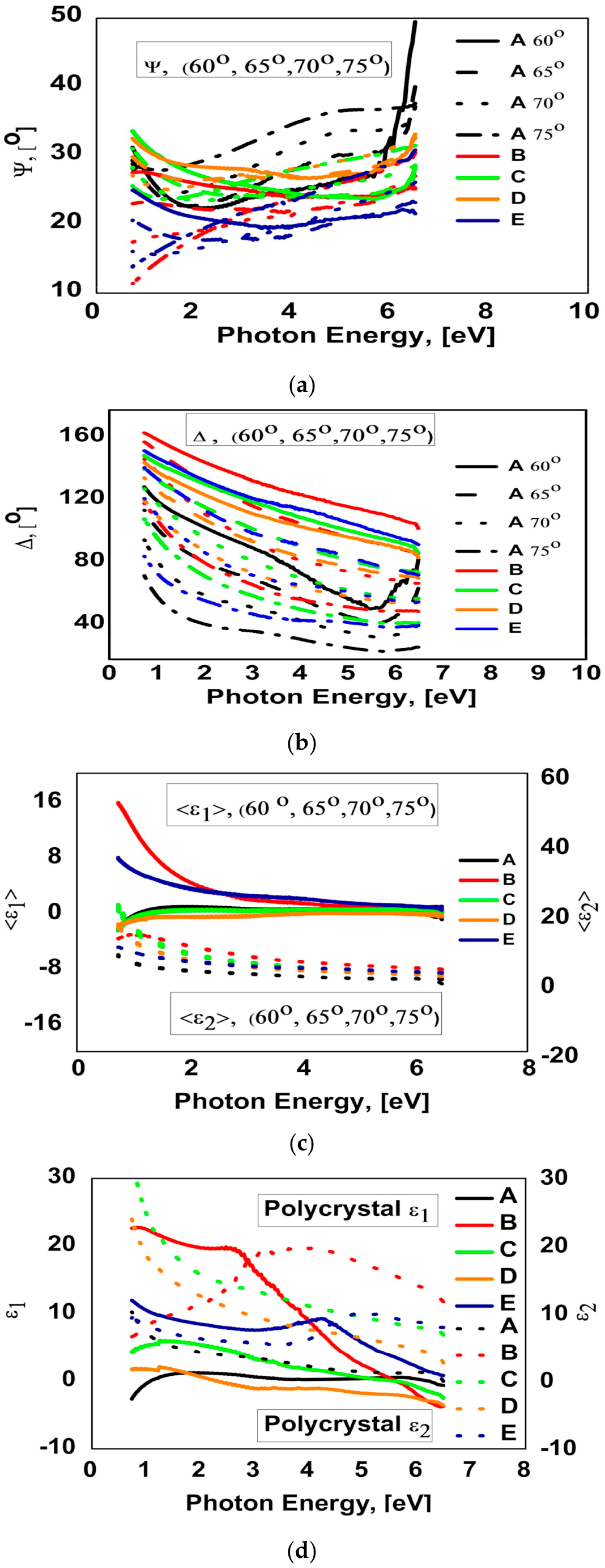
The results from the ellipsometry measurements and modelling are presented in
Figure 18. The technology experiments for deposition were carried out on the semi-industrial coating machine UDP850. Since the vacuum machine design did not allow the installation of in-situ ellipsometry equipment, it was only possible for ex-situ spectroscopic ellipsometry measurements to be performed. Technology experiments are expensive, and normally, such PVD vacuum machines are used in real industry-oriented projects. Our goal was that preliminary investigations of the optical properties of Cr-based complex hard coatings obtained in such projects on industrial-grade steel substrates are carried out. As the coatings are multicomponent, we intended to attempt to extract optical properties depending on the elements present in the coatings. SE measurements were taken at a single point of each sample with some variability in the ellipsometric angles, suggesting small variations in homogeneity. A serious limitation in our investigation was that our samples had rather high waviness and were macroscopically rough, as much as up to 10 µm RMS roughness over lateral areas of 2 cm × 2 cm. On the scale of an AFM measurement (lateral 10 µm × 10 µm), roughness was determined to be close to ~40 nm. The data are summarised in
Table 9.
The waviness of the samples was measured macroscopically with an optical Brucker Profilomer, and the data for Root Mean Square height
Sq and maximum height
Sz are shown in
Table 10. As can be seen, all the samples are characterised by high waviness. Measurements of the surface coating roughness taken on other samples deposited with similar industrial equipment and technology showed layers’ roughness around 20 nm [
49,
50,
51,
52]. As we performed one AFM measurement for sample D—Cr/CrN/CrTiAlN that had an almost similar value, we can assume that our industrial samples also have such roughness. As explained below, the huge macroscopic waviness value does not hamper the ellipsometric measurement and the roughness on the scale of the AFM measurement with adopted values around 20 nm can be well treated and handled with ellipsometric fitting for our industrial samples.
In
Figure 18, the measured values for Ψ and Δ are seen as a function of energy. Ellipsometry measures the ratio of the complex phase jumps of the reflected electromagnetic fields:
where
—Ratio of Fresnel reflection coefficients
—Fresnel reflection coefficient for p-polarized light
—Fresnel reflection coefficient for s-polarized light
—Electric field of incident light
—Electric field of reflected light
Ψ—amplitude ratio
Δ—phase difference
Since the Fresnel coefficients vary differently with the angle of incidence (AOI), Ψ and ∆ also depend on the angle of incidence (AOI). The substrate dielectric function can only be determined by direct inversion of the equations if there are no compound (e.g., with oxygen) overlayers present, if no preferential diffusion happens, and if roughness is eliminated. We assume that neither overlayers are present and that no preferential out-diffusion occurred, which is consistent with the XPS results (see
Figure 16).
In
Figure 18, the computed pseudodielectric function is also shown (<ε
1> and <ε
2>), which is obtained if the measured sample is assumed to be a perfect substrate. Since the single lines arising from the inversion of data taken at different angles of incidence are close but not perfectly overlapping, it is clear that an interfacial, i.e., roughness, layer has to be included. In addition, what can be immediately deduced from the pseudodielectric function is that no transparent overlayers (larger than 20 nm) are present because then interference effects would be seen.
Therefore, for extraction of the physical dielectric function, a microscopic roughness of approximately 20 nm was added in the modelling process, which acted as impedance damping for the electromagnetic fields (i.e., less reflection for the p- as well as s-polarised layers, also influencing their complex ratio). An advantage of our preliminary ellipsometric measurements and modelling results is as follows: Since our industrial samples are homogeneous with only ~20 nm roughness on an area of ~10 × 10 µm, which is approximately the same size as the spatial coherence area, the macroscopic waviness of a few µm does not need to be taken into account in the model for extraction of the real dielectric function, because EM fields reflected areas larger than 10 × 10 µm no longer interfere. This fact is also shown for industrial samples where quite small depolarisation of less than 20%, from 0.7 to 4.5 eV, is measured. Taking this into account, we trust our data in this wavelength range, but for completeness, modelling was performed for the full spectral range.
Modelling the surface roughness correctly in spectroscopic ellipsometry is the main factor for extracting acceptable optical constants. When the roughness of the samples is with dimensions of the spectroscopic ellipsometry wavelengths (>300 nm), the reflected optical signal from the rougher surface cannot be calculated properly and could lead to misleading values of the optical constants [
53]. As our coating samples have a surface roughness of 40 nm measured with AFM, a small influence on the dielectric function is expected, and a simple model of the roughness could be applied. Normally, in an effective medium approximation (EMA) model, a mixture of 50% material—having the dielectric function of the simulated layer—and 50% void space with the dielectric function of vacuum is applied [
54].
On the basis of these prerequisites, it was possible to set up an experimental model consisting of a bulk hard coating overlaid with a 20 nm wide “rough” layer. i.e., a mixture of 50% air and 50% hard coating modelling roughness. Then, we first fitted the data, always using a Drude model (three parameters) and an oscillator (four parameters). When the ellipsometric angles Ψ and Δ were well reproduced, we changed to well converging point-to-point fits for extracting the physical dielectric function. The results of these point-to-point fits are shown in
Figure 18. We are well aware that ellipsometric measurements have also been made before on similar hard coatings [
55,
56,
57,
58], and dielectric functions have been evaluated. As our samples are industrial ones, it follows that without prior polishing and etching for the minimisation of the steel substrate roughness, different deposition systems could produce a varying density, resulting in varying dielectric functions. We are aware that our measurements may differ from the references given. However, what has been surprising was that for non-polished samples, untreated as they are and directly taken from the stock, ellipsometry also proved to be a sensitive technique for distinguishing different process parameters. As mentioned before, our data are trustable (due to small depolarization factors) from 0.7 to ~4.5 eV, and we are now interpreting the results for AlN, CrN, and TiN in terms of interband transitions (arising from band structure effects and Van Hove singularities) as well as intraband transitions, best described by the Drude dispersion relation. Apart from roughness, investigations of the physical dielectric function of real industrial samples have to be conducted, keeping in mind that such layers are seriously influenced by factors such as homogeneity, density, thickness, etc. Each of these factors influences the optical properties of the layers and makes the analysis of interband transitions very complicated.
4. Discussion
Our research goal was first to obtain estimation results for our industrial Cr-based samples deposited with CFUBMS equipment. The possibility of extracting any dependencies and trends for more complex Cr-based coating configurations is motivation to proceed with more detailed research. At this stage, we have avoided numerous highly expensive real technology experiments for research on the optical properties of monolayers, binary, and triple coatings deposited with the CFUBMS equipment. Our conclusions are based on literature results from investigations of binary CrN, TiN, and AlN layers deposited using other techniques.
The optical properties of CrN have been previously investigated by other researchers. It has a direct bandgap of 1 eV. For this material, optical absorption is low for photon energies below 0.7 eV and increases steeply at higher energies [
59]. The same trend was observed in the real part of the dielectric function for the sample A—Cr/CrN in the range of 0.7–1 eV. It was also found that the dielectric function could give information about the existence of the Cr
2N and CrN phases because it is sensitive to the nitrogen content in the film.
On the other hand, Cr
2N films exhibit Drude metal-like behaviour with ε
1(ω) crossing the zero level at the plasma frequency. With the increase in N
2, the density of free electrons in the conduction band is reduced, and ε
1(ω) shows positive values [
60]. For sample A—Cr/CrN under 1 eV, ε
1(ω) is negative, and the crossing through 0 marks the Cr
2N and CrN phases. Almost the same trend, especially over 1 eV, applies to samples C—Cr/CrN/CrAlTiN-1 and D—Cr/CrN/CrTiAlN. The EDS results for these samples show that they have nitrogen composition under 50%, and a Cr
2N phase could be formed. The XPS results for the quaternary CrTiAlN coating (sample D—Cr/CrN/CrTiAlN) prove the existence of both Cr
2N and CrN phases.
For the coating of sample B—Cr/CrN/CAlN with composition Al 3.9 at. % measured with EDS, ε
1 has high values, suggesting the formation of an AlN phase whose band gap is 6 eV (207 nm) [
61]. The quaternary coating (sample E—Cr/CrN/CrAlTiN-2) with an Al content of 19.1 at. % by EDS also showed high ε
1(ω). The optical properties of the complex Cr-based layers with lower Al content are closer to those of CrN as it is in sample C—Cr/CrN/CrATilN-1 with 3.8 at. %. The trends of samples C—Cr/CrN/CrAlTiN-1 and D—Cr/CrN/CrTiAlN follow this trend but start from higher values because of the inclusion of Al in the coatings and formation of AlN phase as such was found in the XPS results for the quaternary sample D—Cr/CrN/CrTiAlN. When the current applied on the Cr target is increased, the ε
1 value is higher. The addition of Ti also influences the dielectric function of the compound structures. TiN has a direct bandgap of 3.4 eV [
62]. The dielectric function measured at room temperature is characterised by a sharp increase in ε
1(ω). It starts from a high negative value of −12.66 at 1.4 eV to a maximum value of 4.7 near 4.2V having typical free electron Drude behaviour [
63]. The Ti content in samples C—Cr/CrN/CrAlTiN-1, D—Cr/CrN/CrTiAlN, and E—Cr/CrN/CrAlTiN-2 could be the reason for the decreasing trends of the dielectric functions of these samples for energies higher than 1 eV. Formation of the TiN phase is seen for these coatings as it is in the XPS results for sample D—Cr/CrN/CrTiAlN. In all five sample curves, the real part of the dielectric function tends toward zero at higher energy levels. This is typical for the ε
1(ω) function of CrN-based coatings and is in agreement with the Drude model of metals. The ε
2(ω) trends of the dielectric function of the five samples also follow the decreasing trends seen in CrN layers [
64]. These authors have shown that the values of ε
2(ω) depend on the correlation between Cr and nitrogen. When the Cr and Cr
2N phases still exist, ε
2(ω) is higher. In our measurements of samples, C—Cr/CrN/CrAlTiN-1 and D—Cr/CrN/CrTiAlN with the lower composition of nitrogen ε
2(ω) start at the highest values. The starting levels of ε
2(ω) at the lower photon energies decrease with the increase in N
2 content in the layers and the formation of pure CrN, Sample A—Cr/CrN with the highest composition of nitrogen 66.5% (see
Table 3) has the lowest values of ε
2(ω). This result for ε
2(ω) suggests the existence of a mixture of different phases and compounds in the coatings.
In the spectral range from 1 to 2 eV, the values of ε2(ω) are distinguished from one another correspondingly to the composition of nitrogen in the coatings measured with EDS. The trends are decreasing except for samples B—Cr/CrN/CrAlN and E—Cr/CrN/CrAlTiN, which are deposited at higher Al current and have different Al content. The dielectric functions (ε1(ω) + iε2(ω)) were deduced from the measured data. Their variation clearly shows the dependence on the deposition conditions that lead to different compositions of the coatings composed mainly of Cr2N, CrN, TiN, and AlN proved in our XPS results.
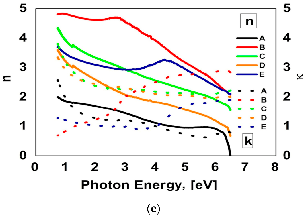
The complex refractive index n(ω) + iκ(ω) is formally equivalent to the dielectric function and is displayed here for convenience. It also depends on the nitrogen flow applied during the deposition process and formation of different phases, as shown for Cr
2N and CrN in [
64], and the trends for n(ω) and κ(ω) shown in
Figure 15. Comparing the data for CrN and Cr
2N, our data for these coefficients have lower values. As the authors of [
64] comment, the lower values of n(ω) for a layer are an indication of a less dense structure. Sample A with the lowest nanohardness showed the lowest n(ω), and the more complex structures showed higher n(ω) values, but their values do not show any direct correlation with the measured values for hardness and module of elasticity. Other authors do not attribute this spectral dependence to interband transitions [
65]. Literature data for n(ω) and κ(ω) for TiN layers show an increase in the photon energies of over 2.5 eV because of the response of the Drude electrons in the conduction band of TiN and below this range due to inter-band transitions. Such dependences for n(ω) were not observed in our Cr-based samples with the addition of Ti. The imaginary refractive index κ(ω) increases beyond 4 eV only for sample E. This coating has the highest content of Ti of 7.6 at. % measured with EDS.
The preliminary investigation of the optical properties of the Cr-based complex coating structures deposited under industrial conditions shows that they strongly depend on deposition conditions like target power and nitrogen flow. The materials (participating) in the structures forming different phases—Cr2N, CrN, AlN, and TiN—influence the curve trends. For the different Cr-based samples, specific trends were found. The trends are almost identical for the coatings with similar compositions. Distinguishing the trends to the precise concentration is not yet possible. It has to be performed for the different adhesion, transition, compound, and complex layers with less rough and very homogeneous samples. Such an experimental design will then allow interband transitions to be distinguished, which arise from either intermetallic compounds or the band structure of pure metals and intraband (Drude) contributions.
5. Conclusions
Five samples deposited with Closed Field Unbalanced Magnetron Sputtering for industrial applications were researched for their optical properties. The hardness of the samples was measured in the range of 15 to 23.8 GPa with a module of elasticity from 339 to 397 GPa. The coefficients of friction and the H/E and H3/E2 ratios were calculated, where sample D—Cr/CrN/CrTiAlN has shown the highest ratios of 0.059 and 0.085 [GPa]. The composition and morphology of the samples’ surfaces and grain sizes were characterised with SEM and EDS showing differences in the composition and the surface of the samples. The sample with the optimal combination of hardness of 21 GPa and resistance to scratch load up to 30 N without serious cracks or failure was chosen for additional investigation of composition with XPS and AES and structural morphology by TEM. The results show a homogeneous layer on the surface and in depth and the formation of the different sublayers of the coating. Cr2N, CrN, TiN, and AlN were the main compounds forming the coating layer. All five samples were characterised with UV-VIS ellipsometry, and their optical parameters Ψ and Δ were measured. An optical model was built, and the corresponding polycrystalline dielectric functions ε1(ω) and ε2(ω) and optical constants n(ω) and κ(ω) were calculated. The results show the dependences of the optical parameters on the variation of the deposition technological parameters and consequent composition of the samples, surface morphology, and participating compounds. The dielectric functions (ε1(ω) + iε2(ω)) of Cr-based coatings are dependent on the applied current to the Cr-target. The increase in the nitrogen flow increases the value of ε1(ω). The formation of phases of AlN and TiN influences the trends of dielectric functions. The complex refractive index n(ω) + iκ(ω) showed dependency on the nitrogen flow and the formed phases. The density is another important factor for the index. More detailed research on the Cr-based coatings and their composite layers is needed in order to predict the composition based on the measured optical properties and develop complex optical models. It is learned from the presented study that for industrial coatings with a surface roughness in the nm range and waviness in the µm range, surface analysis techniques probing the very surface can deliver the composition and chemical states of the topmost few nanometres; however, these parameters do not correlate directly with the usual quality criteria for hard coatings.
In conclusion, spectroscopic ellipsometry can be a useful technique for evaluating the composition and structural properties of Cr-based complex layers deposited at low temperatures under real industrial conditions; however, for more specific and detailed results, further investigations are necessary. Research with well-polished substrates has to be made so that hard coating layers have negligible roughness. Homogeneous industrial structures of thin layers, not beyond 200–300 nm, should be used, which are thick enough so that no interference effects occur. These (bulk) data can be used for the correlation of composition and structure to their dielectric function. If insulating and transparent precipitates occur (e.g., AlN nitrides), interference features will be enhanced. Because there is a variety of compounds and mixtures (Cr, Ti, and Al metal layers, binary CrN, TiN, and AlN nitrides, ternary compounds, such as CrAlN, TiAlN, CrTiN, as well as quaternary compounds), the establishment of optical database is strongly suggested and necessary. Corroborating measurements such as XRD, XPS, and TEM are needed in analysis in order to reveal structural transformations. And finally, for contactless conductivity measurements, the optical properties should also be investigated in the IR range. Following these points will then allow, by modelling and data fitting, the establishment of connections between the real deposition conditions, morphology, structure, and composition of the growing layers, mechanical properties and optical constants.
As we have obtained dielectric functions that are distinctively different for our five samples and we were able to distinguish them according to the inter-metallic CrN, AlN, and TiN compounds, we are convinced that, with more specific information, trustworthy results can be obtained about the optical properties of Cr-based coatings deposited under real industrial conditions with CLFUBMS equipment. These can be used in the future for inline control of the physical properties of the growing layers and real-time extraction of their composition if in situ ellipsometry equipment is installed in the PVD industrial equipment.
In this study, we aimed to study the optical properties of coatings deposited with closed field unbalanced magnetron sputtering intended for industrial applications. The obtained results are promising for the continued development of optical models for complex Cr-based hard coatings.
