Article

Study on the Forming Process and Properties of AlSi60 Alloy by Selective Laser Melting

1
School of Materials Science and Engineering, Southwest Jiaotong University, Chengdu 610031, China
2
Key Laboratory of Advanced Technologies of Materials, Ministry of Education, Chengdu 610031, China
3
Second Institute of China Aerospace Science and Technology Corporation, Beijing Institute of Radio Measurement, Beijing 100854, China
4
AVIC Chengdu Aircraft Industrial (Group) Co., Ltd., Chengdu 610073, China
5
Department of Aeronutics and Astronautics, Stanford University, Stanford, CA 94305, USA
*
Authors to whom correspondence should be addressed.
Coatings 2024, 14(3), 259; https://doi.org/10.3390/coatings14030259
Submission received: 9 February 2024 / Revised: 19 February 2024 / Accepted: 20 February 2024 / Published: 21 February 2024
(This article belongs to the Section Laser Coatings)

Abstract

:
Hypereutectic Al-Si alloys, which have a silicon content ranging from 12% to 70%, are a new generation of casing materials for chip packaging. They have broad applications in aerospace, weaponry, and civilian communications. Selective Laser Melting (SLM) offers significant advantages in achieving near-net shaping of complex casings. This paper presents a study on the formation defects, microstructure, and room temperature tensile properties of AlSi60 alloy prepared by SLM. The results indicate that the primary forming defects in the SLM AlSi60 alloy are balling, lack of fusion, and porosity. These defects are mainly influenced by the volumetric energy density. Samples of good quality can be produced within the range of 150 J/mm3 to 250 J/mm3. However, the same volumetric energy density can result in differences in sample quality due to various combinations of process parameters. Therefore, it has been determined that a well-formed AlSi60 alloy can be obtained within a laser power range of 300 W–350 W, scanning speed of 400 mm/s–800 mm/s, and hatch spacing of 0.09 mm–0.13 mm, with a density close to 98%. The microstructure of the SLM AlSi60 alloy consists of primary Si phases with irregular shapes and sharp edges measuring 5–10 μm, eutectic Si particles of 0.5 μm, and α-Al phases, with eutectic Si dispersed within the α-Al. The SLM AlSi60 alloy exhibits fine and evenly distributed primary Si phases with an average hardness of 203 HV. No significant anisotropy in hardness values was observed in the X and Y directions. The tensile strength of the alloy reached an average of 219 MPa, with an average elongation of 2.99%. During the tensile process, cracks initiated by the primary Si phases rapidly expanded, exhibiting minor ductile fracture characteristics in the Al phases. Due to the high volume fraction of Si phases, the tensile test was dominated by brittle fracture. The tensile curve only exhibited the elastic stage.

1. Introduction

The development of electronic technology has led to the evolution of microwave circuits and electronic components towards higher power, miniaturization, and increased complexity [1]. The integration improvement has resulted in a sharp rise in chip heat generation, causing the lifespan of GaAs or Si semiconductor devices to decrease by threefold for every 10 °C increase in temperature [2]. This thermal control issue imposes higher requirements on electronic packaging materials. The requirements for modern electronic packaging materials are threefold: a thermal expansion coefficient (CTE) in the range of 7–9 × 10⁻⁶ °C−1 to match GaAs or Si semiconductor devices, a thermal conductivity (TC) greater than 100 W/(m·K) to prevent device failure due to excessive temperatures, and a density maintained below 3 g/cm3 to meet lightweight requirements [2,3]. Hypereutectic Al-Si alloys can adjust the Si content, which allows them to have both the high thermal conductivity of Al and the low thermal expansion coefficient of Si. As a result, this material meets the requirements for low thermal expansion, high thermal conductivity, and low density, making it a promising new type of electronic packaging material.
The preparation methods for hypereutectic Al-Si alloys include melting casting, infiltration, powder metallurgy, and spray forming [3]. Melt casting is suitable for mass production, but results in coarse primary Si phases due to slow cooling rates, which reduces the plasticity and toughness of the alloy [4]. The addition of modifiers such as Ce [5], Sr [6], and P [7] can refine the Si phase and effectively enhance mechanical properties. However, when the silicon content exceeds 25 wt.%, adding modifiers is insufficient to refine the primary silicon phase [8]. Infiltration includes pressure and non-pressure methods [9]. Although they can achieve near-net shaping, the limitations of liquid flow prevent the formation of parts with specific shapes, requiring secondary processing. Powder metallurgy can refine silicon particles and achieve a uniform distribution, but it is prone to oxidation of active aluminum powder during the process. Under an inert atmosphere, the formation of a stable oxide film cannot be reduced or broken, which can negatively affect performance [10]. Spray forming can reduce the diffusion and segregation of solute atoms, achieving a non-segregated, fine-grained structure [11]. However, samples produced by spray forming require subsequent hot isostatic pressing to eliminate internal porosity, which increases production costs.
Selective Laser Melting (SLM), as an innovative additive manufacturing (AM) technology, eliminates the need for molds in the forming process and showcases immense potential in directly fabricating complex three-dimensional parts, and the residual metal powder utilized during the forming can be recycled, thereby enhancing the efficiency of material usage [12,13,14]. This effectively overcomes the disadvantages associated with traditional high silicon–aluminum alloy preparation methods, such as melting casting, infiltration, powder metallurgy, and spray forming, which are characterized by long cycles and high costs. Besides, SLM provides cooling rates of up to 104–105 K/s, while the cooling rate of conventional melting processes such as casting is typically less than 100 K/s [15]. Therefore, SLM can generate finer grains and substructures within the grain, which improves the overall mechanical performance of the final components [16]. Research extensively covers SLM-formed titanium alloys [17,18], high-temperature nickel-based alloys [19,20], and iron-based alloys [21]. For aluminum alloys, research has focused on Al-Si alloys, with extensive studies already conducted on the processes, microstructures, properties, and post-treatments of AlSi10Mg [22,23,24] and Al-12Si [25,26]. Research conducted by Zhang et al. [22] reveals that the tensile strength of the AlSi10Mg alloy, synthesized through SLM, can ascend to 500 MPa, significantly surpassing the benchmarks set by traditional casting methods. Moreover, the tensile strength and elongation rate of the alloy can be finely tuned via heat treatment. In a parallel vein, Prashanth et al. [25] have illustrated that strategic annealing treatment is capable of modulating the mechanical properties of Al-12Si, enabling enhancements in both strength and ductility across a broad spectrum. Upon enhancing the silicon content, the disparities in physical properties between silicon and aluminum become markedly pronounced, thereby significantly influencing the alloy’s forming behavior. At present, scholarly inquiry into hypereutectic Al-Si alloys, particularly those with silicon content surpassing 50%, is markedly scant. Furthermore, extant studies have predominantly concentrated on investigating processes, microstructural characteristics, and thermal-physical properties [27,28,29]. Jia et al. [27] demonstrated in their study on AlSi50 that SLM can refine the primary Si phase to approximately 5 μm, a significant reduction from the 220 μm observed in traditional casting methods. Nang Kang et al. [28], in their study of the SLM-formed AlSi50 alloy, also confirmed the primary Si phase size to be 5 μm. Their examination of hardness and wear properties revealed that at a laser power of 320 W, the sample’s maximum hardness reached 188 HV, and at 350 W, it exhibited the lowest wear rate of 5.5 × 10⁻⁴ mm3 N−1 m−1. Hanemann et al. [29] compared the CTE of AlSi25 and AlSi50, demonstrating that Si content can effectively modify the CTE, resulting in a reduction of 0.2 × 10⁻⁶ 1/K for each wt% increase in Si. In the realm of hypereutectic aluminum–silicon alloys, particularly those with silicon content surpassing 50%, investigations into mechanical properties, notably tensile properties and fracture mechanisms, remain exceedingly sparse.
Consequently, to meet the complex fabrication demands of semiconductor devices utilizing an AlSi60 alloy, this research meticulously investigates the impact of laser processing parameters on the quality of formations produced through the SLM of an AlSi60 alloy. The analysis encompasses the microstructural composition and characteristics of SLM-prepared AlSi60, examines the hardness distribution and tensile properties of the SLM-formed AlSi60 alloy, and further elucidates the tensile fracture mechanism of AlSi60. This furnishes both technical and theoretical underpinnings for the SLM forming process of the AlSi60 alloy, contributing to the broader understanding and application of this material in semiconductor device fabrication.

2. Experimental Details

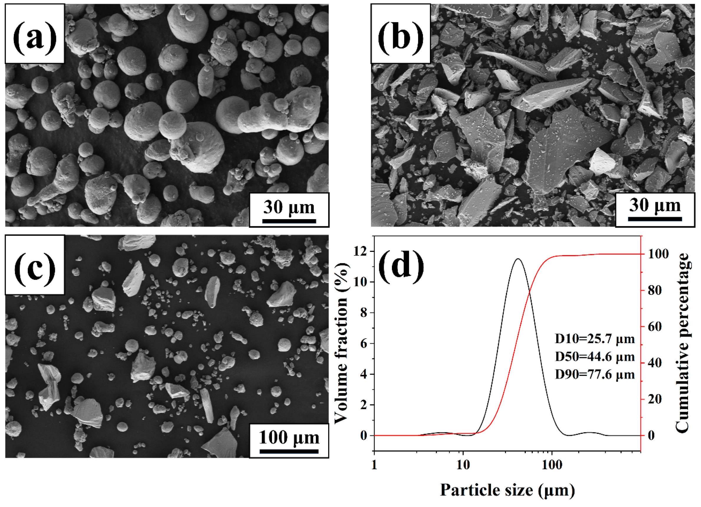
2.1. Powder Preparation

The experimental AlSi60 alloy powder was synthesized by blending 40% pure Al powder with 60% pure Si powder, each possessing a purity of 99.99%. As illustrated in Figure 1, the morphology and particle size distribution of the powder indicate that the Al powder, synthesized via gas atomization, predominantly exhibits a spherical form accompanied by some satellite particles; conversely, Si powder, attributed to its brittle nature, is manufactured into irregular shapes through a crushing process. The Al and Si powders were mechanically blended in the stipulated ratio to yield the powder composition showcased in Figure 1c. The particle size distribution of the AlSi60 powder was quantified utilizing a laser particle size analyzer (Malvern Mastersizer 3000, Malvern Panalytical, Malvern, UK), revealing measurements of D10 = 25.7 μm, D50 = 44.6 μm, and D90 = 77.6 μm. These specifications are suitable for SLM experiments. To augment the powder’s flowability and mitigate the influence of moisture on the SLM forming quality, the powder underwent drying in a vacuum oven at 80 °C for a duration of 2 h prior to experimentation.

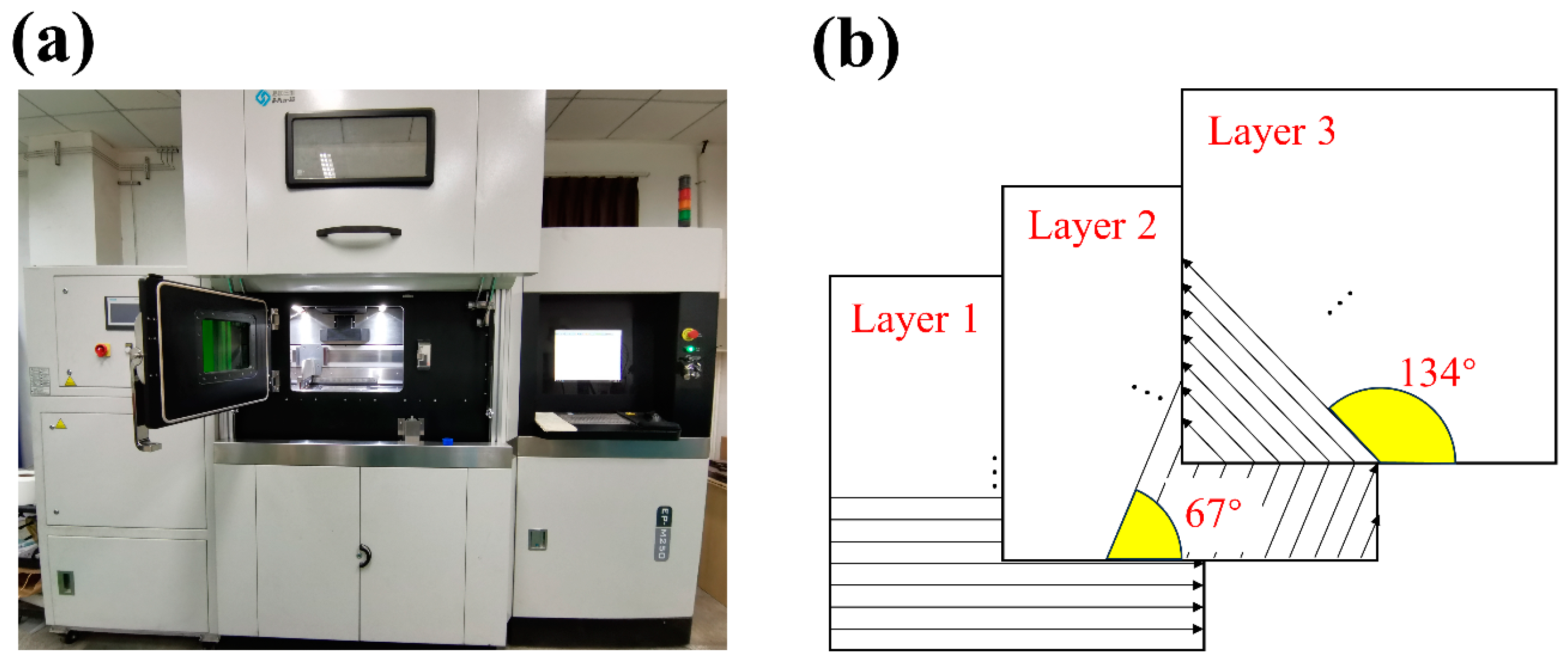
2.2. SLM Fabrication

SLM experiments were conducted on a commercial EP-M250 device (Beijing Eplus3D Technology Co., Ltd., Beijing, China), as shown in Figure 2a, with a maximum build size of 258 mm × 258 mm × 350 mm, laser wavelength of 1070 nm, focus spot diameter of approximately 70 μm, maximum power up to 500 W, scanning speed up to 7 m/s, and layer thickness ranging from 0.02 mm to 0.1 mm. In the SLM experiments, the powder layer thickness was fixed at 30 μm, and each layer was filled using a long straight line scanning strategy, as illustrated in Figure 2b, with the scanning direction of adjacent layers rotated by 67°. Argon gas was continuously supplied during the printing process to ensure the oxygen content in the chamber remained below 1000 ppm, thereby reducing the impact of oxygen on the forming quality. The study investigated the effects of three main process parameters on the forming quality of AlSi60: laser power, scanning speed, and hatch spacing. The laser power ranged from 150 W–450 W, with increments of 50 W, selecting seven parameters in total; scanning speed ranged from 400 mm/s–1200 mm/s, with increments of 200 mm/s, selecting five parameters in total; hatch spacing ranged from 0.03 mm–0.13 mm, with increments of 0.02 mm, selecting six parameters in total. To facilitate the study of the impact of process parameters on forming quality, a full factorial experiment was employed, creating 210 combinations of process parameters. The optimal process parameters were determined through the analysis of surface quality, internal quality, and density of 5 mm × 5 mm × 5 mm cubes.

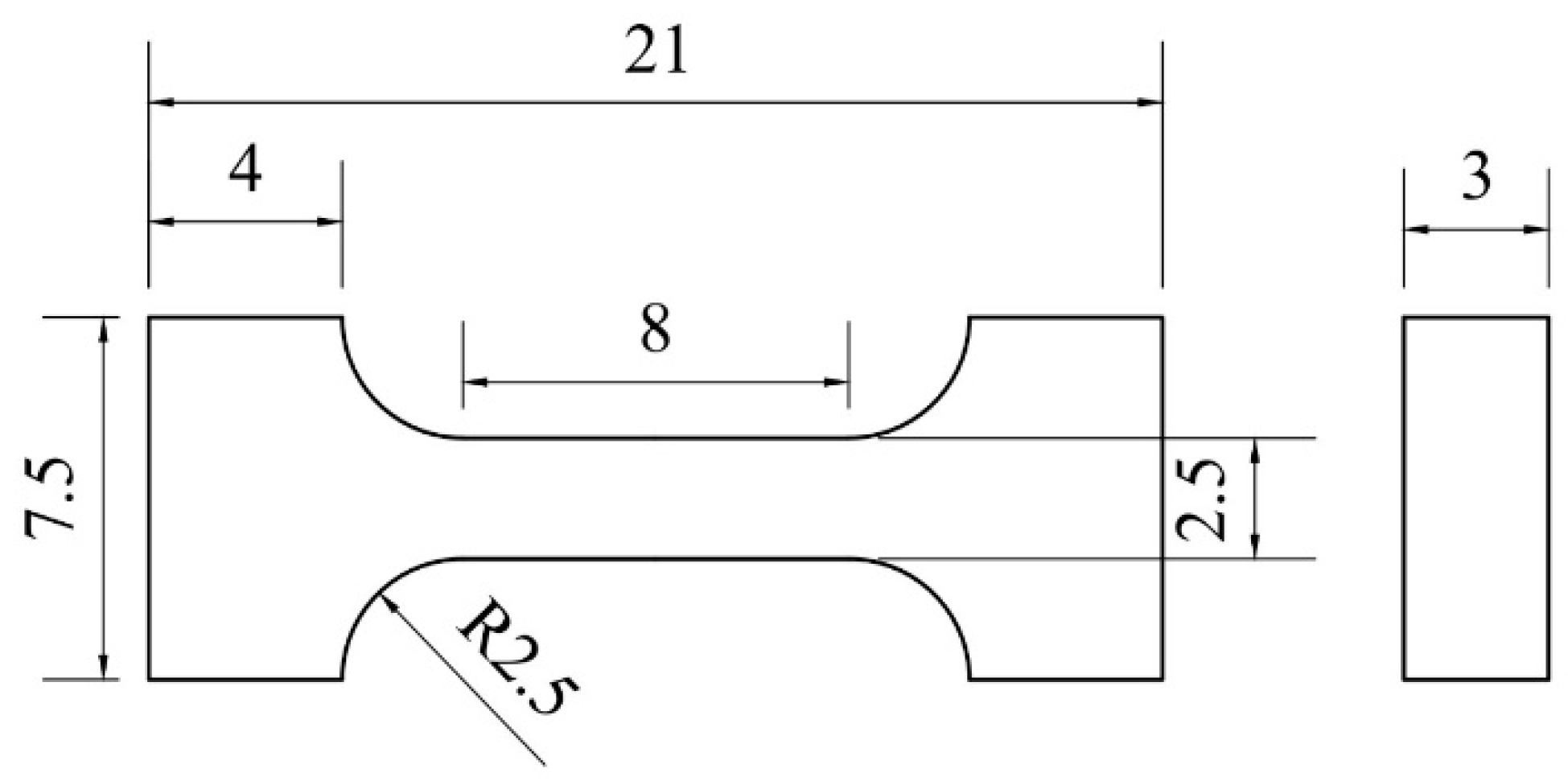
2.3. Characterization and Testing

For the obtained SLM samples, a stereo microscope (Stemi 2000-C, Zeiss, Oberkochen, Germany) was used to observe the surface morphology. The samples were sequentially pre-polished with 240#, 400#, 600#, 800#, 1200#, 1500#, and 2000# grit sandpapers, followed by surface polishing using a diamond spray polisher with a granularity of W1.0. Subsequently, internal defects of the samples were observed using an optical microscope (ZEISS AxioObserver A1m, Zeiss, Oberkochen, Germany). The actual density of the samples was measured using the Archimedes principle. Before measuring the actual density, each surface of the sample was polished to obtain a smooth surface, and ultrasonic cleaning was used to prevent stains and residual particles. Using an electronic densitometer (DX-100E, Qingdao Toky Instruments Co., Ltd., Qingdao, China), the mass of the dried sample in air and the mass of the sample fully immersed in distilled water were measured, ultimately determining its actual density value. Each sample was measured three times, and the average value was taken as the final density. The relative density was obtained by dividing the measured density by the theoretical density, which is taken as 2.47 g/cm3. The obtained metallographic samples were etched using Keller’s reagent with a composition of H2O:HCl:HNO3:HF = 95:1.5:2.5:1 for 20 s. The scanning electron microscope (SEM, ZEISS Gemini 300, Zeiss, Oberkochen, Germany) A ZEISS Gemini 300 was used to observe the microstructure, and elemental analysis of the samples was performed using the energy dispersive spectrometer (EDS, SmartEDX, Zeiss, Oberkochen, Germany). An X-ray diffractometer (XRD, SmartLab, Rigaku Corporation, Akishima-shi, Jaban) was used to analyze the phase composition of SLM-formed AlSi60, with a scanning range of 20°–100° and a scanning rate of 2°/min. Phase calibration was performed using a transmission electron microscope (TEM, FEI Talos F2000X, FEI Company, Hillsboro, OR, USA). Microhardness testing of SLM-formed AlSi60 was conducted using a Vickers hardness tester (HVS-30, Jinan Kason Testing Equipment Co., Ltd., Jinan, China) with a load of 1 kg and a dwell time of 15 s. The spacing between adjacent hardness points was 0.2 mm, within a test range of 4 mm × 4 mm. A hardness contour map was generated using Origin software based on the obtained hardness points. Tensile samples were obtained perpendicular to the deposition direction. Specimens with a width of 7.5 mm and thickness of 3 mm were designed according to GB/T 228-2002 and specific dimensions as shown in Figure 3. A microcomputer-controlled electronic universal testing machine (CMT5105, Shenzhen Sans Material Test Instrument Co., Ltd., Shenzhen, China) was used to test the tensile strength of the formed samples at room temperature.

3. Results and Discussion

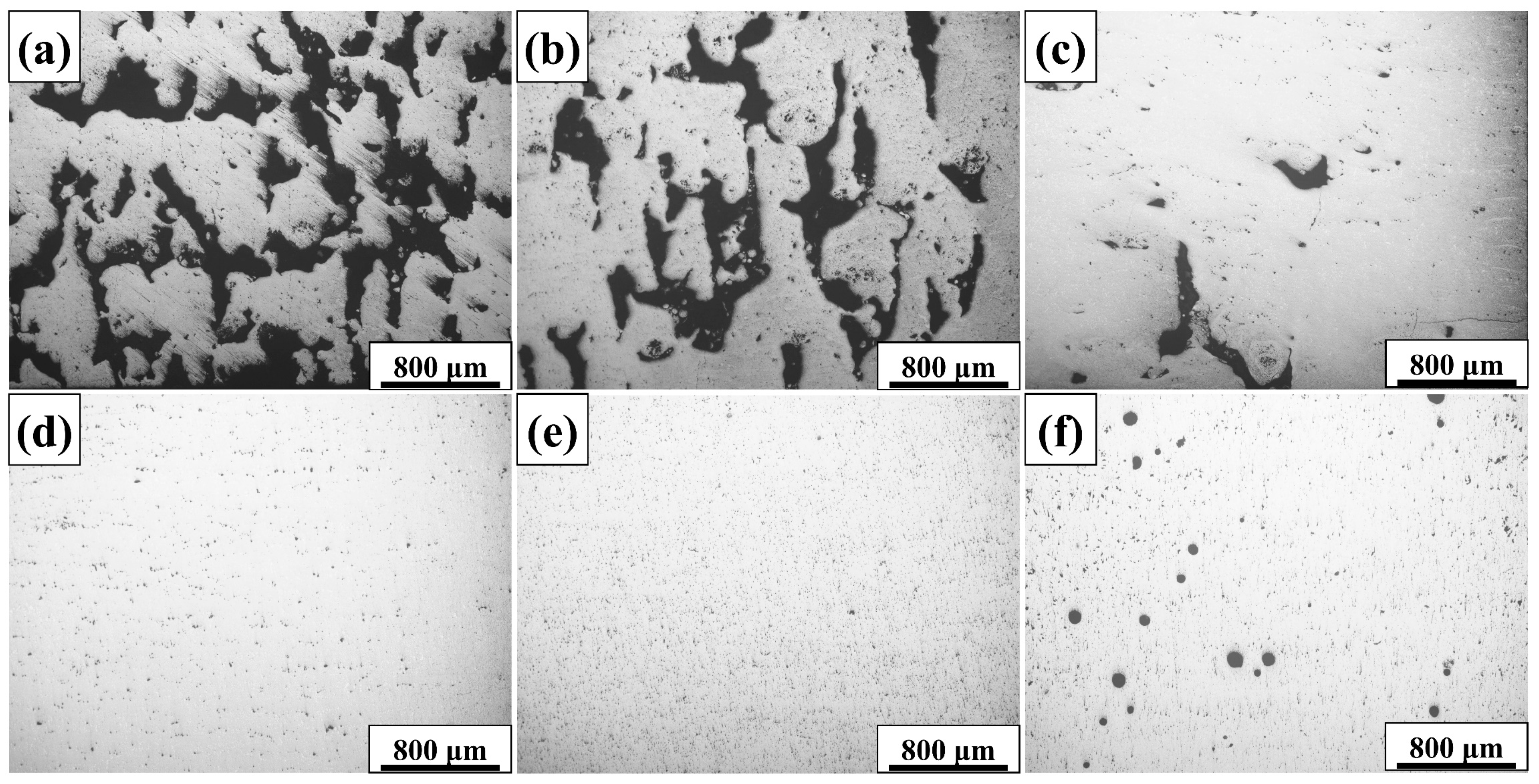
3.1. Effect of Process Parameters on SLM Forming of AlSi60 Alloy

Volumetric energy density is a comprehensive indicator related to laser power, scanning speed, hatch spacing, and powder layer thickness, defined by the formula:
E = P v h t
where  P  is the laser power (W),  v  is the scanning speed (mm/s),  h  is the hatch spacing (mm), and  t  is the print layer thickness (mm).
Throughout the forming process, the impacts of laser power, scanning speed, and hatch spacing on forming quality exhibit a complex interrelation. Consequently, volumetric energy density is frequently employed as a normalization factor in analyses aimed at elucidating the effects of process parameters on forming quality. Representative surface morphologies under different volumetric energy densities are shown in Figure 4. The main defects in the surface morphology are balling defects. The first type, comprising larger balling defects that span from 200 μm to 600 μm, manifest in Figure 4a–c, is attributable to diminished melt wettability at reduced laser energy densities, which hinders its complete dispersion across the substrate or atop the preceding layer. As the volumetric energy density escalates, there is a gradual diminution in the prevalence of the first type of balling defects. Upon reaching a volumetric energy density of 177 J/mm3, as depicted in Figure 4d, the initial variant of balling defects vanishes, yielding an optimally formed surface morphology. As the volumetric energy density is augmented to 222 J/mm3, evident in Figure 4e, smaller balling defects, measuring less than 100 μm, emerge on the sample’s surface. The emergence of the second variety of balling defects is predominantly attributed to the excessive volumetric energy density inducing instability within the melt pool. Upon further increasing the volumetric energy density to 265 J/mm3 in Figure 4f, the sample surface begins to exhibit unevenness distinct from balling, due to the significant thermal stress generated by overheating of the sample.
Surface defects in the formed samples can significantly degrade the powder spreading quality in the SLM process, leading to the formation of internal defects. The internal defects primarily encompass lack of fusion defects and porosities. Lack of fusion defects, as depicted in Figure 5a–c, diminish in prevalence with an increment in volumetric energy density. The internal lack of fusion defects disappear when the volumetric energy density increases to 177 J/mm3. The presence of surface balling defects reduces the quality of SLM powder spreading, resulting in many areas lacking fusion. Insufficient laser energy density causes poor wettability of the melt, leading to failure to spread and fill the unfused areas, resulting in numerous lack of fusion defects. Although surface balling defects also exist in Figure 4e, the impact of small-sized balling is limited. With elevated volumetric energy densities, the enhanced wettability of the melt facilitates the complete infilling of unfused areas, thereby obliterating the lack of fusion defects in the internal morphology depicted in Figure 5e. However, compared to the internal morphology of Figure 5d, Figure 5e has more small-sized pores internally. The internal morphology in Figure 5f contains numerous irregular pores and spherical porosity defects ranging from 50 μm to 100 μm. Irregular pore defects stem from surface expansion deformation, whereas spherical porosity defects arise due to the overheating and subsequent vaporization of the metal powder within the melt pool during the SLM process. Under conditions of elevated temperature and pressure, gas and plasma within the pore undergo violent expansion, leading to an eruption. The subsequent reduction in gas content precludes the maintenance of the pore structure, initiating a gradual closure that encapsulates metal vapor and protective gas, culminating in the formation of a porosity defect.
The manifestation of surface balling defects significantly influences the incidence of internal lack of fusion defects and porosities, consequently diminishing the density of the fabricated samples. Hence, density is used to characterize the forming quality of the samples. Figure 6 delineates the influence of volumetric energy density on the density of the samples. Within a volumetric energy density range of 150 J/mm3 to 250 J/mm3, numerous parameters facilitate the achievement of densities exceeding 97%, aligning with the internal morphology observations devoid of lack of fusion defects depicted in Figure 5d,e. However, volumetric energy density constitutes a simplification of the intricate relationship among parameters including laser power, scanning speed, and hatch spacing. Identical volumetric energy densities can be attained through diverse combinations of process parameters, resulting in variations in the forming quality of samples. Additionally, Figure 6 illustrates that a consistent relationship between volumetric energy density and sample density is not maintained, suggesting that the identification of an optimal process window cannot rely solely on the preferred range of volumetric energy density.
In pursuit of delineating the optimal process window for forming, a study was conducted on the relationship between laser power, scanning speed, hatch spacing, and density, with the findings illustrated in Figure 7. Figure 7a–f consistently demonstrates the influence of laser power on density, highlighting a rapid augmentation in density as laser power escalates from 150 W to 300 W, a subsequent stabilization between 300 W to 350 W, and a minor reduction upon surpassing 350 W of laser power. This phenomenon can be attributed to the fact that an elevation in laser power contributes to an augmented volumetric energy density. Combined with the relationship between lack of fusion defects, porosities, and volumetric energy density shown in Figure 5, the gradual disappearance of lack of fusion defects results in a rapid increase in density. Upon the internal elimination of lack of fusion defects, density achieves stabilization; however, the ensuing emergence of spherical porosities precipitates a decline in density. Therefore, the optimal range of laser power is between 300 W–350 W.
The effect of scanning speed on density is more noticeable when laser power is at a lower level of 150 W–250 W. The general trend suggests that decreasing scanning speed can increase density. At lower laser power levels, the depth of the laser-melted powder is insufficient. This causes the loose powder at the bottom of the melt pool to lack restraint, resulting in a higher tendency for surface balling and a larger number of unfused areas internally. Reducing the scanning speed increases the amount of time the laser is exposed to the powder, which increases the wettability of the melt and effectively fills in the unmelted areas, resulting in a significant increase in density. At higher laser power levels, where internal lack of fusion defects are absent, scanning speed predominantly influences the stability of the melt pool. An excessively rapid scanning speed undermines the stability of the melt pool, escalates the likelihood of spattering, and consequently diminishes the density. Therefore, a relatively slower scanning speed of 400 mm/s to 800 mm/s needs to be selected.
Hatch spacing is defined as the distance between adjacent melt tracks, influencing the overlap rate among these tracks, whereas the width of the melt tracks is ascertained by the interplay of laser power, scanning speed, and laser spot diameter. In Figure 7, the impact of hatch spacing on density is minimal, with significantly lower density values occurring only under conditions of 150 W laser power and 1200 mm/s scanning speed, as shown in Figure 7e,f. This phenomenon occurs because excessive hatch spacing leads to insufficient overlap between melt tracks, causing discontinuities in the surface morphology, inadequate melting of powder between melt tracks, and an excessive number of internal lack of fusion defects. Conversely, when hatch spacing is too small, accumulation between melt tracks occurs easily, and at high laser power and low scanning speed, excessive volumetric energy density can lead to the expansion deformation seen in Figure 4f. Therefore, considering the optimal ranges of laser power and scanning speed, the optimal hatch spacing range is determined to be 0.09 mm to 0.13 mm.
Therefore, as shown in Table 1, the optimal processing window for the SLM forming of the AlSi60 alloy is defined as: laser power of 300 W–350 W, scanning speed of 400 mm/s–800 mm/s, hatch spacing of 0.09 mm–0.13 mm, and volumetric energy density range of 150 J/mm3 to 250 J/mm3.

3.2. Microstructure and Properties

3.2.1. Phase Analysis and Microstructural Characterization

Based on the optimal process parameter range obtained in Section 3.1, AlSi60 samples were prepared using a laser power of 350 W, scanning speed of 600 mm/s, hatch spacing of 0.11 mm, and volumetric energy density of 177 J/mm3. XRD was used to analyze the phases of the AlSi60 alloy, with results shown in Figure 8. The blue Si peaks in the standard PDF#27-1402 card match the 2θ values of 28°, 47°, 56°, 69°, 76°, 88°, and 95° and the red Al peaks in PDF#01-1108 at 2θ values of 39°, 45°, 65°, 78°, 82°, and 99°. Based on the material composition, it can be deduced that the sample mainly consists of Al and Si phases. In addition, no apparent alloying phases of aluminum and silicon were found in the XRD spectrum, possibly because there was no metallurgical reaction between them, or if there was, the amount was too small to be detected by XRD. Furthermore, according to Figure 8, the main diffraction peak intensity of the Si phase is significantly higher than that of the Al phase. This discrepancy may be attributed to a higher proportion of the Si phase within the alloy composition and the vaporization tendency of Al during the melting process, culminating in an elevated percentage of Si content.
Further analysis of the phase composition of the AlSi60 alloy reveals that, according to the Al-Si binary phase diagram [30], the SLM forming process of the AlSi60 alloy first precipitates the primary Si phase. Subsequently, a eutectic reaction occurs at the eutectic temperature of 577 °C, resulting in the precipitation of the eutectic (α-Al + Si). Ultimately, the microstructure consists of the primary Si phase and the eutectic (α-Al + Si). The formation process can be represented as L → L + Sip → (Sie + α-Al) + Sip, where Sip represents the primary Si, and Sie denotes the eutectic Si [31].
The microstructural morphology of the AlSi60 alloy was analyzed. The metallographic organization and SEM images at low magnification, shown in Figure 9a,b, indicate a uniform distribution of the primary Si phase throughout the alloy. The size of the primary Si phase is limited to between 5–10 μm due to the rapid melting and solidification during the SLM process, which inhibits grain growth. Compared to the 30 μm grain size typically obtained with spray forming processes [32], the fine and uniform microstructure achieved through SLM contributes to improved mechanical properties such as strength and hardness. This uniformity is beneficial for aerospace components that undergo significant stress and for communication devices where consistent performance is essential. The growth mode of the primary Si phase in hypereutectic Al-Si alloys involves dislocations promoting continuous spiral growth (DPCS) and twin plane re-entrant edge (TPRE) growth mechanisms [33], resulting in primary Si phases being polyhedral crystals in three-dimensional space, primarily octahedral with {111} crystallographic planes. Consequently, high-magnification SEM images (c) reveal primary Si phases of varying sizes and morphologies, characterized by sharp edges. Due to the presence of α-Al and eutectic Si in the eutectic (α-Al + Si), which are difficult to distinguish in high-magnification SEM images, EDS spectral analysis shown in Figure 9d indicates that the eutectic Si phase is granularly distributed on the α-Al matrix. The distribution is uneven, mainly concentrated near the primary Si phases.
Subsequent TEM examination of the AlSi60 alloy found numerous grooves forming inclined steps, as indicated by the arrows in Figure 10a, and grooves were also found on the primary Si phase in Figure 10b,e. Research indicates that stable grooves on twin planes facilitate the rapid growth of the primary Si phase in a specific direction [34]. The high-resolution image of the area marked by the red circle in Figure 10b, shown in Figure 10c, clearly reveals these steps, indicating the growth steps of the primary Si phase and proving the TPRE growth mode of the primary Si phase. Figure 10d shows the diffraction pattern of α-Al, with the crystallographic axis direction being [ 1 ¯ 1 ¯ 0 ]. In Figure 10e, grooves indicated by arrows were also found, and the entire Si phase is of a larger size, indicating it to be the primary Si phase. The diffraction pattern calibration results show the crystallographic axis direction as [ 0 1 ¯ 1 ]. Figure 10f shows the distribution of eutectic Si particles on the α-Al phase, with the eutectic Si particles being less than 0.5 μm in size, belonging to the nanometer-sized Si phase. The diffraction pattern results indicate the crystallographic axis direction as [211].

3.2.2. Microhardness

Figure 11 shows the microhardness contour map of the SLM-formed AlSi60 alloy. The hardness values in the X and Y directions do not exhibit significant anisotropy, with an average microhardness value of 203 HV. This is a significant improvement compared to the microhardness of 150 HV for the AlSi60 alloy prepared by spray forming [32]. Research conducted by Zhao et al. [35] suggests that a diminutive size of the primary Si phase correlates with elevated microhardness levels. The average diameter of the primary Si phase in the AlSi60 alloy, when prepared through spray forming, can be diminished from 30 μm to approximately 10 μm following hot extrusion. However, it is challenging to ensure a uniform distribution of the primary Si phase on the eutectic matrix after extrusion, resulting in a lower microhardness compared to the AlSi60 alloy formed by SLM.

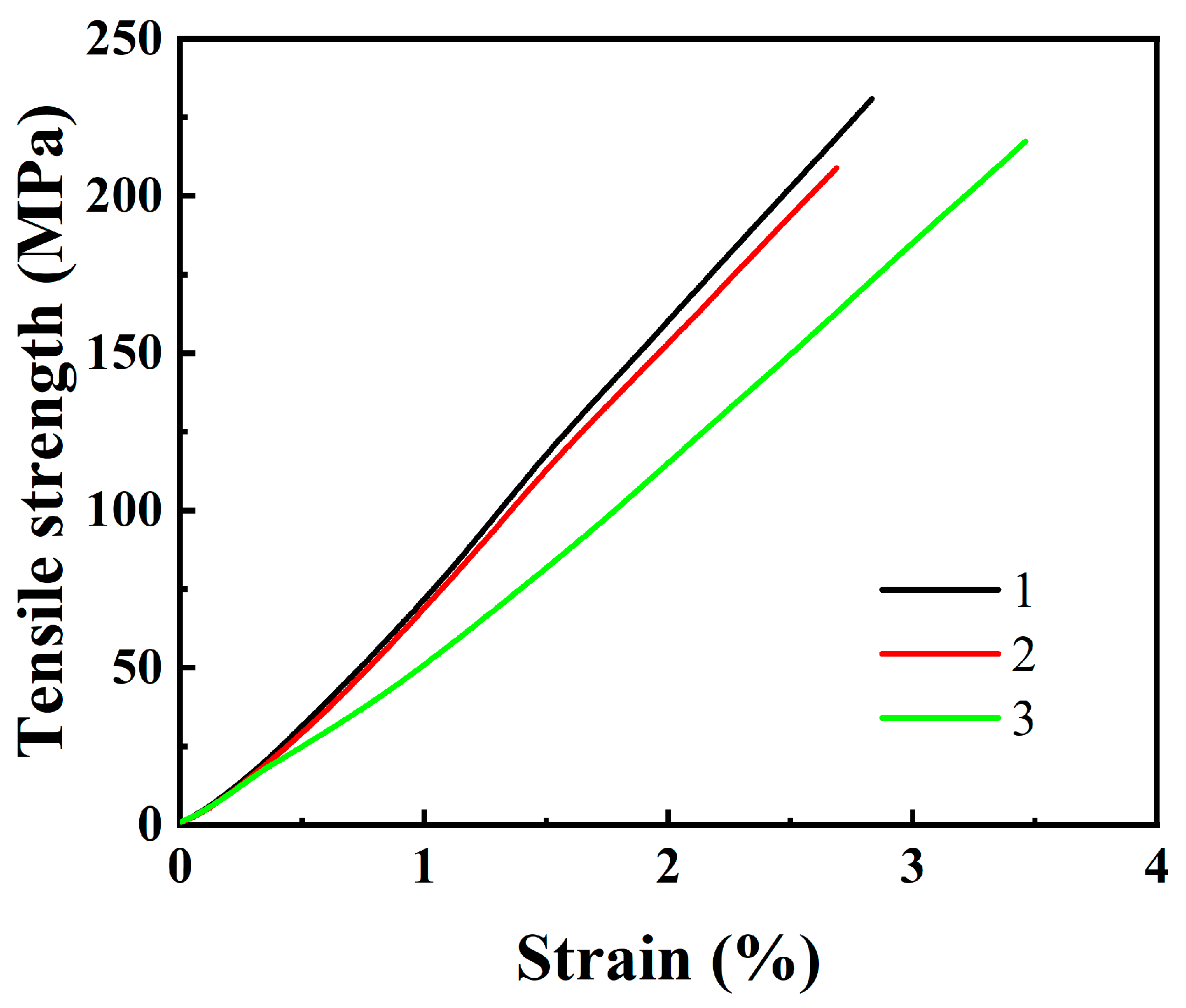
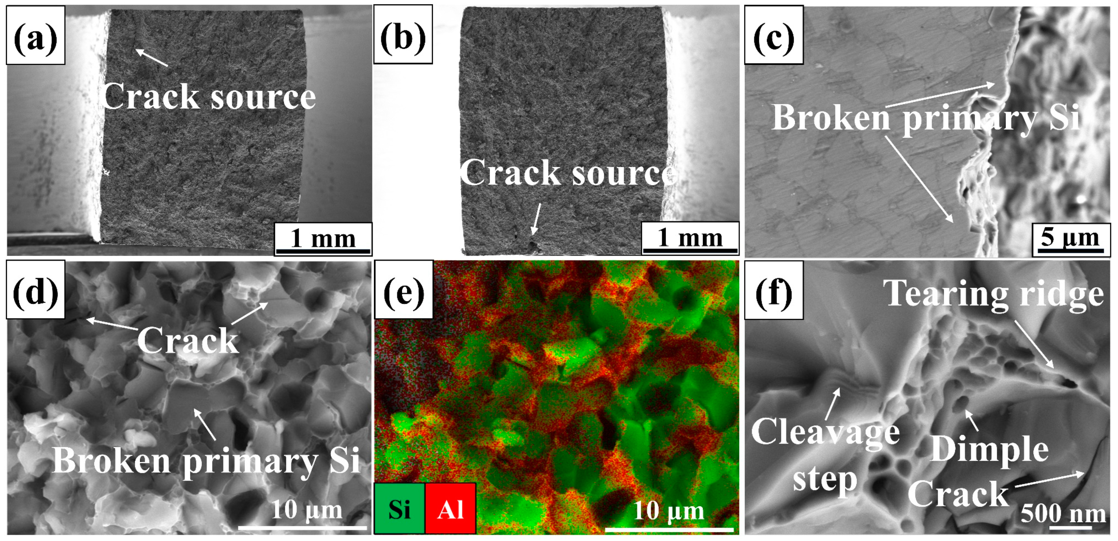
3.2.3. Tensile Properties and Fracture Mechanism

Three tensile tests were conducted on the SLM-formed AlSi60 alloy, with the results shown in the stress–strain curve of Figure 12. As shown in Table 2, Sample 1 had a tensile strength of 231 MPa and an elongation of 2.83%, Sample 2 had a tensile strength of 209 MPa and an elongation of 2.69%, and Sample 3 had a tensile strength of 217 MPa and an elongation of 3.46%. The average tensile strength of the samples was 219 MPa, with an average elongation of 2.99%.
The tensile strength after spray deposition was only 91 MPa, and although it could be increased to 164 MPa [32] after extrusion treatment at 520 °C, it was still lower than the 219 MPa tensile strength of the AlSi60 alloy formed by SLM. The primary Si phase grains formed by SLM were fine, with sizes below 10 μm. In contrast, the average size of the primary Si phase formed by spray forming was 30 μm, and the average size remained above 10 μm even after hot extrusion treatment [32]. Therefore, according to Equation (2) [36] relating alloy strength to the number and size of grains, the fine size of the primary Si phase obtained by SLM is the reason for the increased tensile strength.
σ φ V d 1 ( 1 φ V ) 1
where  σ  is the strength of the alloy,  φ V  is the volume fraction of the reinforcing phase, and  d  is the average diameter.
On the other hand, the rapid melting and solidification characteristic of SLM results in a high-temperature gradient, while the thermal expansion coefficients of Al and Si are 23.6 × 10⁶/K and 4.1 × 10⁶/K, respectively [3]. The mismatch in thermal expansion behavior can lead to residual stresses and the formation of numerous dislocations due to deformation differences during temperature changes. A large number of dislocations exist at the interface between the α-Al matrix and the primary Si phase, resulting in dislocation strengthening and thereby increasing the alloy’s tensile strength.
The entire stress–strain curves obtained from the three tensile tests exhibited only the elastic stage, which is due to the increase in Si content significantly enhancing the alloy’s hardness and strength but also reducing the material’s ductility, leading to increased brittleness. Furthermore, the sharp edges characteristic of the primary Si phase morphology also make the AlSi60 alloy more prone to fracture during tensile testing, resulting in the stress–strain curve exhibiting only the elastic stage.
Analysis of the tensile fracture reveals that the SLM-formed AlSi60 alloy exhibits clear characteristics of brittle fracture due to the high Si content, with a smooth fracture surface perpendicular to the direction of tension, and no significant plastic deformation in the macroscopic morphology. Figure 13a shows that the crack originated on the sample surface and gradually expanded inward. Figure 13b indicates that the crack propagated through a surface notch. Figure 13c shows the cross-sectional morphology of the fracture, indicating that the crack passed through the primary Si phase, exhibiting transgranular fracture characteristics. The damaged primary Si phase in Figure 13d displays smooth planar characteristics, with cracks found inside some of the damaged primary Si phases, indicating that cracks initiated in the primary Si phase. This is due to the sharp-edged morphology of the primary Si phase, where stress tends to concentrate, leading to cracking, and under tensile stress, the cracks rapidly propagate throughout the entire Si phase. In the high-magnification morphology of the fracture in Figure 13f, distinct cleavage steps on the primary Si phase indicate rapid propagation of cleavage fracture. The dimples and tear ridges in the Al matrix area show that when the crack extends to the Al matrix area, the Al matrix is torn, resulting in plastic deformation. However, due to the presence of a large amount of primary Si phase, this plastic deformation is restricted, as reflected by the maximum elongation of only 3.46% on the tensile stress–strain curve. After rapidly passing through the Al matrix, the crack then extends to the entire cross-section, resulting in macroscopic characteristics of brittle fracture and the stress–strain curve exhibiting only the elastic stage. Therefore, the tensile fracture mode of the SLM-formed AlSi60 alloy is a composite fracture mode predominantly characterized by brittle fracture with a minor amount of ductile fracture.

4. Conclusions

This paper analyzes the forming process, microstructure, and tensile fracture of the AlSi60 alloy formed by Selective Laser Melting (SLM), resulting in the following main conclusions:
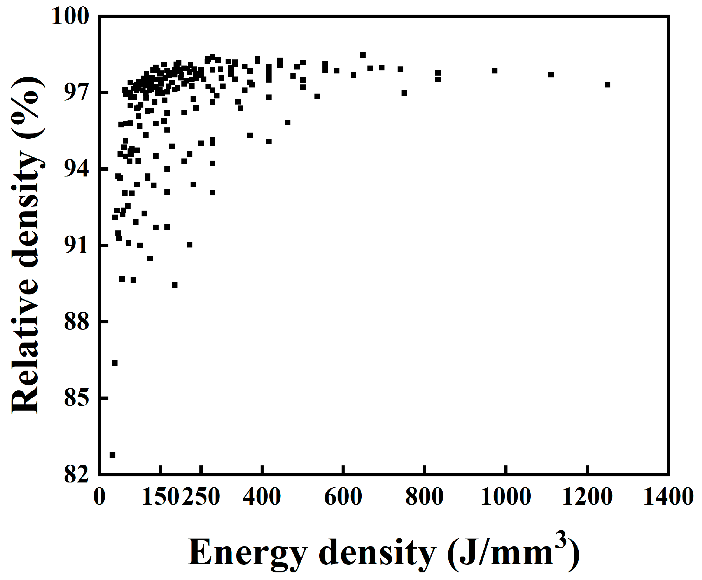
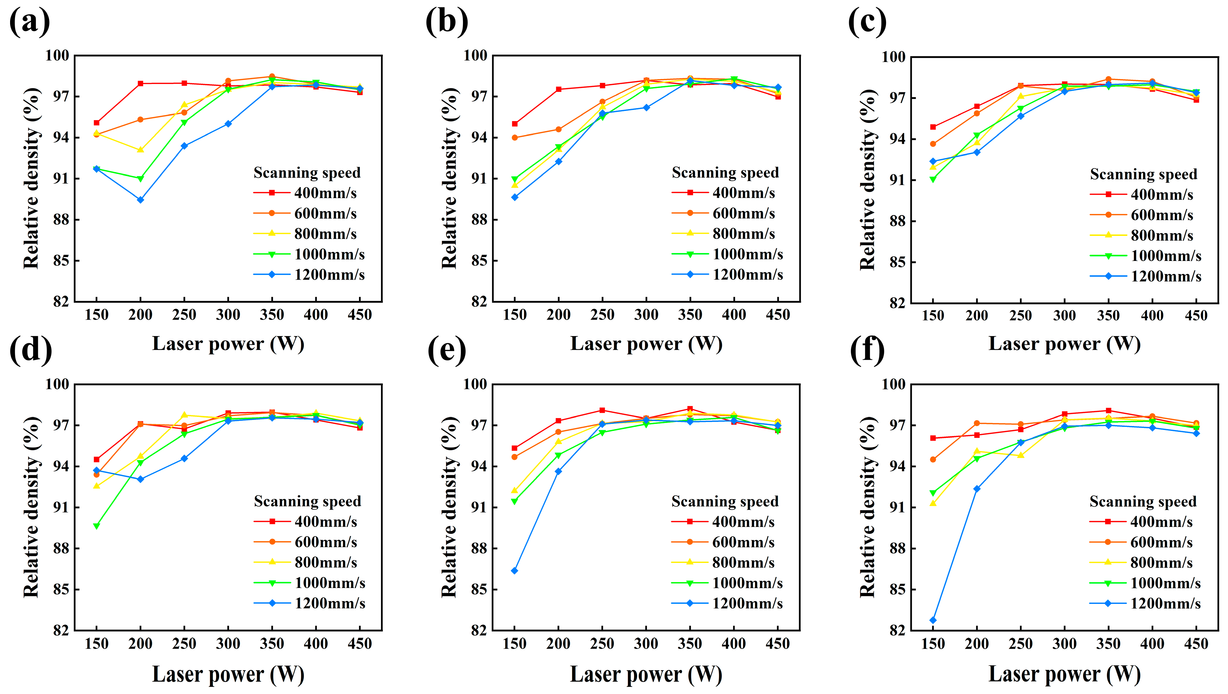
  • The main defects in the SLM forming process of the AlSi60 alloy include surface balling, lack of fusion, and porosity. Volumetric energy density is a key factor affecting forming, with well-formed samples obtainable within a process window of 150 J/mm3 to 250 J/mm3. However, volumetric energy density merely represents a simplification of the relationships between parameters such as laser power, scanning speed, and hatch spacing. The same volumetric energy density achieved through different combinations of process parameters can lead to variations in sample forming quality. Therefore, the further refined process window is: laser power of 300 W–350 W, scanning speed of 400 mm/s–800 mm/s, hatch spacing of 0.09 mm–0.13 mm, and volumetric energy density of 150 J/mm3 to 250 J/mm3.
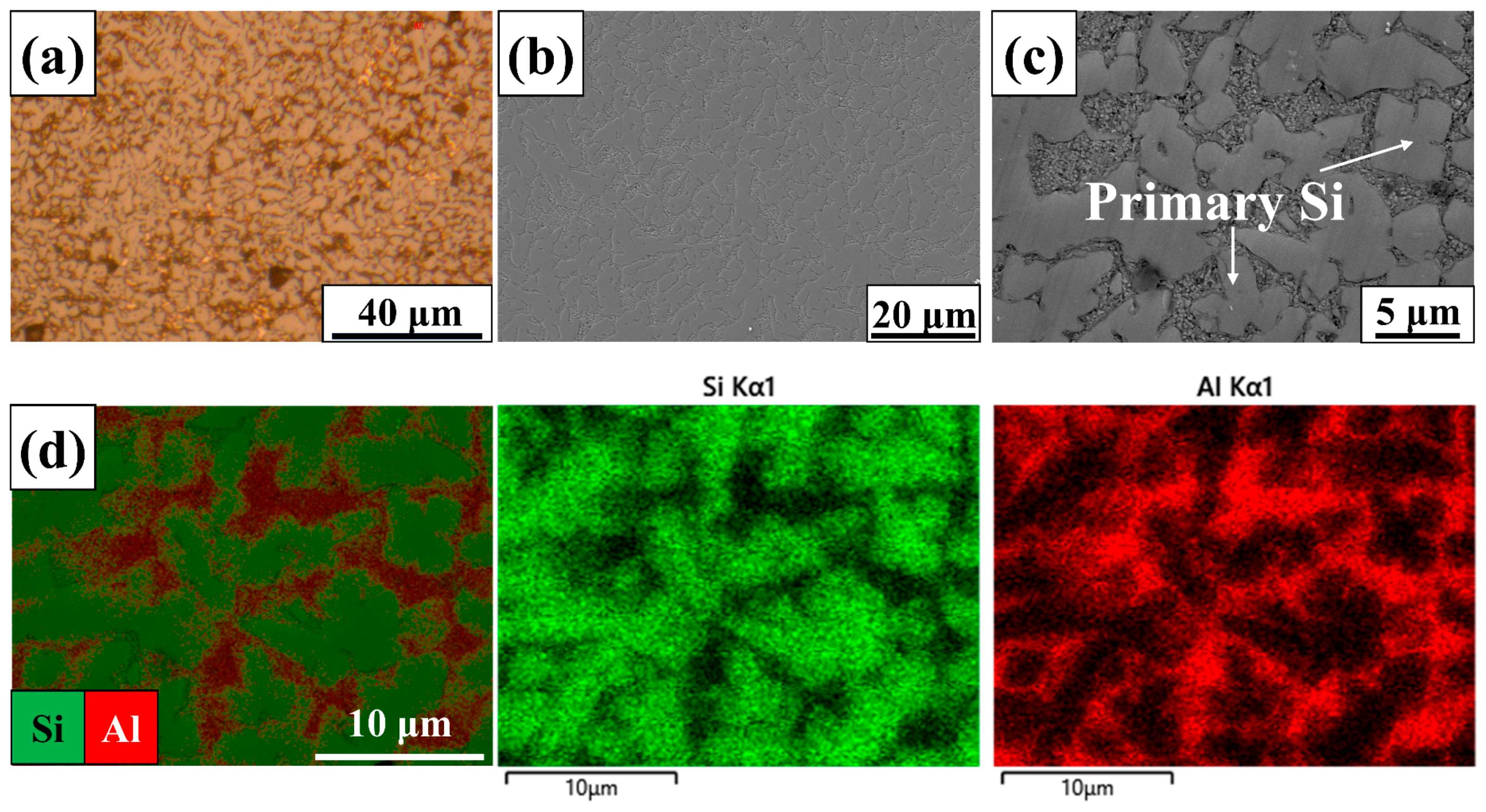
  • The SLM-formed AlSi60 alloy consists of primary Si, eutectic Si, and α-Al. The primary Si phase has sizes between 5 μm and 10 μm, characterized by sharp edges. The eutectic Si appears granular, about 0.5 μm in size, and is dispersed throughout the α-Al matrix.
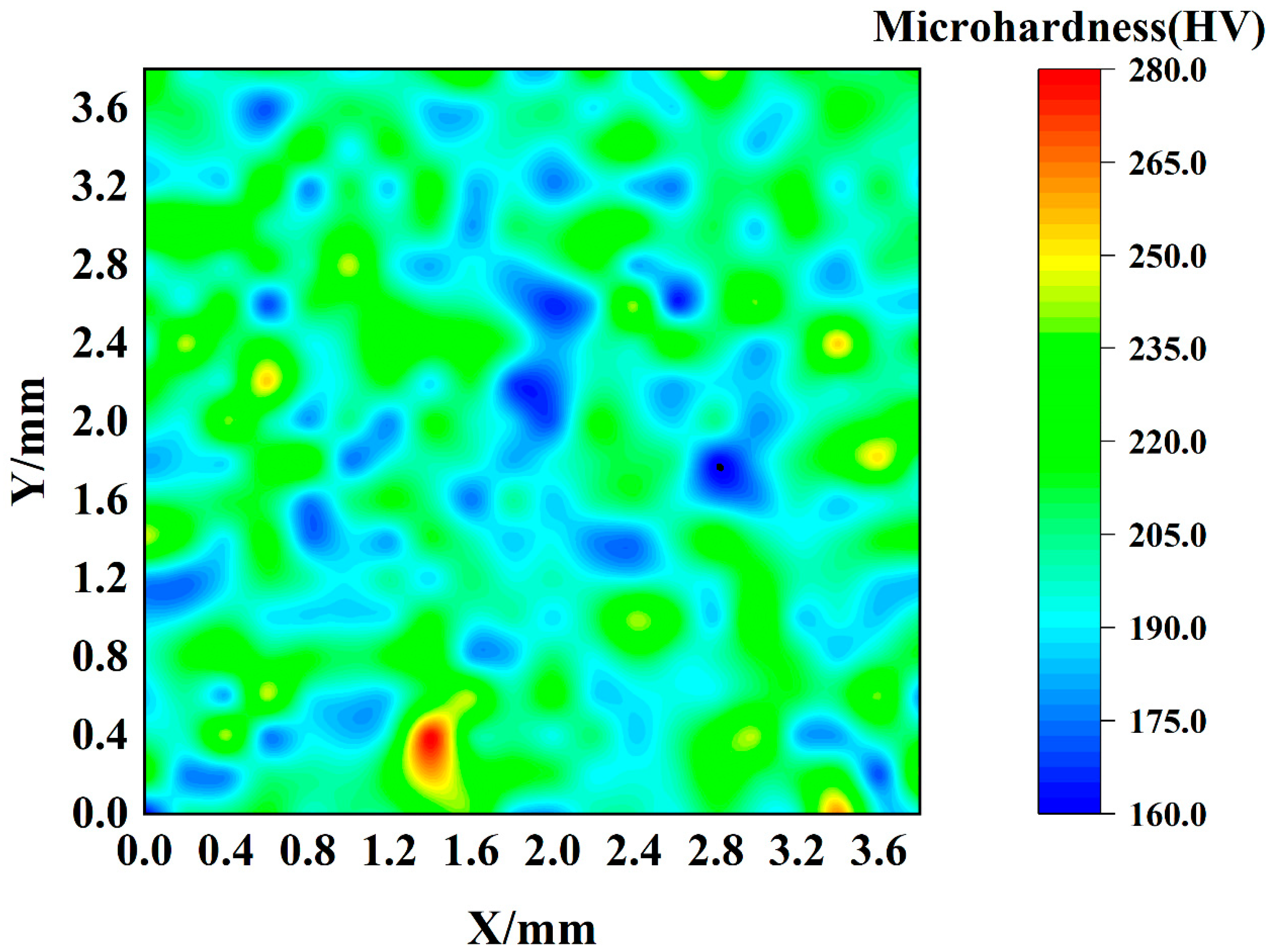
  • The SLM-formed AlSi60 alloy has an average hardness of 203 HV, higher than that of the AlSi60 alloy prepared by spray forming. The hardness values in the X and Y directions do not show significant anisotropy, due to the finer size and more uniform distribution of the primary Si phase prepared by SLM compared to other methods like spray forming.
  • The SLM-formed AlSi60 alloy samples have an average tensile strength of 219 MPa and an average elongation of 2.99%. During the tensile process, cracks initiated in the primary Si phase propagate throughout the entire Si phase and then extend to the Al matrix, where the Al matrix undergoes ductile fracture. Due to the high volume fraction of the Si phase, the tensile fracture is predominantly brittle, with only minor ductile fracture characteristics in the aluminum phase. This is why the tensile stress–strain curve exhibits only the elastic stage.

Author Contributions

Conceptualization, H.C. and Z.Z.; methodology, Z.Z. and G.Z.; software, Y.C. and P.R.; validation, G.L. and Y.H.; formal analysis, G.L.; investigation, S.M. and G.L.; resources, Z.Z., G.Z. and P.X.; data curation, Y.H. and G.L.; writing—original draft preparation, G.L.; writing—review and editing, Z.Z.; visualization, G.L. and Z.Z.; supervision, Z.Z.; project administration, H.C. and Z.Z.; funding acquisition, Z.Z.; All authors have read and agreed to the published version of the manuscript.

Funding

This work was financially supported by the National Natural Science Foundation of China (52205419), the National Key Research and Development Program (SQ2022YFB46002300), the Si-chuan Science and Technology Program (23ZDZX0013).

Institutional Review Board Statement

Not applicable.

Informed Consent Statement

Not applicable.

Data Availability Statement

The raw/processed data required to reproduce these findings cannot be shared at this time as the data also forms part of ongoing research.

Acknowledgments

We are also grateful to the Shiyanjia Lab (www.shiyanjia.com) for the SEM analysis.

Conflicts of Interest

Authors Yong Chen and Peng Rong were employed by the company AVIC Chengdu Aircraft Industrial (Group) Co., Ltd. The remaining authors declare that the research was conducted in the absence of any commercial or financial relationships that could be construed as a potential conflict of interest.

References

  1. Zhou, W.; Wang, R.-C.; Peng, C.-Q.; Cai, Z.-Y. Microstructure and properties of Al–Si functionally graded materials for electronic packaging. Trans. Nonferrous Met. Soc. China 2023, 33, 3583–3596. [Google Scholar] [CrossRef]
  2. Hogg, S.C.; Lambourne, A.; Ogilvy, A.; Grant, P.S. Microstructural characterisation of spray formed Si–30Al for thermal man-agement applications. Scr. Mater. 2006, 55, 111–114. [Google Scholar] [CrossRef]
  3. Xie, L.; Peng, C.; Wang, R.; Wang, X.; Cai, Z.; Liu, B. Research progress of high aluminum-silicon alloys in electronic packaging. Chin. J. Nonferrous Met. 2012, 22, 2578–2587. [Google Scholar]
  4. Dong, Y.; Lv, H. Research status and prospect of high silicon aluminum alloys. Light Alloy Fabr. Technol. 2021, 49, 11–16. [Google Scholar]
  5. Li, Q.; Xia, T.; Lan, Y.; Zhao, W.; Fan, L.; Li, P. Effect of rare earth cerium addition on the microstructure and tensile properties of hypereutectic Al–20%Si alloy. J. Alloys Compd. 2013, 562, 25–32. [Google Scholar] [CrossRef]
  6. Srirangam, P.; Kramer, M.; Shankar, S. Effect of strontium on liquid structure of Al–Si hypoeutectic alloys using high-energy X-ray diffraction. Acta Mater. 2011, 59, 503–513. [Google Scholar] [CrossRef]
  7. Wu, Y.; Wang, S.; Li, H.; Liu, X. A new technique to modify hypereutectic Al–24%Si alloys by a Si–P master alloy. J. Alloys Compd. 2009, 477, 139–144. [Google Scholar] [CrossRef]
  8. Hogg, S.C.; Atkinson, H.V. Inhibited coarsening of a spray-formed and extruded hypereutectic aluminum-silicon alloy in the semisolid state. Met. Mater. Trans. A 2005, 36, 149–159. [Google Scholar] [CrossRef]
  9. Qu, X.; Zhang, L.; Wu, M.; Ren, S. Review of metal matrix composites with high thermal conductivity for thermal man-agement applications. Prog. Nat. Sci. Mater. Int. 2011, 21, 189–197. [Google Scholar] [CrossRef]
  10. Liu, W.; Wang, R.; Peng, C.; Mo, J.; Zhu, X.W.; Peng, J. Research progress of spray deposited high Si-Al al-loys for electronic packaging. Chin. J. Nonferrous Met. 2012, 22, 3446–3455. [Google Scholar]
  11. Jia, Y.; Cao, F.; Ma, P.; Scudino, S.; Eckert, J.; Sun, J.; Wang, G. Microstructure and thermal conductivity of hypereutectic Al-high Si produced by casting and spray deposition. J. Mater. Res. 2016, 31, 2948–2955. [Google Scholar] [CrossRef]
  12. Zhao, Z.; Bo, L.; Li, L.; Huang, J. Status and Progress of Selective Laser Melting Forming Technology. Aeronaut. Manu-Facturing Technol. 2014, 57, 46–49. [Google Scholar] [CrossRef]
  13. Li, Y.; Gu, D. Parametric analysis of thermal behavior during selective laser melting additive manufacturing of aluminum alloy powder. Mater. Des. 2014, 63, 856–867. [Google Scholar] [CrossRef]
  14. Wang, M.; Zhu, H.; Qi, T.; Zhang, H.; Zeng, X. Selective laser melting Al-Si aluminum alloy and the crack formation mechanism. Laser Technol. 2016, 40, 219–222. [Google Scholar]
  15. Zhang, C.; Zhu, J.; Zheng, H.; Li, H.; Liu, S.; Cheng, G.J. A review on microstructures and properties of high entropy alloys manufactured by selective laser melting. Int. J. Extreme Manuf. 2020, 2, 032003. [Google Scholar] [CrossRef]
  16. Lu, J.; Lu, H.; Xu, X.; Yao, J.; Cai, J.; Luo, K. High-performance integrated additive manufacturing with laser shock peening–induced microstructural evolution and improvement in mechanical properties of Ti6Al4V alloy components. Int. J. Mach. Tools Manuf. 2020, 148, 103475. [Google Scholar] [CrossRef]
  17. Sheng, Z.; Ruizhi, G.; Qingsong, W.; Yusheng, S. Cracking Behavior and Formation Mechanism of TC4 Alloy Formed by Se-lective Laser Melting. J. Mech. Eng. 2013, 49, 21–27. [Google Scholar]
  18. Gao, P.; Huang, W.; Yang, H.; Jing, G.; Liu, Q.; Wang, G.; Wang, Z.; Zeng, X. Cracking behavior and control of β-solidifying Ti-40Al-9V-0.5 Y alloy produced by selective laser melting. J. Mater. Sci. Technol. 2020, 39, 144–154. [Google Scholar] [CrossRef]
  19. Duan, R.X.; Huang, B.Y.; Liu, Z.M.; Peng, K.; Lu, X.Q. Selective laser melting fabrication and cracking behavior of Rene104 nickel-based superalloy. Chin. J. Nonferrous Met. 2018, 28, 1568–1578. [Google Scholar]
  20. Zhang, J.; Li, S.; Wei, Q.; Shi, Y.; Wang, L.; Guo, L. Cracking Behavior and Inhibiting Process of Inconel 625 Alloy Formed by Selective Laser Melting. Chin. J. Rare Met. 2015, 39, 961–966. [Google Scholar]
  21. Kempen, K.; Vrancken, B.; Buls, S.; Thijs, L.; Van Humbeeck, J.; Kruth, J.-P. Selective Laser Melting of Crack-Free High Density M2 High Speed Steel Parts by Baseplate Preheating. J. Manuf. Sci. Eng. 2014, 136, 061026. [Google Scholar] [CrossRef]
  22. Zhang, W.; Zhu, H.; Hu, Z.; Zeng, X. Study on the Selective Laser Melting of AlSi10Mg. Acta Met. Sin. 2017, 53, 918–926. [Google Scholar]
  23. Aboulkhair, N.T.; Maskery, I.; Tuck, C.; Ashcroft, I.; Everitt, N.M. On the formation of AlSi10Mg single tracks and layers in selective laser melting: Microstructure and nano-mechanical properties. J. Am. Acad. Dermatol. 2016, 230, 88–98. [Google Scholar] [CrossRef]
  24. Kempen, K.; Thijs, L.; Van Humbeeck, J.; Kruth, J.-P. Mechanical Properties of AlSi10Mg Produced by Selective Laser Melting. Phys. Procedia 2012, 39, 439–446. [Google Scholar] [CrossRef]
  25. Prashanth, K.G.; Scudino, S.; Klauss, H.J.; Surreddi, K.B.; Löber, L.; Wang, Z.; Chaubey, A.K.; Kühn, U.; Eckert, J. Microstruc-ture and mechanical properties of Al–12Si produced by selective laser melting: Effect of heat treatment. Mater. Sci. Eng. A 2014, 590, 153–160. [Google Scholar] [CrossRef]
  26. Wang, X.; Zhang, L.; Fang, M.; Sercombe, T. The effect of atmosphere on the structure and properties of a selective laser melted Al–12Si alloy. Mater. Sci. Eng. A 2014, 597, 370–375. [Google Scholar] [CrossRef]
  27. Jia, Y.D.; Ma, P.; Prashanth, K.G.; Wang, G.; Yi, J.; Scudino, S.; Cao, F.Y.; Sun, J.F.; Eckert, J. Microstructure and thermal expan-sion behavior of Al-50Si synthesized by selective laser melting. J. Alloys Compd. 2017, 699, 548–553. [Google Scholar] [CrossRef]
  28. Kang, N.; Coddet, P.; Chen, C.; Wang, Y.; Liao, H.; Coddet, C. Microstructure and wear behavior of in-situ hypereutectic Al–high Si alloys produced by selective laser melting. Mater. Des. 2016, 99, 120–126. [Google Scholar] [CrossRef]
  29. Hanemann, T.; Carter, L.N.; Habschied, M.; Adkins, N.J.; Attallah, M.M.; Heilmaier, M. In-situ alloying of AlSi10Mg+Si using Selective Laser Melting to control the coefficient of thermal expansion. J. Alloys Compd. 2019, 795, 8–18. [Google Scholar] [CrossRef]
  30. Murray, J.L.; McAlister, A.J. The AI-Si (Aluminum-Silicon) System. Bull. Alloy Phase Diagr. 1984, 5, 74–84. [Google Scholar] [CrossRef]
  31. Wang, S.-R.; Ma, R.; Wang, Y.-Z.; Wang, Y.; Yang, L.-Y. Growth mechanism of primary silicon in cast hypoeutectic Al-Si alloys. Trans. Nonferrous Met. Soc. China 2012, 22, 1264–1269. [Google Scholar] [CrossRef]
  32. Wang, K.; Liu, Y.; Wang, J.; Li, Y. Influences of extrusion temperature on microstructure and properties of spray formed 60si40al alloy parts. Powder Metall. Ind. 2008, 18, 6–11. [Google Scholar]
  33. Xu, C.; Wang, H.; Liu, C.; Jiang, Q. Growth of octahedral primary silicon in cast hypereutectic Al–Si alloys. J. Cryst. Growth 2006, 291, 540–547. [Google Scholar] [CrossRef]
  34. Wang, R.-Y.; Lu, W.-H.; Hogan, L.M. Faceted growth of silicon crystals in Al-Si alloys. Met. Mater. Trans. A 1997, 28, 1233–1243. [Google Scholar] [CrossRef]
  35. Zhao, L.; Zhao, M.; Song, L.; Mazumder, J. Ultra-fine Al–Si hypereutectic alloy fabricated by direct metal deposition. Mater. Des. 2014, 56, 542–548. [Google Scholar] [CrossRef]
  36. Yamauchi, I.; Ohnaka, I.; Kawamoto, S.; Fukusako, T. Hot Extrusion of Rapidly Solidified Al–Si Alloy Powder by the Rotating-Water-Atomization Process. Trans. Jpn. Inst. Met. 1986, 27, 195–203. [Google Scholar] [CrossRef]
Figure 1. SEM images of pure Al powder, pure Si powder, and AlSi60 powder are (a), (b), and (c) respectively. (d) Particle size distribution of AlSi60 powder.
Coatings 14 00259 g001
Figure 2. (a) SLM experimental equipment and (b) SLM scanning strategy.
Coatings 14 00259 g002
Figure 3. Tensile specimen size.
Coatings 14 00259 g003
Figure 4. Effect of different volumetric energy densities on surface morphology: (a) 38 J/mm3, (b) 69 J/mm3, (c) 123 J/mm3, (d) 177 J/mm3, (e) 222 J/mm3, (f) 265 J/mm3.
Coatings 14 00259 g004
Figure 5. Effect of different volumetric energy densities on internal morphology: (a) 38 J/mm3, (b) 69 J/mm3, (c) 123 J/mm3, (d) 177 J/mm3, (e) 222 J/mm3, (f) 265 J/mm3.
Coatings 14 00259 g005
Figure 6. Effect of volumetric energy density on relative density.
Coatings 14 00259 g006
Figure 7. Influence of process parameters on forming densities: (a) fixed scanning spacing of 0.03 mm, (b) fixed scanning spacing of 0.05 mm, (c) fixed scanning spacing of 0.07 mm, (d) fixed scanning spacing of 0.09 mm, (e) fixed scanning spacing of 0.11 mm, (f) fixed scanning spacing of 0.13 mm.
Coatings 14 00259 g007
Figure 8. XRD patterns of SLM-formed AlSi60 alloy.
Coatings 14 00259 g008
Figure 9. Microstructural morphology of SLM-formed AlSi60 alloy: (a,b) are low-magnification metallography and SEM images, respectively; (c,d) represent high-magnification SEM images and EDS analysis.
Coatings 14 00259 g009
Figure 10. The TEM images of SLM-formed AlSi60: (a,b) morphology of AlSi60 under TEM, (c) high-resolution image of the area marked in (b). (df) Diffraction patterns of α-Al, primary Si phase, and eutectic Si, respectively.
Coatings 14 00259 g010
Figure 11. The microhardness distribution cloud map of SLM-formed AlSi60 alloy.
Coatings 14 00259 g011
Figure 12. Tensile stress–strain curves of SLM-formed AlSi60 alloy.
Coatings 14 00259 g012
Figure 13. Tensile fracture of SLM-formed AlSi60 alloy: (a,b) macroscopic morphology of the fracture, (c) cross-sectional morphology of the fracture, (d,e) high-magnification morphology of the fracture and EDS, (f) morphology of the plastic deformation area in the Al phase.
Coatings 14 00259 g013
Table 1. Optimal processing window for SLM forming of AlSi60 alloy.
Laser Power
(W)
Scanning Speed
(mm/s)
Hatch Spacing
(mm)
Volumetric Energy Density
(J/mm3)
300–350400–8000.09–0.13150–250
Table 2. Mechanical properties of SLM-formed AlSi60 alloys.
SampleTensile Strength
(MPa)
Elongation
(%)
12312.83
22092.69
32173.46
Disclaimer/Publisher’s Note: The statements, opinions and data contained in all publications are solely those of the individual author(s) and contributor(s) and not of MDPI and/or the editor(s). MDPI and/or the editor(s) disclaim responsibility for any injury to people or property resulting from any ideas, methods, instructions or products referred to in the content.

