
Silicon Dioxide Thin Films Deposited Using Oxide Targets: Results of Atomistic Simulation


Abstract
1. Introduction
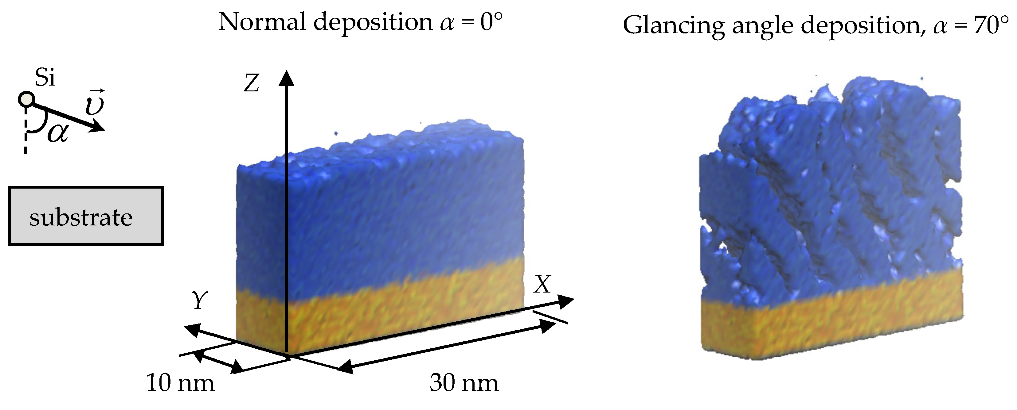
2. Methods
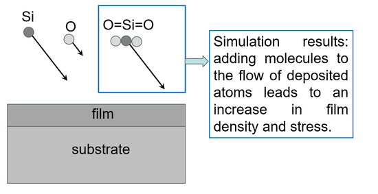
- Adding O=Si=O molecules, Si, and O atoms in a stoichiometric ratio of 1:2 to the upper part of the simulation box;
- MD modeling of the movement of these particles to the substrate and the formation of a structure on the surface of the substrate and previously deposited film layers;
- Removing particles reflected from the film surface from the simulation box;
- Increasing the vertical size of the simulation box by 0.01 nm to compensate for the increase in the thickness of the growing film.
3. Results and Discussion
4. Conclusions
Author Contributions
Funding
Institutional Review Board Statement
Informed Consent Statement
Data Availability Statement
Conflicts of Interest
References
- Tang, H.; Gao, J.; Zhang, J.; Wang, X.; Fu, X. Preparation and Spectrum Characterization of a High Quality Linear Variable Filter. Coatings 2018, 8, 308. [Google Scholar] [CrossRef]
- Qu, W.; Chen, Y.; Ma, C.; Peng, D.; Bai, X.; Zhao, J.; Liu, S.; Luo, L. Application of Optical Fiber Sensing Technology and Coating Technology in Blood Component Detection and Monitoring. Coatings 2024, 14, 173. [Google Scholar] [CrossRef]
- Barranco, A.; Borras, A.; Gonzalez-Elipe, A.R.; Palmero, A. Perspectives on Oblique Angle Deposition of Thin Films: From Fundamentals to Devices. Prog. Mater. Sci. 2016, 76, 59–153. [Google Scholar] [CrossRef]
- Raut, H.K.; Ganesh, V.A.; Nair, A.S.; Ramakrishna, S. Anti-Reflective Coatings: A Critical, in-Depth Review. Energy Environ. Sci. 2011, 4, 3779–3804. [Google Scholar] [CrossRef]
- Manenkov, A.A. Fundamental Mechanisms of Laser-Induced Damage in Optical Materials: Today’s State of Understanding and Problems. Opt. Eng. 2014, 53, 010901. [Google Scholar] [CrossRef]
- Angela Piegari, F.F. (Ed.) Optical Thin Films and Coatings; Elsevier: Amsterdam, The Netherlands, 2018. [Google Scholar]
- Greene, J.E. Review Article: Tracing the Recorded History of Thin-Film Sputter Deposition: From the 1800s to 2017. J. Vac. Sci. Technol. A 2017, 35, 05C204. [Google Scholar] [CrossRef]
- Mateev, M.; Lautenschläger, T.; Spemann, D.; Finzel, A.; Gerlach, J.W.; Frost, F.; Bundesmann, C. Systematic Investigation of the Reactive Ion Beam Sputter Deposition Process of SiO2. Eur. Phys. J. B 2018, 91, 45. [Google Scholar] [CrossRef]
- Tolenis, T.; Grinevičiūtė, L.; Smalakys, L.; Ščiuka, M.; Drazdys, R.; Mažulė, L.; Buzelis, R.; Melninkaitis, A. Next Generation Highly Resistant Mirrors Featuring All-Silica Layers. Sci. Rep. 2017, 7, 10898. [Google Scholar] [CrossRef]
- Bernstein, J.; Gerlach, J.W.; Finzel, A.; Bundesmann, C. Ion Beam Sputter Deposition of SiO2 thin Films Using Oxygen Ions. Eur. Phys. J. B 2022, 95, 39. [Google Scholar] [CrossRef]
- He, X.; Wu, J.; Li, X.; Gao, X.; Zhao, L.; Wu, L. Synthesis and Properties of Silicon Dioxide Films Prepared by Pulsed Laser Deposition Using Ceramic SiO2 Target. Appl. Surf. Sci. 2009, 256, 231–234. [Google Scholar] [CrossRef]
- Bhatt, V.; Chandra, S. Silicon Dioxide Films by RF Sputtering for Microelectronic and MEMS Applications. J. Micromech. Microeng. 2007, 17, 1066. [Google Scholar] [CrossRef]
- Fogarassy, E.; Slaoui, A.; Fuchs, C.; Stoquert, J.P. Deposition of SiO2 by Reactive Excimer Laser Ablation from a SiO Target. Appl. Surf. Sci. 1990, 46, 195–199. [Google Scholar] [CrossRef]
- Telesh, E.V.; Dostanko, A.P.; Gurevich, O. V Stoichiometry of Silicon Dioxide Films Obtained by Ion-Beam Sputtering. J. Appl. Spectrosc. 2018, 85, 67–72. [Google Scholar] [CrossRef]
- Ristau, D.; Gross, T. Ion Beam Sputter Coatings for Laser Technology. In Proceedings of the Optical Systems Design 2005, Jena, Germany, 13–15 September 2005; SPIE: Bellingham, WA, USA, 2005; Volume 5963, p. 596313. [Google Scholar]
- Kim, D.-H.; Lee, G.-H.; Yup Lee, S.; Hyun Kim, D. Atomic Scale Simulation of Physical Sputtering of Silicon Oxide and Silicon Nitride Thin Films. J. Cryst. Growth 2006, 286, 71–77. [Google Scholar] [CrossRef]
- Grigoriev, F.V.; Sulimov, A.V.; Kochikov, I.; Kondakova, O.A.; Sulimov, V.B.; Tikhonravov, A.V. High-Performance Atomistic Modeling of Optical Thin Films Deposited by Energetic Processes. Int. J. High Perform. Comput. Appl. 2014, 29, 184–192. [Google Scholar] [CrossRef]
- Grigoriev, F.V.; Sulimov, A.V.; Katkova, E.V.; Kochikov, I.V.; Kondakova, O.A.; Sulimov, V.B.; Tikhonravov, A.V. Computational Experiments on Atomistic Modeling of Thin Film Deposition. Appl. Opt. 2017, 56, C87–C90. [Google Scholar] [CrossRef]
- Hawkeye, M.M.; Brett, M.J. Glancing Angle Deposition: Fabrication, Properties, and Applications of Micro- and Nanostructured Thin Films. J. Vac. Sci. Technol. A Vac. Surf. Film. 2007, 25, 1317. [Google Scholar] [CrossRef]
- Grigoriev, F.V.; Sulimov, V.B.; Tikhonravov, A.V. Atomistic Simulation of Stresses in Growing Silicon Dioxide Films. Coatings 2020, 10, 220. [Google Scholar] [CrossRef]
- Taguchi, M.; Hamaguchi, S. MD Simulations of Amorphous SiO2 Thin Film Formation in Reactive Sputtering Deposition Processes. Thin Solid Films 2007, 515, 4879–4882. [Google Scholar] [CrossRef]
- Badorreck, H.; Steinecke, M.; Jensen, L.; Ristau, D.; Jupé, M.; Müller, J.; Tonneau, R.; Moskovkin, P.; Lucas, S.; Pflug, A.; et al. Correlation of Structural and Optical Properties Using Virtual Materials Analysis. Opt. Express 2019, 27, 22209–22225. [Google Scholar] [CrossRef]
- Grigoriev, F.V.; Sulimov, A.V.; Katkova, E.V.; Kochikov, I.V.; Kondakova, O.A.; Sulimov, V.B.; Tikhonravov, A.V. Full-Atomistic Nanoscale Modeling of the Ion Beam Sputtering Deposition of SiO2 Thin Films. J. Non. Cryst. Solids 2016, 448, 1–5. [Google Scholar] [CrossRef]
- Berendsen, H.J.C.; Postma, J.P.M.; Van Gunsteren, W.F.; Dinola, A.; Haak, J.R. Molecular Dynamics with Coupling to an External Bath. J. Chem. Phys. 1984, 81, 3684–3690. [Google Scholar] [CrossRef]
- Abraham, M.J.; Murtola, T.; Schulz, R.; Páll, S.; Smith, J.C.; Hess, B.; Lindahl, E. GROMACS: High Performance Molecular Simulations through Multi-Level Parallelism from Laptops to Supercomputers. SoftwareX 2015, 1, 19–25. [Google Scholar] [CrossRef]
- Humphrey, W.; Dalke, A.; Schulten, K. VMD: Visual Molecular Dynamics. J. Mol. Graph. 1996, 14, 33–38. [Google Scholar] [CrossRef]
- Voevodin, V.V.; Antonov, A.S.; Nikitenko, D.A.; Shvets, P.A.; Sobolev, S.I.; Sidorov, I.Y.; Stefanov, K.S.; Voevodin, V.V.; Zhumatiy, S.A. Supercomputer Lomonosov-2: Large Scale, Deep Monitoring and Fine Analytics for the User Community. Supercomput. Front. Innov. 2019, 6, 4–11. [Google Scholar]
- Schmidt, M.W.; Baldridge, K.K.; Boatz, J.A.; Elbert, S.T.; Gordon, M.S.; Jensen, J.H.; Koseki, S.; Matsunaga, N.; Nguyen, K.A.; Su, S.; et al. General Atomic and Molecular Electronic Structure System. J. Comput. Chem. 1993, 14, 1347–1363. [Google Scholar] [CrossRef]
- Hofsäss, H.; Zhang, K.; Mutzke, A. Simulation of Ion Beam Sputtering with SDTrimSP, TRIDYN and SRIM. Appl. Surf. Sci. 2014, 310, 134–141. [Google Scholar] [CrossRef]
- Begou, T.; Lumeau, J. Accurate Analysis of Mechanical Stress in Dielectric Multilayers. Opt. Lett. 2017, 42, 3217–3220. [Google Scholar] [CrossRef]
- Abadias, G.; Chason, E.; Keckes, J.; Sebastiani, M.; Thompson, G.B.; Barthel, E.; Doll, G.L.; Murray, C.E.; Stoessel, C.H.; Martinu, L. Review Article: Stress in Thin Films and Coatings: Current Status, Challenges, and Prospects. J. Vac. Sci. Technol. A 2018, 36, 20801. [Google Scholar] [CrossRef]
- Vedam, K.; Limsuwan, P. Piezo- and Elasto-optic Properties of Liquids under High Pressure. II. Refractive Index vs Density. J. Chem. Phys. 1978, 69, 4772–4778. [Google Scholar] [CrossRef]
- Melninkaitis, A.; Grinevičiūtė, L.; Abromavičius, G.; Mažulė, L.; Smalakys, L.; Pupka, E.; Ščiuka, M.; Buzelis, R.; Kičas, S. Next-Generation All-Silica Coatings for UV Applications. In Proceedings of the Laser-Induced Damage in Optical Materials 2017, Colorado, CO, USA, 24–27 September 2017; SPIE: Bellingham, WA, USA, 2017; Volume 10447. [Google Scholar]
- Grigoriev, F.V.; Sulimov, V.B.; Tikhonravov, A.V. Atomistic Simulation of the Glancing Angle Deposition of SiO2 Thin Films. J. Non Cryst. Solids 2019, 512, 98–102. [Google Scholar] [CrossRef]
- Tait, R.N.; Smy, T.; Brett, M.J. Modelling and Characterization of Columnar Growth in Evaporated Films. Thin Solid Films 1993, 226, 196–201. [Google Scholar] [CrossRef]


| Method | R(Si-O), nm | α(O-Si-O), grad | Charge |
|---|---|---|---|
| QC | 0.149 | 180 | 0 |
| FF | 0.155 | 180 | 0 |
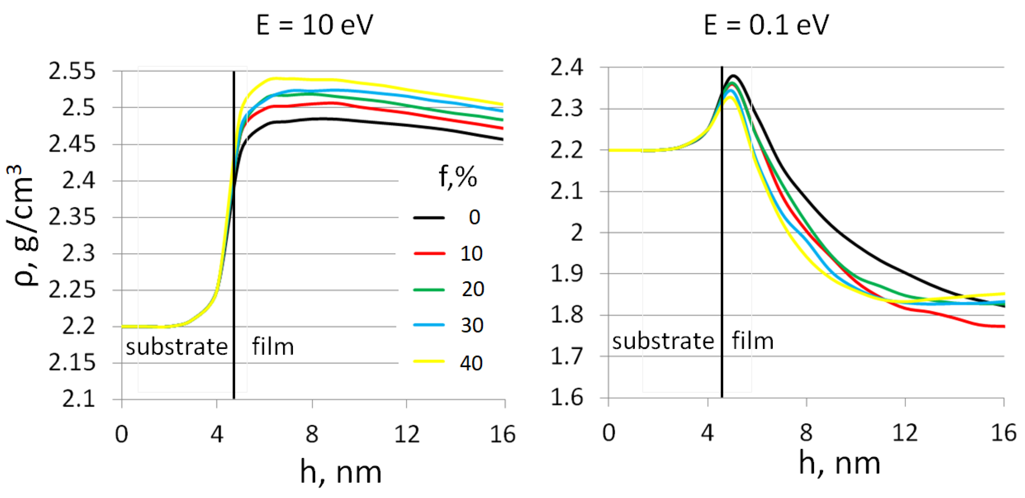
| f, % | 0 | 10 | 20 | 30 | 40 | 50 |
|---|---|---|---|---|---|---|
| |σxx| | 117 | 133 | 152 | 160 | 162 | 165 |
| |σyy| | 122 | 138 | 140 | 148 | 162 | 170 |
Disclaimer/Publisher’s Note: The statements, opinions and data contained in all publications are solely those of the individual author(s) and contributor(s) and not of MDPI and/or the editor(s). MDPI and/or the editor(s) disclaim responsibility for any injury to people or property resulting from any ideas, methods, instructions or products referred to in the content. |
© 2024 by the authors. Licensee MDPI, Basel, Switzerland. This article is an open access article distributed under the terms and conditions of the Creative Commons Attribution (CC BY) license (https://creativecommons.org/licenses/by/4.0/).
Share and Cite
Grigoriev, F.V.; Sulimov, V.B.; Tikhonravov, A.V. Silicon Dioxide Thin Films Deposited Using Oxide Targets: Results of Atomistic Simulation. Coatings 2024, 14, 258. https://doi.org/10.3390/coatings14030258
Grigoriev FV, Sulimov VB, Tikhonravov AV. Silicon Dioxide Thin Films Deposited Using Oxide Targets: Results of Atomistic Simulation. Coatings. 2024; 14(3):258. https://doi.org/10.3390/coatings14030258
Chicago/Turabian StyleGrigoriev, F. V., V. B. Sulimov, and A. V. Tikhonravov. 2024. "Silicon Dioxide Thin Films Deposited Using Oxide Targets: Results of Atomistic Simulation" Coatings 14, no. 3: 258. https://doi.org/10.3390/coatings14030258
APA StyleGrigoriev, F. V., Sulimov, V. B., & Tikhonravov, A. V. (2024). Silicon Dioxide Thin Films Deposited Using Oxide Targets: Results of Atomistic Simulation. Coatings, 14(3), 258. https://doi.org/10.3390/coatings14030258