1. Introduction
Gallium oxide (Ga
2O
3), as an ultrawide bandgap semiconductor, has numerous potential applications in the fields of electronics and optoelectronics. It is a promising material for transistors and rectifiers in high-power electronics [
1,
2], as well as for solar-blind UV photodetectors and photodiodes [
1,
2,
3]. In addition, as was recently demonstrated, it can also be utilized in gas-sensing applications [
4].
Several processing techniques, from bulk growth methods to thin-film formation procedures, have been developed to synthesize Ga
2O
3 [
1,
2,
5]. Among the film formation techniques, molecular beam epitaxy [
6], metal–organic chemical vapor deposition [
7], halide vapor phase epitaxy [
8], pulsed laser deposition [
9], mist-chemical vapor deposition [
9], and sputtering [
5] are the most commonly used methods. Sputtering is a frequently used technique, mainly because it offers the possibility of depositing highly uniform layers at low temperatures [
10,
11,
12]. Ga
2O
3 films prepared in this way have demonstrated the potential to be used as a material in solar-blind UV photodetectors [
3,
13,
14]. Sputtering can be carried out under different deposition conditions/parameters. These have a significant influence on the properties of the films [
5,
15], and also enable the control of these properties. For the deposition of gallium oxide, most often, a ceramic Ga
2O
3 target is used. As it is non-conductive, a radio frequency power source should be utilized. Sputtering such a Ga
2O
3 target in an Ar atmosphere usually leads to oxygen-deficient films [
16,
17]. Hence, in many cases, an Ar + O
2 atmosphere is used during deposition [
14,
15,
18,
19,
20]. The investigations on the reactive sputtering of Ga targets are scarce, mainly due to the low melting point (T
m = 30 °C) of gallium. Only one recent study could be found on the preparation of Ga
2O
3 films using the reactive sputtering of liquid Ga [
21].
The aim of this work was to study the sputtering process of a liquid Ga target during the deposition of gallium oxide films. The modeling of the reactive sputtering process was carried out based on the Berg model [
22,
23]. The sputtering parameters, such as the partial sputtering yields and the sticking coefficient, were determined. The dependence of the composition and the refractive index of the deposited films on the sputtering conditions was also investigated. Finally, a comparison between the deposition of gallium oxide from a liquid Ga target and ceramic Ga
2O
3 targets was performed.
2. Materials and Methods
2.1. Sample Preparation
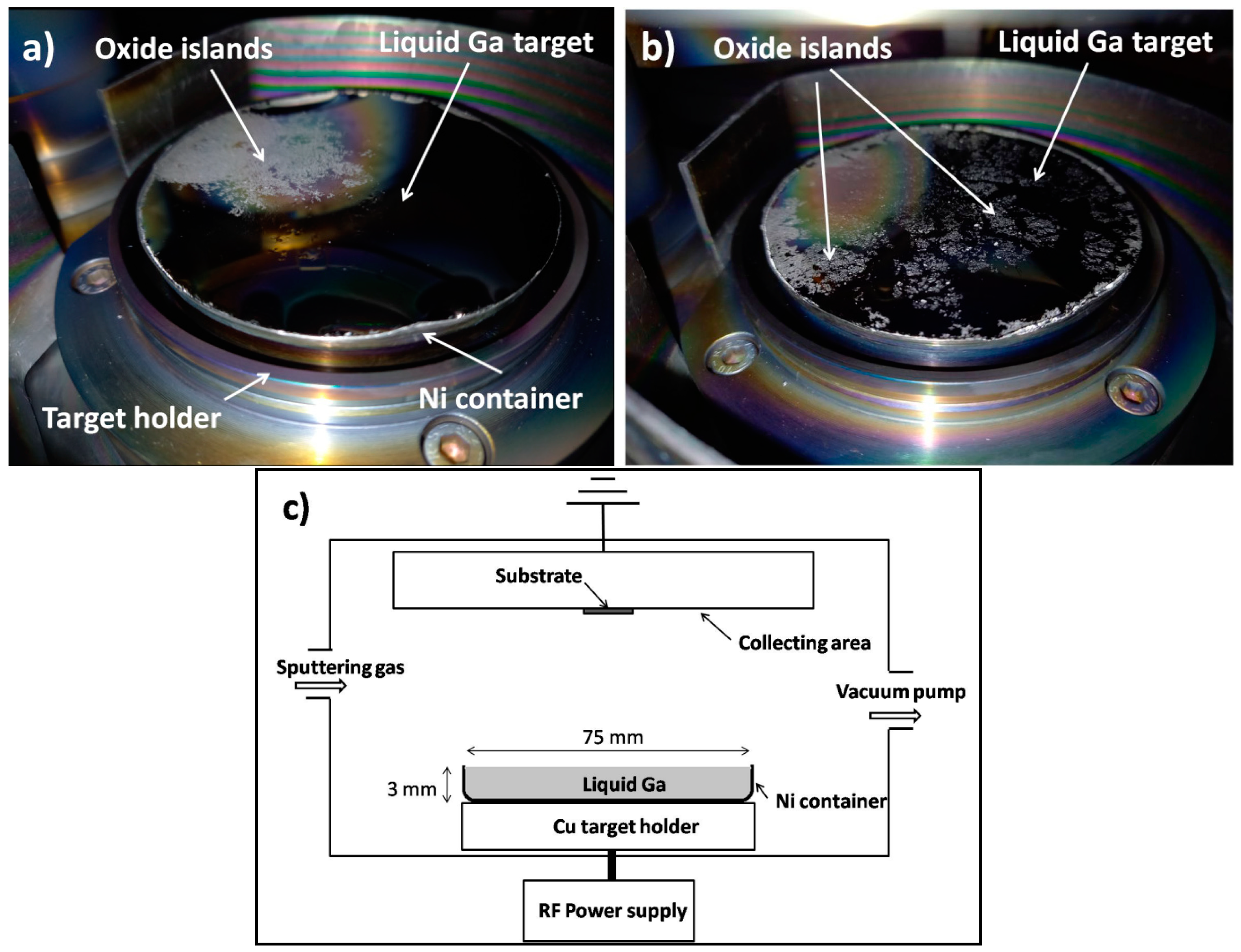
The high-purity gallium (Alusuisse, purity 99.9999%) was placed on the lower target area of a Leybold Z400 RF sputtering device, in a circular crucible fabricated from a 0.2 mm Ni plate (see
Figure 1). The diameter of the container was 75 mm, and the height of its side wall was about 3 mm. This shape fitted well on the copper target holder of the sputtering device, which was water-cooled, and ensured the coupling of the RF power.
The 3 mm wall height ensured that the relatively small amount of Ga, which is liquid at 30 °C, but was mostly supercooled during the manipulations, completely covered the diameter of the 75 mm target. The target was in a liquid state during sputtering, as verified through visual inspection. Due to the high surface tension of Ga in the Ni container, and the moderate wettability of the Ni interface, it easily breaks up into islands. To avoid this, we used a technique (the so-called fluxless oxide remover) similar to active soldering. The mechanical activation required to remove the oxide layer from the Ni surface can be performed with a brush (e.g., a stainless wire brush or steel spatula) or via ultrasonic vibration. In our case, the wall of the container was heated from the outside with an electric heater to 350 °C under ambient conditions, while the Ni surface in contact with the Ga melt was scraped with a steel spatula, until a continuous surface covered with the melt was obtained (at least 15 min of mechanical activation).
The liquid Ga target was reactively sputtered using the above-mentioned Leybold Z400 RF sputtering device, operated at a frequency of 13.56 MHz. The reason for our choosing this device was that it has a bottom target holder, which is necessary for the liquid target. However, this experiment can also be performed using pulsed DC sputtering or HiPIMS devices equipped with a bottom target placement option, as well. For all deposition experiments, the sputtering chamber was evacuated, to achieve a base pressure of 4 × 10⁻⁴ Pa. Oxygen was admitted to the deposition chamber through a flow controller. Oxygen flows of 6, 9, 12, 20, 26, and 32 sccm (standard cubic centimeter per minute) were used. These flow rates approximately correspond to 3.5, 5, 6.8, 11.3, 15, and 19 × 10−2 Pa gas pressures in non-sputtering conditions (the actual values were measured before each sputtering experiment). The film deposition was carried out using a mixture of O2 and Ar gases at a total pressure of 2 Pa. The DC target potential that developed on the cathode during sputtering was kept constant via adjustment of the RF power. Three sets of samples were prepared using the DC target potentials of 1200 V, 1300 V, and 1400 V (corresponding to about 53 W, 65 W, and 70 W of RF power, respectively). The deposition time was 30 min for 1300 V and 1400 V, while it was 40 min for the 1200 V DC target potential. The target-to-substrate distance was about 50 mm, and the substrate holder was neither cooled nor heated during sputtering. For comparison purposes, a film was also deposited using a ceramic Ga2O3 target (Kurt J. Lesker, purity 99.99%). The sputtering of this reference sample was carried out at 1400 V (80 W) for 30 min, using 2 Pa Ar pressure. In all cases, the substrate was a piece of Si (100) single-crystal wafer.
2.2. Characterization
The structure of the films was investigated via X-ray diffraction (XRD), using a D8 Discover X-ray diffractometer (Bruker AXS, Karlsruhe, Germany) equipped with a Göbel mirror and a scintillation detector. The measurements were performed in parallel beam geometry between 15° and 90° of 2θ with Cu-Kα radiation. The X-ray beam dimension was 1 mm × 5 mm, while the 2θ step size and the scan speed were 0.02° and 2.5 s/step, respectively. The surface features of the samples were studied via scanning electron microscopy (SEM), using a Scios 2 dual-beam scanning electron microscope. Compositional variations were examined via backscattered electrons, and also via energy-dispersive spectroscopy (EDS). The EDS measurements were carried out on a 65 µm × 43 µm area, using an electron beam with 4.2 keV energy and 3.2 nA current. The error of composition, i.e., the error of the value x in Ga2Ox, was ±0.38.
The composition of a sputtered layer was also determined via X-ray photoelectron spectroscopy (XPS), using Ecalab Xi+ equipment (Thermo Fisher Scientific, Waltham, MA, USA). The 1 cm-sized piece of sample was fixed with carbon sticking tape to the sample holder, and mounted to the UHV condition (1 × 10⁻⁸ Pa). As the “as received” state of the sample showed some organic contamination, which is usual for surfaces arriving from the free air condition, the sample was gradually cleaned in further steps, and checked between them. Avoiding damage to the layer beneath, possibly generated by the usual Ar+ beam sputtering, a mild Ar cluster beam was applied, to remove the adsorbed molecules such as carbohydrates, instead. The weak impact of the setup used (1000 atom clusters at 2 keV = >2 eV/atom) ensured that neither compositional nor chemical state changes took place via the cleaning procedure. The measured spot was chosen to be relatively large (900 µm), for good spectrum statistics. Spectra were detected at three different locations at an 0.6 eV energy resolution, with a 0.1 eV step size. The measured XPS spectra included the following peaks: Ga 2p 3/2 and 1/2 (1119 eV and 1146 eV), O 1 s (532 eV), and C 1 s 284 eV. The spectra were evaluated via determining the peak area. After the application of the usual Shirley background subtraction, the peak intensities were derived via Gaussian–Lorentzian fitting for the peak shapes. The component concentration was calculated with sensitivity factors from the ALTHERMO1 library, assuming a homogeneous distribution of components.
The ellipsometric measurements were carried out on the specimens using a WOOLLAM M2000U spectroscopic ellipsometer in the 190–1690 nm range, at an incidence of 70°. The evaluation of the data and the determination of the layer thickness and refractive index of the samples were performed using the CompleteEase software (version number is 5.15). The layers were modeled using the Tauc–Lorentz oscillator [
24]. The thickness of the films using the above-described preparation conditions is in the range of 160 nm and 460 nm for the Ga target, and 160 nm for the ceramic target.
2.3. Model of Reactive Sputtering
The determination of the sputtering yields, i.e., the average number of sputtered atoms per incoming ion and the sticking coefficient, defined as the probability that an incoming neutral reactive gas molecule reacts with an unreacted metal atom at the surface, was carried out based on the Berg model. The original Berg model offers a relatively simple, analytical approach to describing the reactive sputtering process [
22]. However, in some cases, the assumptions applied in the Berg model cannot adequately describe the reactive sputtering process; hence, an upgrade was introduced [
23]. The upgraded Berg model includes additional mechanisms for the formation of the compound (besides chemisorption) on the target surface and subsurface; these are the direct implantation of reactive gas ions and the knock-in of already chemisorbed reactive gas atoms via the impact of Ar ions. The model assumes one surface layer on the target (which is not a monolayer) that incorporates all reactive gas atoms (either chemisorbed or implanted); this layer is also assumed to have a constant composition. The other important change compared to the original model consists of the assumption of the atomic sputtering of the compound, and the introduction of atomic sputtering yields. Next, a short summary of this upgraded model will be given.
Assuming a uniform partial pressure across the sputtering chamber, the flux of reactive gas molecules arriving to all the surfaces can be given according to the kinetic gas theory:
where
p is the reactive gas partial pressure,
k is the Boltzmann constant,
T is the temperature in the chamber, and
m is the mass of the reactive gas molecule, respectively.
In the steady state, the compound formation and removal are in equilibrium at the target, resulting in a constant surface coverage (
θt). The balance equation for the target can be given as [
23]:
where
J is the ion current density, which is assumed to be uniformly distributed over the target surface;
q is the elementary charge; and
Yk and
Yc are the knock-in yield and the partial sputtering yield of the reactive gas atoms in the compound, respectively.
αt is the sticking coefficient of the target;
αi is the probability that a reactive gas ion is implanted in the target;
ptot denotes the total pressure in the deposition chamber; and
z represents the compound stoichiometry, i.e.,
z = 3/2 for Ga
2O
3. It was assumed that oxygen and argon have the same ionization probability.
The surface coverage for the collecting area (
θc), which is the net result of the material deposition from the target and the formation of the compound at the collecting surface, can also be defined. In the steady state, the corresponding balance equation can be given as:
where
αc is the sticking coefficient of the reactive gas on the collecting area;
Ac and
At are the surface area of the collecting surface and the target, respectively; and
Ymc and
Ymm are the partial sputtering yield of the metal in the compound and the sputtering yield of the unreacted metal, respectively.
Based on the above-described model, one can calculate the amount of deposited material. It is assumed that the deposited film only contains stoichiometric oxide, with a fraction of
θc, and pure metal with a fraction of (1 −
θc).
θt and
θc can be expressed using Equations (2) and (3). Thus, the thickness of the deposited layer can be given as follows:
where
Mm (
Mc) and
ρm (
ρc) are the molar mass and the density of the metal (compound), respectively;
t is the duration of the deposition; and
N is the Avogadro number. Note that the second term in the parenthesis is divided by 2, as a Ga
2O
3 molecule contains two gallium atoms.
Via deposition using different reactive gas flows, and by measuring the thickness of the forming layers, one can determine the sputtering yields of the target materials and the sticking coefficients. In our calculations, it is assumed that the sticking coefficients on the target and the collecting area are equal (
αt =
αc =
α), and that the reactive gas ions implanted in the subsurface have a sticking probability of unity (
αi = 1). The current density was calculated based on the DC target potential, the sputtering power, and the surface area of the target (
At = 44 cm
2). The temperature in the deposition chamber was estimated to be 330 K, based on an earlier study [
25]. The collecting area (
Ac = 115 cm
2) was determined via measuring the area of the deposition pattern inside the sputtering chamber. The material was assumed to be uniformly deposited on the collecting area.
3. Results and Discussion
Figure 2 presents a typical example of the XRD pattern of the sputtered films. No crystalline peaks can be found, except the reflections of the Si substrate. Similar results were obtained for other samples, as well, regardless of the deposition conditions. Thus, the films in this work can be identified as X-ray-amorphous, as is often the case for RF sputtered films deposited at room temperature [
5,
11,
15].
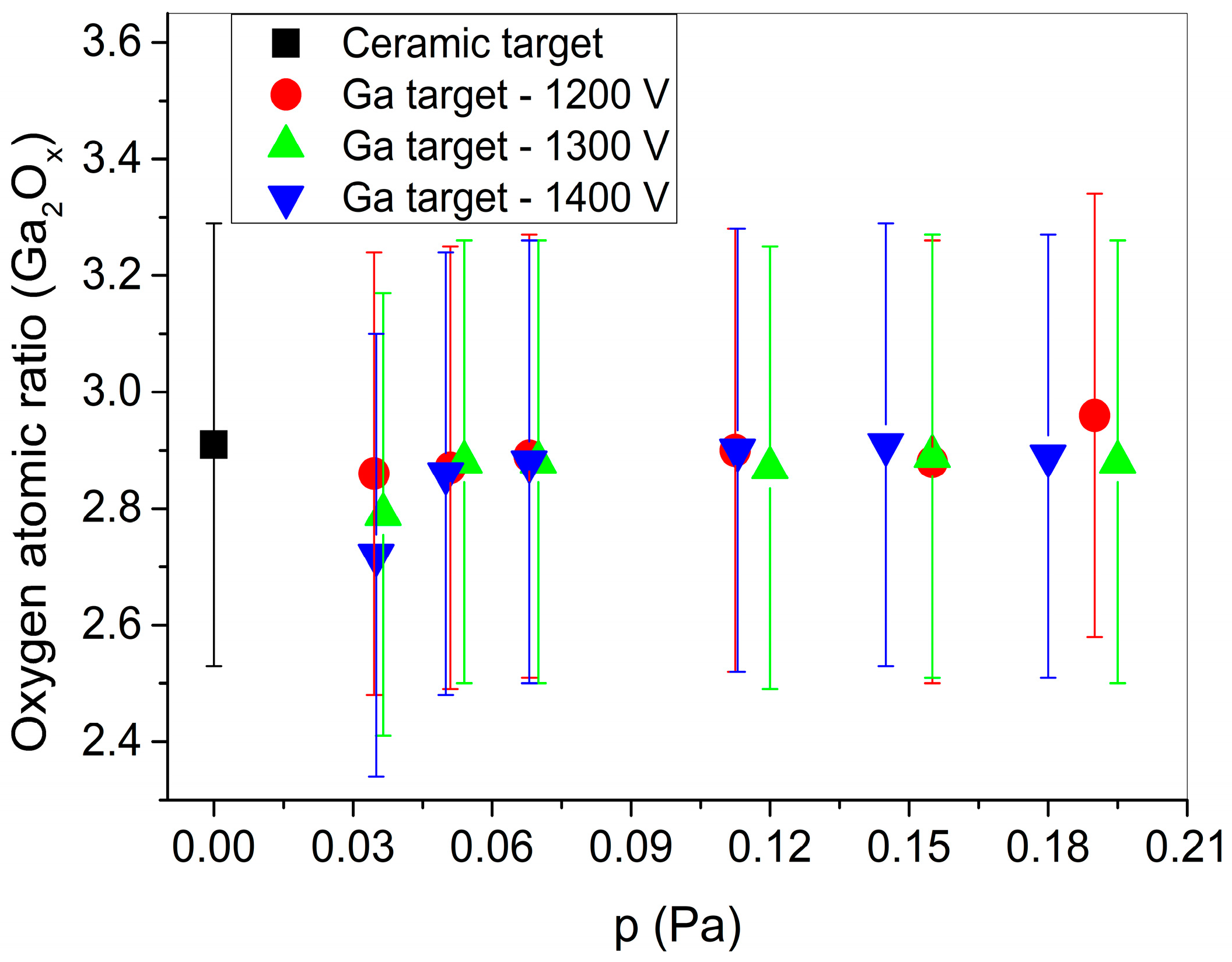
The oxygen content of the sputtered films, measured via EDS, is shown in
Figure 3 as a function of the oxygen partial pressure (detailed EDS results can also be found in
Tables S1–S3 of the Supplementary Materials). The measurements confirm that a gallium oxide layer can be grown via reactive sputtering, using a liquid gallium target. The oxygen content of the films is slightly below the nominal Ga
2O
3 stoichiometry value, even for the highest applied oxygen flow. Nevertheless, the sample sputtered using 1200 V and 32 sccm of oxygen (0.19 Pa of O
2 pressure) presents a higher O/Ga atomic ratio than a non-reactively sputtered gallium oxide film grown using a ceramic Ga
2O
3 target. As shown in
Figure 3, increasing the oxygen partial pressure results in only slight changes in the oxygen content. A small effect of the DC target potential in the composition of the Ga
2O
x films can be seen only for the lowest oxygen pressures; i.e., an increase in the DC target potential decreases the oxygen content of the layers.
For reference, the composition of the sample prepared at 1300 V and 32 sccm (0.19 Pa of O
2 pressure) was also measured via XPS.
Figure 4 shows the recorded spectrum, including the main peaks of Ga and O. No elements other than gallium and oxygen were observed on the cleaned surface. The calculated concentration of Ga at the three measured positions was identical within 1%, which resulted in X = 2.76 after its conversion to Ga
2O
x form. It confirms the EDS data within the expected error.
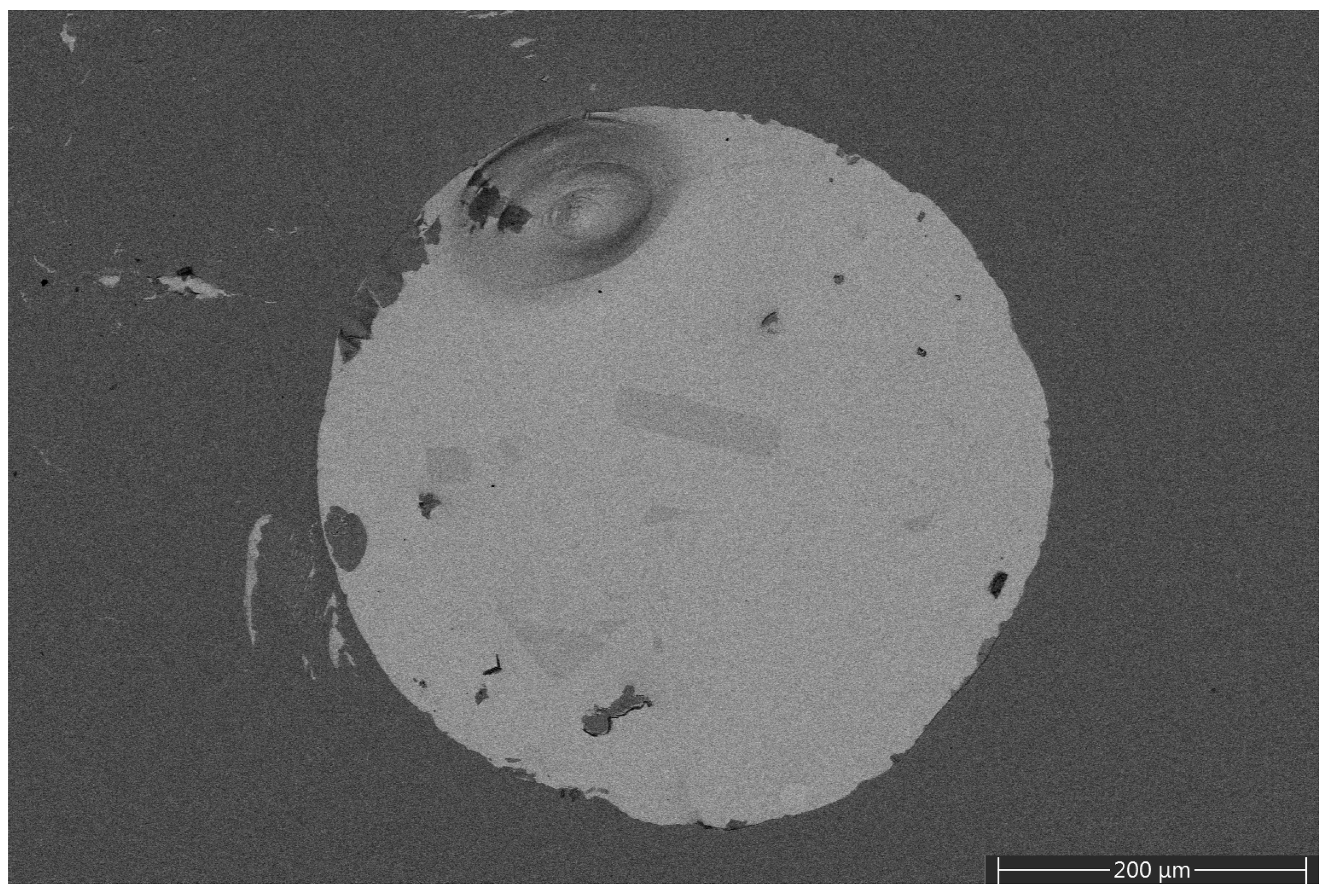
Sputtering using 1400 V DC target potential resulted in the formation of a few metallic-looking droplets on the surface of the samples that were even observable via an optical microscope. A backscattered electron micrograph of such a droplet is shown on
Figure 5. It is evident from the image that the droplet has a higher average atomic number than the surrounding area. This was confirmed via EDS, which proved that the droplet mainly contains gallium, and only a minimal amount of oxygen. Note, however, that these droplets were found only occasionally and, apart from them, the samples show a homogeneous composition on the scale investigated via SEM-EDS (see the backscattered electron image of
Figure S1 of the Supplementary Materials). Furthermore, such surface features could not be observed for the films prepared at 1200 V or 1300 V. Thus, using a lower DC target potential, i.e., a lower sputtering power, offers the benefit of better film quality.
Figure 6a shows the refractive indices (
n) and extinction coefficients (
k) of the reactively sputtered (at 1400 V DC target potential) gallium oxide layers as a function of the wavelength, determined via spectroscopic ellipsometry (for additional information, see
Figure S2 and Table S4 of the Supplementary Materials). In general, the films prepared using an oxygen flow of 9–32 sccm have similar
n and
k values. It is noteworthy that the extinction coefficient becomes zero in the UV range at 300 nm; thus, it has potential for solar-blind applications. The sample deposited at an oxygen flow of 6 sccm (0.035 Pa partial pressure) shows a higher refractive index in most of the studied wavelength range, and its
k value also cuts off at a higher wavelength (400 nm). Similar observations were also made for the films sputtered at a 1300 V DC target potential; however, at 1200 V, only slight differences could be observed between the optical parameters of the different samples (see
Figure S3 of the Supplementary Materials). This behavior can be interpreted in terms of the oxygen content of these layers, if the refractive index (at 632.8 nm) is plotted as a function of the oxygen atomic ratio (see
Figure 6b). A general trend in the value of
n can be observed, namely that the layers with a higher oxygen content, i.e., closer to the Ga
2O
3 stoichiometry, present lower refractive indices. The measured values are comparable to the refractive indices of gallium oxide thin films prepared via other deposition techniques, such as plasma-enhanced atomic layer deposition (
n = 1.78–1.88, depending on the oxygen partial pressure) [
26] and electron-beam evaporation (
n = 1.85) [
27].
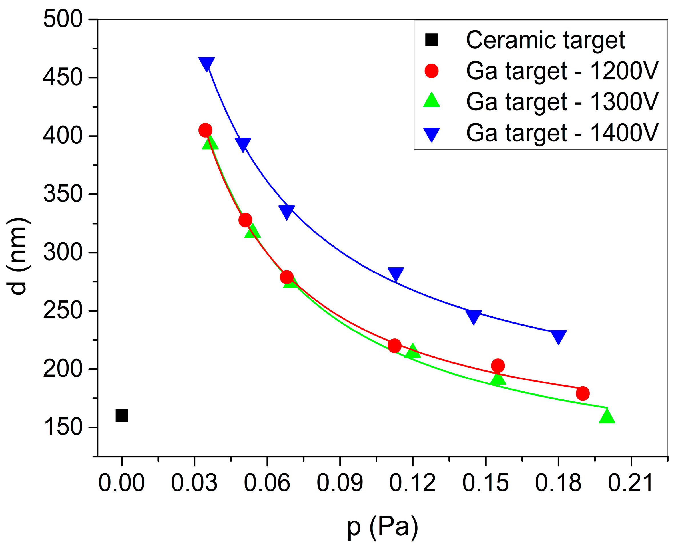
Figure 7 shows the thickness of the deposited films, determined via spectroscopic ellipsometry, at different oxygen partial pressures. Note that, for the 1200 V samples, a 40 min deposition time was used, instead of 30 min. If one compares these thickness data to the thickness of the reference sample sputtered from the ceramic target (d
ref = 160 nm), it is evident that significantly higher deposition rates can be achieved using a liquid Ga target, while maintaining a similar composition. To be specific, using the liquid Ga target and 20 sccm O
2 flow (0.113 Pa O
2 pressure), 9.4 nm/min (for 1400 V), and 5.5 nm/min (for 1200 V) deposition rates were achieved; while using the ceramic target (1400 V), only a 5.3 nm/min deposition rate was measured.
Visual inspection of the target after sputtering shows islands of oxide on its surface (see the whitish areas on top of the target,
Figure 1a,b). An increased oxygen admission results in a higher coverage, as can be seen through comparing
Figure 1a and
Figure 1b. Such a pattern was also observed in an earlier report that demonstrated that oxide forms islands with fractal-like structures on the liquid Ga surface [
28]. It is most probable that such a visually observable oxide layer is more than one monolayer thick. Thus, the assumption of the original Berg model that only a monolayer of the compound exists on the surface does not hold. Hence, the calculations to derive the sputtering yields and sticking coefficient were based on the upgraded Berg model. The solid lines in
Figure 7 show the fit of the thickness data using Equation (4), according to the model presented in
Section 2.3. Here, the reactive gas partial pressure data measured before the sputtering experiment were used, instead of the actual reactive gas pressure, as this could not be measured in our experimental setup during sputtering. The fitted parameters are given in
Table 1. The sputtering yield of Ga (
Ymm) is close to the values estimated using SRIM simulations [
29], i.e., 1.9, 2.04 and 2.15 for 1200 V, 1300 V, and 1400 V, respectively. As expected, the partial sputtering yields are significantly lower than the sputtering yield of pure gallium. Increasing the DC target potential (and, consequently, increasing the sputtering power) results in increased Ga yields; however, the partial sputtering yield of oxygen atoms decreased while their knock-in yield increased. This means that, at higher DC target potentials, due to the more energetic incoming ions, the knock-in implantation mechanism becomes more and more significant, compared to the case of 1200 V. This also leads to an increase of the preferential sputtering in favor of Ga with the increase of the DC target potential. The sticking coefficient shows a decreasing tendency upon the increase in the DC target potential. The value of the sticking coefficient can also be estimated based on the electronegativity difference of the constituting elements, as presented in ref. [
30] for different metal and oxygen systems. Accordingly, the expected value is around 0.03 for the Ga-O system [
30], which is comparable to the result of the fitting based on the upgraded Berg model.
Based on the above findings, the main benefit of the liquid Ga target compared to the ceramic Ga
2O
3 target lies in the higher deposition rate. The ability to control the composition, i.e., the oxygen content, of the deposited film by changing the oxygen flow rate (see
Figure 3) can also be considered an advantage. On the other hand, liquid Ga is more difficult to manipulate, and can only be used in a configuration where the target can be placed at the bottom of the sputtering chamber.


 ,
, 


