Abstract
The chemical composition, structure, and physical properties of aluminum nitride (AlN) films obtained using pulsed DC reactive magnetron sputtering in asymmetric bipolar mode have been studied. X-ray diffraction and electron diffraction confirmed the composition of c–axis textured hexagonal AlN films required for piezoelectric applications. The surface of the films obtained is quite smooth; the arithmetic average roughness does not exceed 2 nm. Transmission electron microscopy has shown the presence of a transition layer at the film–substrate interface. Transmission electron microscopy and X-ray photoelectron spectroscopy depth profile analysis have shown that the films have an oxidized surface layer which has an influence on the optical model of the films derived from ellipsometric data. However, it does not significantly influence the films’ piezoresponse. Piezoelectric force microscopy indicated a piezoelectric effect in the films that is uniform over their surface.
1. Introduction
Aluminum nitride (AlN), along with zinc oxide (ZnO), has been used in microelectromechanical systems since the 1970s due to its high piezoelectric properties. More recently, AlN films have been used in high-frequency applications, in particular in telecommunication technologies at frequencies in the gigahertz range. Currently, piezoelectric AlN films have the widest scope of application in radiofrequency devices compared to other materials [1]. This is facilitated by a number of unique physical properties of AlN films in addition to the piezoelectric effect. High values of thermal conductivity, band gap, hardness, speed of sound, and low signal propagation losses make AlN an attractive material for radio frequency electronics [2].
AlN films are used to create resonators operating on surface acoustic waves (SAW) [3] and bulk acoustic waves (BAW) [4]. At present, technologies for obtaining multilayer thin-film resonators operating on BAW are actively developed and widely used to create frequency-selective devices and generate signals with a frequency from 2 to 20 GHz [5,6,7]. These resonators are multilayer structures containing a piezoelectric transducer and an acoustic Bragg reflector. An essential part of multilayer resonators is the AlN thin film, which works as a piezoelectric transducer [8]. However, the quality and major quantitative characteristics of grown AlN significantly depend on the technology of their fabrication [9].
AlN thin films can be synthesized using various deposition methods, for example, chemical vapor deposition (CVD) [10], plasma enhanced chemical vapor deposition (PECVD) [11], molecular beam epitaxy (MBE) [12], metal-organic chemical vapor deposition (MOCVD) [13], atomic layer deposition (ALD) [14], ion beam sputtering [15], filtered cathodic vacuum arc (FCVA) [16], pulsed laser deposition (PLD) [17], and direct current (DC) or radio-frequency (RF) reactive magnetron sputtering [18,19]. DC reactive magnetron sputtering is the most commonly used method for the deposition of AlN thin films in microelectromechanical technology due to its low cost, simplicity, low temperature requirement, and reproducibility [20,21]. AlN films deposited using this method are polycrystalline, and may have a perfect c-axis orientation and piezoelectric activity [1,22]. Such films have properties comparable to AlN epitaxial films, which can be explained by the hexagonal symmetry of AlN [1]. The growth of crystallites strictly along the c-axis leads to the isotropy of physical properties in the substrate plane, i.e., to the insensitivity of physical properties to the orientation of crystallites in this plane [1].
Pulsed DC magnetron sputtering is a method that has been applied since the 1980s when the problem of dielectric films synthesis appeared. Pulsed DC magnetron discharge can be produced by asymmetric bipolar, symmetric bipolar, or unipolar pulsed waveforms, depending on power supply [23]. The deposition of dielectrics via the method of reactive magnetron sputtering of a metal target in the presence of a reactive gas leads to the formation of non-conductive layers on the target surface, which is called target poisoning. These layers become positively charged under the influence of the magnetron plasma [24]. As a result, the target sputtering rate is reduced, because argon ions can no longer efficiently sputter its surface [23]. Charges on the target surface create arcs that cause its erosion in the form of macroparticles (solid fragments or drops of the target material). These macroparticles degrade the quality of the film, and arcs can even damage the power supply [24]. An asymmetric bipolar pulsed DC discharge eliminates target poisoning. The amplitude of the negative voltage pulse is greater than the amplitude of the positive pulse. The width of the positive voltage pulse is typically 10%–20% of the width of the negative pulse. With a negative pulse, the target is sputtered with argon and reactive gas ions. When the target surface is positively charged, the sputtering efficiency decreases. With a positive pulse, the charge on the target is neutralized by the electron flow that sputters the non-conductive layer [23].
Nevertheless, the practical deposition of structurally perfect AlN thin films uing magnetron sputtering is not an easy task. Firstly, it is difficult to select the deposition process conditions under which the films contain a single hexagonal AlN phase with an ideal crystallite texture in the c-axis direction [1]. Secondly, the high affinity of AlN for oxygen leads to its incorporation into the films, with subsequent deterioration of their crystallinity and piezoelectric characteristics [25,26,27].
The problem of oxygen’s location and inclusion mechanism in AlN films has been considered in previous publications [28,29,30,31], but this question is still important [32,33,34]. Some possible mechanisms of oxygen inclusion in AlN films were proposed earlier. A characteristic decrease in the oxygen concentration from the film surface towards the substrate was observed in most publications regarding film depth profile analysis [28,29,32]. This profile is most likely due to the oxidation of the films as a result of their removal from the vacuum chamber, and further storage of samples in the air, where a hydrolysis reaction can occur in a moist atmosphere [32]. The authors of [30] claimed that oxygen in small concentrations (about 0.75 at. %) incorporates into the crystal lattice of AlN in the form of O2− anions instead of N3− anion vacancies to compensate for the positive charge of Al3+ cations. According to [31], oxygen-containing AlN films have separate AlxOy domains that cause the disordering of the AlN crystal structure. The authors of [33] attribute oxygen inclusion to the magnitude of sputtering voltage, which accelerates the electronegative oxygen (O−) ions toward the film surface. In the authors’ opinion, a high sputtering voltage leads to an increase in the number of implanted and trapped oxygen species, and eventually to the formation of crystallites with crystallographic orientations other than (002) in the AlN films [33]. In [34], films with controlled oxygen content were deposited using RF magnetron sputtering from the AlN target in the N2 flow. It was found that oxygen content increases with an increase in N2 flow, so the authors concluded that the oxygen source originates from trace O2 impurities in N2 gas.
The aim of this work is to study the chemical composition, structure, and physical properties of AlN films deposited on silicon substrates via pulsed DC reactive magnetron sputtering. In addition, an important task of the work is to study the origin and location of oxygen in AlN films. The process conditions were selected to obtain single-phase films with an AlN hexagonal phase only, and a strict crystallite orientation in the (002) plane.
2. Materials and Methods
AlN films were deposited by pulsed DC reactive magnetron sputtering from an aluminum target with a purity of 99.99%. The magnetron (Applied Electronics, Tomsk, Russia) was powered by 1.8 kW APEL-M-1.5BP-800 DC power supply operating in an asymmetric bipolar pulsed DC mode at a frequency of 100 kHz. Before deposition, the vacuum chamber was pumped out to a base pressure of 2 × 10⁻⁴ Pa. The aluminum target was pre-sputtered for 10 min with the shutter closed to clean the surface. The deposition was carried out at a discharge power of 150 W. The sputtering and reactive gases (argon and nitrogen, respectively) were fed into the target zone through a gas distribution ring mounted on top of the magnetron, which improved the spatial homogeneity of the gas mixture. This approach has previously demonstrated effectiveness in studies [35,36]. The purity of the gases was 99.999%. The argon mass flow was 80 sccm, and nitrogen was 20 sccm. The flow rates of gases were regulated by separate mass flow controllers SEC512MG (HORIBA Trading Co., Ltd., Beijing, China). After feeding the working gas mixture, the working pressure in the chamber reached 0.2 Pa. The deposition of AlN films was carried out for 100 min on silicon substrates heated up to 300 °C. Czochralski-grown single crystal boron-doped Si wafers with crystallographic orientation (111), p-type conductivity, and a specific resistance of 0.85–1.15 Ω × cm were used as substrates. The substrate surface was parallel to the target surface, and was located at a distance of 80 mm from it. Three deposition processes were carried out on different days with the same process parameters in order to verify the reproducibility of AlN films.
X-Ray diffraction (XRD) analysis of the samples was performed on an ARL X’TRA diffractometer (Thermo Fisher Scientific, Ecublens, Switzerland) equipped with a Cu–Kα (λ = 1.5418 Å) source. The 2θ range was from 15° to 85° with a step of 0.05° and an exposition of 5 s per a point. Phase analysis was performed using the values of interplanar distances calculated according to the Bragg–Wulff equation:
where d is the interplanar distance, n′ is the order of reflection (i.e., diffraction order).
The reference data were obtained from the PDF-2 database. Calculation of the coherent scattering region (CSR) was carried out using the Scherrer formula considering the instrumental broadening of the peaks (the α–Al2O3 external standard):
where D is the coherent scattering region size, K is the numerical coefficient (taken as 1), β is the full-width at half maximum (for reflection 002).
Scanning electron microscopy (SEM) images and the elemental composition of the AlN films were obtained using a JSM 6700F electron microscope (JEOL, Tokyo, Japan) equipped with a Quantax 200 energy dispersive analyzer (Bruker Nano GmbH, Berlin, Germany). The acceleration voltage of the electron beam was 15 keV during the capturing of images. The energy-dispersive X-Ray spectroscopy (EDS) studies were carried out at an accelerating voltage of the electron beam of 5 keV. This value was chosen because it is insufficient for the beam to reach the silicon substrate. This made it possible to exclude the influence of the substrate on the results of the analysis.
Lattice vibrations in the AlN films were investigated using IR spectroscopy. IR absorption spectra were recorded using a Philips Pye Unicam PU9512 double-beam infrared spectrophotometer (Philips Pye Unicam, Cambridge, UK) in the spectral range of 1200–200 cm−1, with a resolution of 2 cm−1. An uncoated silicon substrate was the reference for 100% transmission.
Ellipsometric measurements were performed on a laser null ellipsometer to evaluate thickness d and refractive index n of the films. Light source is a helium-neon laser (λ = 632.8 nm). The ellipsometric angles ψ and Δ were measured at five light incidence angles from 50° to 70° with a step of 5°. The error in measuring the angles ψ and Δ was 2’. The optical path length dn of the films was evaluated via spectrophotometry using techniques previously described in [37]. The thicknesses and refractive indices of the films were reconstructed from the angular dependences of ψ and Δ by solving the inverse problem of ellipsometry (IPE). The optical constants of silicon were assumed to be n = 3.865, k = 0.023. The solution of the IPE was found by minimizing the objective function mean squared error (MSE):
where N is the number of angles of light incidence on the sample (N = 5); ψie and Δie are the experimental values of the ellipsometric angles at the i–th angle of incidence; ψic and Δic are the values calculated for the given model. IPE was solved using one-layer and two-layer models.
The depth profiles of the atomic concentrations were obtained using an X-ray photoelectron spectrometer (XPS) FlexPS (SPECS Surface Nano Analysis GmbH, Berlin, Germany) equipped with a Phoibos 150 analyzer (SPECS Surface Nano Analysis GmbH., Berlin, Germany) with a 1D–DLD electron detector (SPECS Surface Nano Analysis GmbH., Berlin, Germany). The XPS spectra were recorded using a monochromatic Al Kα (λ = 8.3386 Å) source. Film etching was carried out with a scanning Ar+ ion beam over an etching area of 5 mm × 5 mm. The ion current was 48 μA. The XPS spectra of the films were recorded before etching, 1 min after the etching start and then every 10 min, while the overall etching time was 61 min. Atomic concentrations were calculated from the spectra area after subtracting the background of the inelastically scattered electrons. The photoionization cross section, electron free path, and instrumental function of the spectrometer were also considered for correct determination of the composition. After XPS studies, the cross-section SEM images of the films were obtained at two areas, i.e., at the center of the etching area and outside the etching area.
High-resolution transmission electron microscopy (HRTEM) and high-angle annular dark-field scanning transmission electron microscopy (HAADF-STEM) data were obtained using a JEOL JEM-2200FS electron microscope (JEOL, Tokyo, Japan) with a resolution of 0.23 nm and an accelerating voltage of 200 kV. During the preparation of the sample to study on TEM, two pieces of the sample films were glued to each other with epoxy resin, after which the grinding and etching procedure is carried out. Grinding was carried out on the installation “Leica EM EXP” (Leica Mikrosysteme GmbH., Wien, Austria) in two stages on both sides using diamond grinding discs with different grain sizes (9, 6, 2, 0.5 µm). After completion of the mechanical thinning procedure, a special copper ring 3 mm in diameter was glued onto the sample with epoxy resin. Next, the ion etching was carried out using a Gatan ion etching station “Precision Ion polishing system PIPS model 691” (Gatan Inc., Pleasanton, CA, USA), in a double regime at an accelerating voltage of the electron beam of 5 keV. A copper ring was placed with the sample in the vacuum chamber of the setup, where the sample was thinned for two hours using two argon beams. The ion beams formed the ion guns, which were directed to the sample at an angle of 6° while the sample itself rotated. The microscope was equipped with an energy-dispersive X-Ray (EDX) analyzer with an energy resolution of 133 eV (JEOL, Tokyo, Japan). Interplanar spacings were evaluated using fast Fourier transforms (FFT) of the crystal lattice and using DigitalMicrograph software (Gatan Inc., Pleasanton, CA, USA) (version 1.8).
The surface morphology of the AlN films was investigated via atomic force microscopy (AFM) on a Bruker Dimension Icon scanning probe microscope (Bruker, Santa Barbara, CA, USA) in the tapping mode, using a sharp ScanAsyst-AIR probe (Bruker, Santa Barbara, CA, USA) with a beam cantilever stiffness coefficient of 0.4 N/m, a resonant frequency of 70 kHz, and a nominal radius roundness of 4 nm. A DLgram01 service (NSU, Novosibirsk, Russia) [38] was used to assess statistical data (size and number of crystallites) from the AFM images. The piezoelectric force microscopy (PFM) studies were further performed on the microscope in the piezoresponse mode using a conductive SCM-PIT-V2 probe (Bruker, Santa Barbara, CA, USA) with a beam cantilever stiffness coefficient of 3 N/m, a resonant frequency of 75 kHz, and a nominal radius roundness of 25 nm, coated with platinum–iridium (PtIr) alloy for electrical measurements. All data acquired by AFM were processed in the NanoScopeAnalysis 1.50 software (Bruker, Santa Barbara, CA, USA).
3. Results and Discussion
The phase composition, structure, and coherent scattering region (CSR) size of AlN films have been determined via X-ray diffraction. The diffraction patterns of the samples (Figure 1) show the narrow 002 and 004 reflections of the hexagonal AlN with interplanar distances of 2.497 and 1.244 Å according to the Bragg equation. The additional low intensity reflection belongs to the silicon wafer. The existence of these reflections as much as the absence of other AlN reflections, such as 101 or 103, allow us to confirm that the deposited AlN has a c-axis texture close to that of epitaxial films. CSR values calculated using the Scherrer formula were in the range of 60–65 nm for all samples, which evidences their highly crystallized structure. Thus, X-ray diffraction analysis exhibits the phase composition and texture of AlN films that are mostly favorable for piezoelectric applications [1].
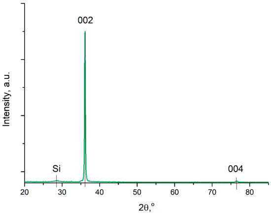
Figure 1.
X-ray diffraction patterns of AlN/Si(111) sample.
The SEM images (Supplementary Materials, Figure S1) do not contain any pronounced features of the surface morphology, which indicates the smoothness of the film surface, further verified by AFM. According to the elemental composition data (a typical EDS spectrum is in Supplementary Materials, Figure S2), the films contain 42–43 at. % of aluminum, 47–48 at. % of nitrogen, 6–7 at. % of oxygen, 0–3 at. % of carbon, and 0–2 at. % of argon. Carbon appeared in the analysis results spontaneously. With several analyses of the same sample at different times and at different points on the surface, the carbon concentration differs, so we attribute the carbon to surface contamination. Argon also appeared spontaneously. We believe that its origin in the films is associated with the capture of argon atoms by the growing film so that it cannot escape from it. Argon in the films deposited by magnetron sputtering was also observed in other works [39]. It should be noted that the obtained atomic concentrations are integrated values related to the thickness through which an electron beam with an energy of 5 keV can penetrate. Our calculation using Casino 2.42 software (Universite de Sherbrook, Quebec, QC, Canada) [40] showed that the penetration depth of an electron beam with energy of 5 keV into AlN (that is, the depth of analysis) is no more than 350 nm, which is three times less than the film thickness.
The IR absorption spectra of AlN films were recorded in the range of 1200–200 cm−1; a band is observed with a maximum at about 675 cm−1 (Figure 2), which is related to E1(TO) phonon band of hexagonal AlN [25,41,42,43]. The predominance of this band indicates the preferential orientation of the film crystallites in the c-axis direction [43], which is in agreement with XRD results. The feature at 1106 cm−1 is a consequence of the incomplete compensation of the spectrum on an uncoated substrate, and corresponds to interstitial oxygen, which always presents in silicon [44]. In the low-frequency region of the spectrum (300–200 cm−1), weak rotational bands of atmospheric water are observed, since the spectrometer cuvette was not purged with dry gas during the studies.
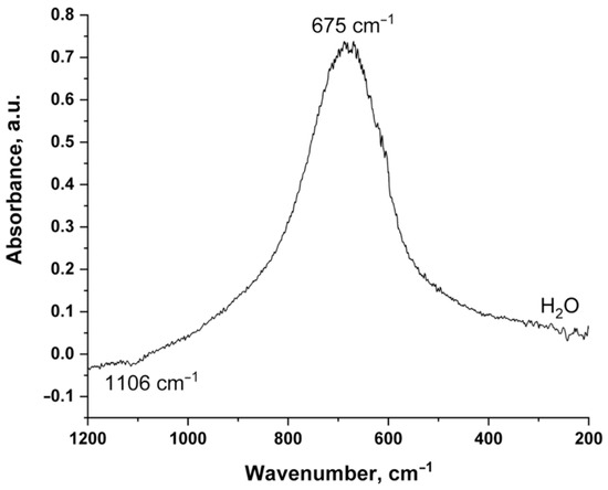
Figure 2.
Typical IR spectrum of AlN/Si(111) samples.
When solving the IPE, the single-layer and two-layer models of the films were successively used to describe the optical properties of the samples. The calculated parameters for the one-layer model were used as an initial approximation to construct the two-layer model. The results of IPE solutions are shown in Figure 3 as diagrams illustrating the position of the substrate and all layers of the model, and MSE values as well. For the single-layer model of a film, the MSE value significantly exceeds the measurement error of ψ and Δ. This means that the one-layer model incorrectly describes the structure of a real sample. The two-layer model fits much better. According to this model, the upper layer has a refractive index close to that of Al2O3, and the lower layer has a refractive index close to that of polycrystalline AlN [45]. The presented results of mathematical modeling do not mean that the refractive index profile calculated using the two-layer model corresponds to the true profile of the sample. We can only assume that the AlN films have a surface layer with a reduced refractive index. It is known that refractive index of AlN films has a complex thickness profile with a characteristic decrease in the oxygen concentration from the film surface towards the substrate [28,29,32]. We assume our samples have a similar structure.
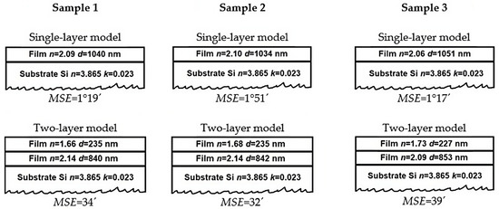
Figure 3.
The results of solving the IPE for AlN/Si(111) samples, presented as diagrams of the “film–substrate” system.
A depth profile analysis of the AlN film was carried out using the XPS method with in situ ion etching for 61 min. The composition of the AlN film was almost constant (Table 1) after 21 min of etching. We can see that there are impurities on the surface of the films. The carbon concentration is very small, while the oxygen concentration is markable after 21 min of etching (see also Supplementary Materials, Figures S3 and S4). Argon appears in the films as a result of argon ions’ penetration from an ion source, but a comparable concentration of argon is sometimes detected via EDS in the deposited AlN films. Notably, the EDS results in the center of the etching area were almost the same as EDS results in the non-etched area of the film. However, the nitrogen concentration determined using XPS after etching is significantly lower than that determined using EDS. So, we conclude that nitrogen atoms are preferably (selectively) emitted from the film during etching. A similar result was reported in [45].

Table 1.
Chemical composition of the AlN/Si(111) sample before ion etching and after 21 min ion etching based on XPS compared to SEM EDS.
The oxygen depth profile of XPS (Figure 4) is evidence of a gradient oxidized surface layer similar to that presented in [28,29,32]. It was found from an SEM cross-sectional view that the initial film thickness was 1040 nm, which is in excellent agreement with the results of ellipsometry (1030–1050 nm), and the film thickness in the etched area appeared to be 850–870 nm (Figure 5). So, the layer of 170–190 nm was sputtered from the AlN film during etching with a rate of 2.8–3.2 nm/min. Stabilization of the chemical composition was reached at a depth of about 60 nm from the film surface. This verifies the suggestion that a high MSE value is a consequence of an inadequate one-layer optical model that cannot correctly describe the gradient surface layer. In addition, the optical properties can be affected not only by the chemical composition, but also by the structural features of the film [46]. This issue requires further study.
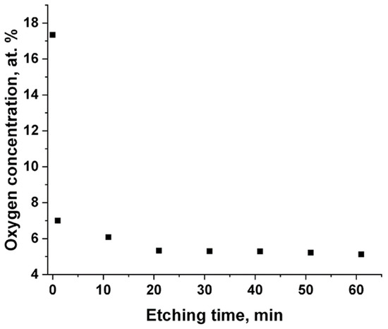
Figure 4.
Oxygen depth profile of the AlN/Si(111) sample on the basis of XPS.
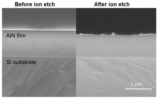
Figure 5.
SEM cross-sectional view of AlN/Si(111) sample before and after ion etching in the XPS chamber. Film–substrate interfaces are intentionally matched for clarity.
The images of the microstructure and crystal orientation of the AlN film were also obtained via HRTEM (Figure 6). AlN crystallites are oriented in the (002) plane perpendicular to the substrate surface, as expected. Additionally, the thin transition layer was found at the film–substrate interface. The sample thickness varies from 900–1000 nm, and this non-significant variation is due to the features of the sample preparation process.
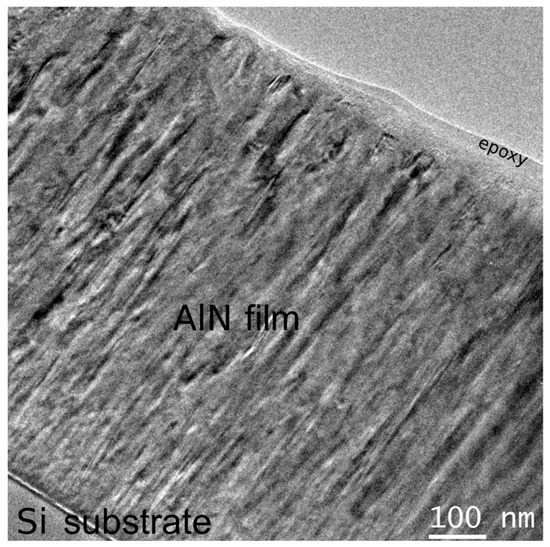
Figure 6.
Typical TEM image of the crystal structure of AlN/Si(111).
An estimate of interplanar distances was obtained using the Fourier transform (FFT) of the crystal lattice from the HRTEM images (Figure 7a). The value of interplanar distance obtained by fast Fourier transformation (FFT) of the crystal lattice image (Figure 7a) is approximately 2.5 Å, and correlates with the interplanar distance from the XRD patterns. The transition layer between the substrate and the AlN film is presented on HRTEM image (Figure 7b), and is possibly formed at the initial stage of the film growth. Use of a buffer layer for better AlN or GaN growth has previously been described, for example, in [47,48]. The thickness of the transition layer is approximately 20 nm, and it perhaps plays the role of the substrate for desirable columnar growth. Figure 8 shows the composition maps obtained during the EDX analysis in the HAADF-STEM mode. The transition layer between the substrate and the film is visible in the HAADF-STEM mode (Figure 8a). From the analysis of elemental maps from TEM, we suggest that transition layer consisted of amorphous AlN with possible inclusions of silicon. The increased oxygen content in the near-surface layer of a thin film is apparently associated with oxidation processes. The distribution of the aluminum in the film is quite uniform.
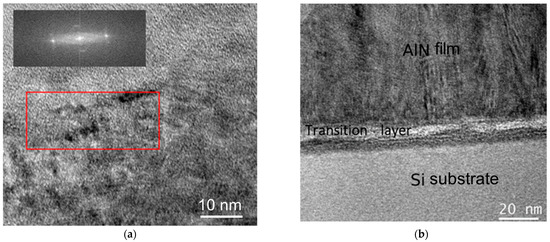
Figure 7.
Exemplary HRTEM-images of an AlN/Si sample: (a) the crystal lattice in the middle of AlN film and FFT from the area selected as a red rectangle; and (b) the transition layer between the substrate and polycrystalline AlN film.
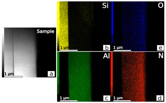
Figure 8.
EDX maps of elements: (a) sample image in HAADF-STEM mode, (b) silicon, (c) aluminum, (d) nitrogen, (e) oxygen.
Processing of the AFM images of the AlN films (Figure 9) gives an arithmetic mean roughness value of Sa = 1.6 nm. Low roughness is required for piezoelectric applications [1]. The DLgram01 service allowed automatic image processing by training a neural network prior to obtaining detailed information about all the recognized objects. The image of the AlN film surface after processing allowed us to highlight the shapes and sizes of surface morphological features (Figure 10a) and a particle (i.e., round-shaped objects) size distribution histogram (Figure 10b). The average particle size over the entire sample is 58 nm, with a standard deviation of 18 nm. This value correlates well with the aforementioned value of CSR from XRD, although one needs to consider that objects observed by AFM are not an ideal round shape. A typical enlargement of the size of all objects visualized via AFM took place due to the convolution of the shapes of the sample and the AFM tip.
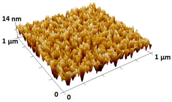
Figure 9.
Typical 3D-AFM image of the AlN/Si(111) samples for 1 μm × 1 μm area. The vertical Z-scale (14 nm) is enlarged to highlight the roughness features.
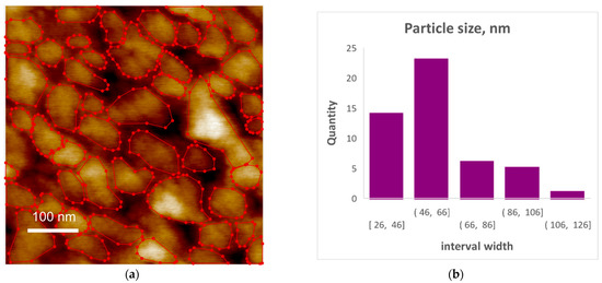
Figure 10.
Results of the DLgram01 service modelling: (a) recognized surface morphological features of the DLgram01 service, and (b) particle size distribution histogram.
The piezoelectric effect has been found to be uniform all over the scanned surface region (5 µm × 5 µm) without any apparent domains. A piezoelectric coefficient d33 of the AlN films was roughly estimated using a LiNbO3 single-crystal reference; a value of 4 ± 1 pm/V was obtained. According to the literature data [9], a d33 close to 4 pm/V is common for polycrystalline AlN thin films. Considering this, it may be concluded that the AlN films produced by pulsed DC reactive magnetron sputtering provide quite high piezoelectric properties.
4. Conclusions
The growth of AlN films was performed by pulsed DC reactive magnetron sputtering in an asymmetric bipolar pulsed DC mode. The surface of the films turned out to be nanosmooth (i.e., having a roughness of <2 nm, according to the AFM data). The high orientation of the crystallites in the [002] direction was proved using XRD and IR spectroscopy, and the refractive index of the films corresponds to the published values for AlN. Visualization of atomic packing under an electron microscope proved the high ordering and low defectiveness of hexagonal AlN crystals. A transition layer with a thickness of about 20 nm has been found at the substrate–film interface using HRTEM, and this may be the initial layer for c-axis growth. An XPS depth profile analysis, EDX analysis in the HAADF-STEM mode, and ellipsometry confirm the presence of an oxidized surface layer. It is remarkable and unexpected that deviation from the ideal AlN stoichiometry and the impurities do not worsen the quality of the AlN films. The key application characteristic for AlN films is the value of the piezoelectric coefficient. This was measured using PFM, and a value of 4 pm/V was determined, which corresponds to the values for polycrystalline AlN, it being less than the typical 5 pm/V for a single-crystal AlN. We selected AlN film growth parameters that allowed us to deposit hexagonal AlN films with high smoothness, appropriate chemical composition, and c-axis texture in a fast and repeatable way; these are highlighted in the manuscript and can be considered optimal. The obtained results contribute to the development of film SAW-/BAW-micro resonator technology, and can be implemented by other researchers and manufacturers for growing AlN films.
Supplementary Materials
The following supporting information can be downloaded at: https://www.mdpi.com/article/10.3390/coatings13071281/s1, Figure S1: Typical SEM images of AlN/Si(111) samples at 50 k (a) and 200k (b) magnification; Figure S2: A typical EDS spectrum of AlN film; Figure S3: C1s XPS spectra AlN films measured before ion etching (a) and after 11 min etching (b); Figure S4: Al2p XPS spectra of AlN films measured before ion etching (a) and after 11 min etching (b).
Author Contributions
Conceptualization, V.R.S.; Formal analysis, I.P.A. and E.A.M.; Funding acquisition, P.V.G.; Investigation, V.R.S., A.L.B., S.Y.C., I.P.A., E.A.M., A.V.K., M.I.M. and A.V.L.; Methodology, S.Y.C.; Supervision, P.V.G.; Writing—original draft, V.R.S., A.L.B., S.Y.C., A.V.K. and P.V.G.; Writing—review and editing, A.L.B. All authors have read and agreed to the published version of the manuscript.
Funding
This research was funded by the Ministry of Education and Science of Russia, grant No. FSUS-2020-0029.
Institutional Review Board Statement
Not applicable.
Informed Consent Statement
Not applicable.
Data Availability Statement
The data presented in this study are available on request from the corresponding authors.
Acknowledgments
The authors acknowledge the Shared Research Center “VTAN” of the Novosibirsk State University, supported by Minobrnauki of Russia, under agreement #075-12-2021-697. The authors are thankful to A. O. Geydt for assistance with manuscript translation, V. A. Volodin for valuable discussions on optical measurements, and acknowledge the late A. S. Zolkin for their invaluable efforts in building the dielectric film growth setup.
Conflicts of Interest
The authors declare no conflict of interest. The funders had no role in the design of the study; in the collection, analyses, or interpretation of data; in the writing of the manuscript; or in the decision to publish the results.
References
- Muralt, P. AlN Thin Film Processing and Basic Properties. In Piezoelectric MEMS Resonators; Bhugra, H., Piazza, G., Eds.; Springer Nature: Berlin, Germany, 2017; pp. 3–37. [Google Scholar]
- Assylbekova, M.; Chen, G.; Pirro, M.; Michetti, G.; Rinaldi, M. Aluminum nitride combined overtone resonator for millimeter wave 5G applications. In Proceedings of the 2021 IEEE 34th International Conference on Micro Electro Mechanical Systems (MEMS), Virtual Conference, 25–29 January 2021; pp. 202–205. [Google Scholar]
- Zhou, J.; Pang, H.F.; Garcia-Gancedo, L.; Iborra, E.; Clement, M.; De Miguel-Ramos, M.; Jin, H.; Luo, J.K.; Smith, S.; Dong, S.R.; et al. Discrete microfluidics based on aluminum nitride surface acoustic wave devices. Microfluid. Nanofluidics 2015, 18, 537–548. [Google Scholar] [CrossRef]
- Li, C.; Liu, X.; Shu, L.; Li, Y. AlN–based surface acoustic wave resonators for temperature sensing applications. Mater. Express. 2015, 5, 367–370. [Google Scholar] [CrossRef]
- Torgash, T.N.; Kozlov, A.G. Influence of Spacer in Acoustic Reflector on Parameters of Microelectronic BAW Resonators. In Proceedings of the 2020 Wave Electronics and its Application in Information and Telecommunication Systems (WECONF), Petersburg, Russia, 3–7 June 2020; pp. 1–4. [Google Scholar]
- Sorokin, B.P.; Novoselov, A.S.; Kvashnin, G.M.; Luparev, N.V.; Asafiev, N.O.; Shipilova, A.B.; Aksyonenkov, V.V. Development and Study of Composite Acoustic Resonators with Al/(Al, Sc)N/Mo/Diamond Structure with a High Q Factor in the UHF Range. Acoust. Phys. 2019, 65, 263–268. [Google Scholar] [CrossRef]
- Baranova, L.V.; Strunin, V.I.; Chirikov, N.A. Influence of magnetron sputtering modes of aluminum and aluminum nitride films on their surface, structure and composition. J. Phys. Conf. Ser. 2020, 1870, 012023. [Google Scholar] [CrossRef]
- Felmetsger, V.V. Sputter technique for deposition of AlN ScAlN and Bragg reflector thin film in mass production. In Proceedings of the 2017 IEEE International Ultrasonics Symposium (IUS), Washington, DC, USA, 6–9 September 2017; pp. 1–5. [Google Scholar]
- Fei, C.; Liu, X.; Zhu, B.; Li, D.; Yang, X.; Yang, Y.; Zhou, Q. AlN piezoelectric thin films for energy harvesting and acoustic devices. Nano Energy 2018, 51, 146–161. [Google Scholar] [CrossRef]
- Dollet, A.; Casaux, Y.; Chaix, G.; Dupuy, C. Chemical vapour deposition of polycrystalline AlN films from AlCl3–NH3 mixtures.: Analysis and modelling of transport phenomena. Thin Solid Film. 2002, 406, 118–131. [Google Scholar] [CrossRef]
- Sánchez, G.; Wu, A.; Tristant, P.; Tixier, C.; Soulestin, B.; Desmaison, J.; Bologna Alles, A. Polycrystalline AlN films with preferential orientation by plasma enhanced chemical vapor deposition. Thin Solid Film. 2008, 516, 4868–4875. [Google Scholar] [CrossRef]
- Matta, S.; Brault, J.; Korytov, M.; Vuong, P.; Chaix, C.; Al Khalifioui, M.; Vennegues, P.; Massies, J.; Gil, B. Properties of AlN layers grown on c–sapphire substrate using ammonia assisted MBE. J. Cryst. Growth 2018, 499, 40–46. [Google Scholar] [CrossRef]
- Yin, J.; Chen, D.; Yang, H.; Liu, Y.; Talwar, D.N.; He, T.; Ferguson, I.T.; He, K.; Wan, L.; Feng, Z.C. Comparative spectroscopic studies of MOCVD grown AlN films on Al2O3 and 6H–SiC. J. Alloys Compd. 2020, 857, 157487. [Google Scholar] [CrossRef]
- Li, W.; Xue, W. Structural characterization of AlN thin films grown on sapphire by atomic layer deposition. Thin Solid Film. 2023, 773, 139826. [Google Scholar] [CrossRef]
- Sharma, N.; Ilango, S.; Dash, S.; Tyagi, A.K. X-ray photoelectron spectroscopy studies on AlN thin films grown by ion beam sputtering in reactive assistance of N+/N2+ ions: Substrate temperature induced compositional variations. Thin Solid Film. 2017, 636, 626–633. [Google Scholar] [CrossRef]
- Xie, W.; Zhao, Y.; Chen, S.; Liao, B.; Zhang, S.; Hua, Q.; He, G. Corrosion resistance of AlN monolayer and Al/AlN multilayer deposited by filtered cathodic vacuum arc. Thin Solid Film. 2023, 772, 139762. [Google Scholar] [CrossRef]
- Duta, L.; Stan, G.E.; Stroescu, H.; Gartner, M.; Anastasescu, M.; Fogarassy, Z.; Mihailescu, N.; Szekeres, A.; Bakalova, S.; Mihailescu, I.N. Multi-stage pulsed laser deposition of aluminum nitride at different temperatures. Appl. Surf. Sci. 2016, 374, 143–150. [Google Scholar] [CrossRef]
- Ababneh, A.; Albataineh, Z.; Dagamseh, A.M.K.; Al-kofahi, I.S.; Schäfer, B.; Zengerle, T.; Bauer, K.; Seidel, H. Optical characterization of sputtered aluminum nitride thin films—Correlating refractive index with degree of c-axis orientation. Thin Solid Film. 2020, 693, 137701. [Google Scholar] [CrossRef]
- Sharma, V.; Walia, A.; Kumar, M.; Shukla, V.N. Solid particle erosion of aluminium nitride thin film deposited by radio frequency magnetron sputtering technique on AA6061. Mater. Today Proc. 2021, 46, 6673–6677. [Google Scholar] [CrossRef]
- Iqbal, A.; Faisal, M.Y. Reactive Sputtering of Aluminum Nitride (002) Thin Films for Piezoelectric Applications: A Review. Sensors 2018, 18, 1797. [Google Scholar] [CrossRef]
- Fu, Y.Q.; Luo, J.K.; Nguyen, N.T.; Walton, A.J.; Flewitt, A.J.; Zu, X.T.; Li, Y.; McHale, G.; Matthews, A.; Iborra, E.; et al. Advances in piezoelectric thin films for acoustic biosensors, acoustofluidics and lab-on-chip applications. Prog. Mater. Sci. 2017, 89, 31–91. [Google Scholar] [CrossRef]
- Dubois, M.A.; Muralt, P. Stress and piezoelectric properties of aluminum nitride thin films deposited onto metal electrodes by pulsed direct current reactive sputtering. J. Appl. Phys. 2001, 89, 6389–6395. [Google Scholar] [CrossRef]
- Gudmundsson, J.T. Physics and technology of magnetron sputtering discharges. Plasma Sources Sci. Technol. 2020, 29, 113001. [Google Scholar] [CrossRef]
- Belkind, A.; Freilich, A.; Lopez, J.; Zhao, Z.; Zhu, W.; Becker, K. Characterization of pulsed DC magnetron sputtering plasmas. New J. Phys. 2005, 7, 90. [Google Scholar] [CrossRef]
- Molleja, J.G.; Gomez, B.J.; Ferron, J.; Gautron, E.; Burgi, J.; Abdallah, B.; Djouadi, M.A.; Feugeas, J.; Jouan, P.-Y. AlN thin films deposited by DC reactive magnetron sputtering: Effect of oxygen on film growth. EPJ Appl. Phys. 2013, 64, 20302. [Google Scholar] [CrossRef]
- Vergara, L.; Clement, M.; Iborra, E.; Sanz-Hervas, A.; Garcıa Lopez, J.; Morill, Y.; Sangrador, J.; Respaldiza, M.A. Influence of oxygen and argon on the crystal quality and piezoelectric response of AlN sputtered thin films. Diamond Rel. Mater. 2004, 13, 839–842. [Google Scholar] [CrossRef]
- Akiyama, M.; Kamohara, T.; Kano, K.; Teshigahara, A.; Kawahara, N. Influence of oxygen concentration in sputtering gas on piezoelectric response of aluminum nitride thin films. Appl. Phys. Lett. 2008, 93, 021903. [Google Scholar] [CrossRef]
- Taylor, M.B.; Partridge, J.G.; McCulloch, D.G.; Bilek, M.M.M.; McKenzie, D.R. The influence of deposition rate on the stress and microstructure of AlN films deposited from a filtered cathodic vacuum arc. Thin Solid Film. 2011, 519, 3573–3577. [Google Scholar] [CrossRef]
- Penza, M.; De Riccardis, M.F.; Mirenghi, L.; Tagliente, M.A.; Verona, E. Low temperature growth of rf reactively planar magnetron–sputtered AlN films. Thin Solid Film. 1995, 259, 154–162. [Google Scholar] [CrossRef]
- Harris, J.H.; Youngman, R.A.; Teller, R.G. On the nature of the oxygen–related defect in aluminum nitride. J. Mater. Res. 1990, 5, 1763–1773. [Google Scholar] [CrossRef]
- García–Méndez, M.; Morales–Rodríguez, S.; Shaji, S.; Krishnan, B.; Bartolo–Pérez, P. Structural properties of AlN films with oxygen content deposited by reactive magnetron sputtering: XRD and XPS characterization. Surf. Rev. Lett. 2011, 18, 23–31. [Google Scholar] [CrossRef]
- Fang, L.; Jiang, Y.; Zhu, S.; Ding, J.; Zhang, D.; Yin, A.; Chen, P. Substrate Temperature Dependent Properties of Sputtered AlN:Er Thin Film for In–Situ Luminescence Sensing of Al/AlN Multilayer Coating Health. Materials 2018, 11, 2196. [Google Scholar] [CrossRef] [PubMed]
- Nomoto, J.; Tsuchiya, T.; Yamamoto, T. Well-defined (0001)-oriented aluminum nitride polycrystalline films on amorphous glass substrates deposited by ion plating with direct-current arc discharge. Appl. Surf. Sci. 2019, 478, 998–1003. [Google Scholar] [CrossRef]
- Anjum, F.; Fryauf, D.M.; Gold, J.; Ahmad, R.; Cormia, R.D.; Kobayashi, N.P. Study of optical and structural properties of sputtered aluminum nitride films with controlled oxygen content to fabricate Distributed Bragg Reflectors for ultraviolet A. Opt. Mater. 2019, 98, 109405. [Google Scholar] [CrossRef]
- Golosov, D.A.; Eungsun, B.; Zavadski, S.M. Joint functioning of a magnetron sputtering system and an end-hall ion source. Tech. Phys. 2014, 59, 1326–1333. [Google Scholar] [CrossRef]
- Kubart, T.; Aijaz, A. Evolution of sputtering target surface composition in reactive high power impulse magnetron sputtering. J. Appl. Phys. 2017, 17, 171903. [Google Scholar] [CrossRef]
- Ayupov, B.M.; Zarubin, A.; Labusov, V.A.; Sulyaeva, V.S.; Shayapov, V.R. Search for an Initial Approximation in Solving Inverse Problems in Ellipsometry and Spectrophotometry. J. Opt. Technol. 2011, 78, 350–354. [Google Scholar] [CrossRef]
- Okunev, A.G.; Mashukov, M.Y.; Nartova, A.V.; Matveev, A.V. Nanoparticle Recognition on Scanning Probe Microscopy Images Using Computer Vision and Deep Learning. Nanomaterials 2020, 10, 1285. [Google Scholar] [CrossRef]
- Lee, W.W.Y.; Oblas, D. Argon entrapment in metal films by de triode sputtering. J. Appl. Phys. 1975, 46, 1728–1732. [Google Scholar] [CrossRef]
- Drouin, D.; Couture, A.R.; Joly, D.; Tastet, X.; Aimez, V.; Gauvin, R. CASINO V2.42—A Fast and Easy–to–use Modeling Tool for Scanning Electron Microscopy and Microanalysis User. Scanning 2007, 29, 92–101. [Google Scholar] [CrossRef]
- Prokofyeva, T.; Seon, M.; Vanbuskirk, J.; Holtz, M.; Nikishin, S.A.; Faleev, N.N.; Temkin, H.; Zollner, S. Vibrational properties of AlN grown on (111)–oriented silicon. Phys. Rev. B 2001, 63, 125313. [Google Scholar] [CrossRef]
- Hobert, H.; Dunken, H.H.; Meinschien, J.; Stafast, H. Infrared and Raman spectroscopic investigation of thin films of AlN and SiC on Si substrates. Vib. Spectrosc. 1999, 19, 205–211. [Google Scholar] [CrossRef]
- Sanz–Hervás, A.; Iborra, E.; Clement, M.; Sangrador, J.; Aguilar, M. Influence of crystal properties on the absorption IR spectra of polycrystalline AlN thin films. Diam. Relat. Mater. 2003, 12, 1186–1189. [Google Scholar] [CrossRef]
- Stavola, M. Infrared spectrum of interstitial oxygen in silicon. Appl. Phys. Lett. 1984, 44, 514–516. [Google Scholar] [CrossRef]
- Motamedi, P.; Cadien, K. XPS analysis of AlN thin films deposited by plasma enhanced atomic layer deposition. Appl. Surf. Sci. 2014, 315, 104–109. [Google Scholar] [CrossRef]
- Ababneh, A.; Dagamseh, A.M.K.; Albataineh, Z.; Tantawi, M.; Al-Bataineh, Q.M.; Telfah, M.; Zengerle, T.; Seidel, H. Optical and structural properties of aluminium nitride thin-films synthesized by DC-magnetron sputtering technique at different sputtering pressures. Microsyst. Technol. 2021, 27, 3149–3159. [Google Scholar] [CrossRef]
- Zhang, X.-Y.; Peng, D.-C.; Han, J.; Ren, F.-B.; Jiang, S.-C.; Tseng, M.-C.; Ruan, Y.-J.; Zuo, J.; Wu, W.-Y.; Wuu, D.-S.; et al. Effect of substrate temperature on properties of AlN buffer layer grown by remote plasma ALD. Surf. Interfaces 2023, 36, 102589. [Google Scholar] [CrossRef]
- Riah, B.; Camus, J.; Ayad, A.; Rammal, M.; Zernadji, R.; Rouag, N.; Djouadi, M.A. Hetero-Epitaxial Growth of AlN Deposited by DC Magnetron Sputtering on Si(111) Using a AlN Buffer Layer. Coatings 2021, 11, 1063. [Google Scholar] [CrossRef]
Disclaimer/Publisher’s Note: The statements, opinions and data contained in all publications are solely those of the individual author(s) and contributor(s) and not of MDPI and/or the editor(s). MDPI and/or the editor(s) disclaim responsibility for any injury to people or property resulting from any ideas, methods, instructions or products referred to in the content. |
© 2023 by the authors. Licensee MDPI, Basel, Switzerland. This article is an open access article distributed under the terms and conditions of the Creative Commons Attribution (CC BY) license (https://creativecommons.org/licenses/by/4.0/).