1. Introduction
Improving the photoelectric conversion efficiency for solar cells has been a hot research topic, especially for space solar cells. It is one of the important methods to prepare thin films or special optical structures on the surface of solar cells, to enhance the absorption of photons by the cells and to improve the photoelectric conversion efficiency, such as various forms of anti-reflection film [
1,
2,
3], suede light-trapping structures [
4,
5], porous structures [
6,
7,
8], etc. The transmittance spectrum of a single-layer anti-reflection film is generally an inverted U-shape, that is, there is a peak transmittance, and the anti-reflection effect is only obvious within a small certain wavelength range. Compared with a single-layer anti-reflection film, a composite multilayer film with a stepwise change in the refractive index can obtain a multi-peak transmittance spectrum, which can broaden the spectral range of high transmittance to a certain extent. However, multilayer films not only need very complex preparation process but also have some thorny problems, such as the interlayer diffusion, interlayer adhesion, interlayer thermal expansion coefficient matching, etc. [
9].
The equivalent refractive index of a porous film can be adjusted by its porosity [
6]. Theoretically, the refractive index of the porous film can be continuously changed, so even a material at a special refractive index that does not exist in nature can be designed. However, the design of porosity is mostly in accordance with statistical laws, and it is nearly impossible to accurately control the structural parameters of the anti-reflection film. More importantly, the high porosity is obviously not conducive to the radiation resistance of the film.
The anti-reflection phenomenon of the surface nanostructure has attracted the attention of a few researchers. Walheim [
10] first proposed to change the equivalent refractive index of an anti-reflection film with a nanostructure to improve its anti-reflection effect. Nayfeh et al. [
11] coated Si nanoparticles on the surface of photovoltaic devices to form a nanostructured film, thereby improving the absorption of ultraviolet and visible light and the photoelectric conversion efficiency of the device. The suede light trapping structure is a representative surface nanostructure. Yuan et al. [
12] coated a sol with polyacrylate/polysilsesquioxane core-shell nanocomposite particles on glass, then calcined it at 500 °C, and prepared super-hydrophilic anti-fogging anti-reflective coating with worm-like nanostructures. Zhao et al. [
5] combined the copper–silver co-catalytic etching method with an alkaline post-treatment process to prepare a submicron suede structure with an average reflectivity of 9.10% in the wavelength range of 300–1000 nm.
In recent years, microprocessing technology has made significant progress. Nanostructures can be prepared with laser etching, physical vapor deposition, chemical vapor deposition, electrochemical deposition, ALD, etc. Sahouane et al. [
13] used chemical vapor deposition technology to plate four-layer and six-layer anti-reflection film made of or on Si material, respectively, and the average reflectance within 300–1100 nm was reduced to 3.26% and 1.05%, respectively. Fu et al. [
14] simulated and designed a new moth-eye structure of Si material and fabricated it by laser interference lithography and inductively coupled plasma etching. In the near-infrared and mid-infrared bands, the average reflectivity in the range of 0–60° is less than 3.5%. Kim et al. [
15] used a layer-by-layer self-assembly method to prepare a transparent super hydrophobic material, in which SiO
2 particles with different sizes were introduced into the multilayer film to adjust the surface roughness and improve the anti-reflection and surface hydrophobic effects.
Nanostructured gratings can have more excellent characteristics for anti-reflection. Firstly, gratings with different periods, duty cycles, and depths can be equivalent to media with different surface roughness, refractive indexes, film thickness, and other parameters. The changing of the grating structure parameters can simulate the desired refractive index materials, even materials that do not exist in nature [
16]. Secondly, the sub-wavelength nano–microstructured grating can be directly etched into the surface of the substrate material, obtaining hydrophobicity and self-cleaning without the design and preparation of anti-reflection film [
17]. Thirdly, nanostructured gratings can achieve wide-band, large-angle, polarization-insensitive anti-reflection [
18,
19,
20]. Based on the above advantages, the subwavelength grating structure has attracted the special attention of researchers. Nanoimprint technology has high resolution and consistency, and the template can be repeatedly used, which greatly reduces the processing cost and effectively reduces the processing time. Therefore, nanoimprint technology is suitable for the preparation of nanostructured gratings. Kanamori et al. [
21] used an aluminum oxide template to prepare an anti-reflection film with a periodic array structure on a silicon substrate with imprinting. In the 400–800 nm wavelength region, the reflection of the silicon surface reduced to 1.6%. Navarro et al. [
22] deposited TiO
2 particles on the film and then used nanoimprint technology to form an array structure, reducing the reflection loss to 0.6% and achieving the dual functions of anti-reflection and self-cleaning.
These research works reported in the literature rarely involved the systematic research and precise control of nanometer anti-reflection structure parameters, such as the period, depth, duty cycle, etc., to meet the demand for the high transmittance of the glass cover for a specific spectrum. Herein, firstly, calculation and simulation were used to investigate the influence of the grating parameters on the light transmittance within the 350–1100 nm wavelength range of the glass cover and the high-energy part of the solar spectrum on Mars and to optimize the parameters of the three-dimensional nanoarray structure. Secondly, nanoimprint and plasma etching were used to prepare nanoarray structures on the surface of the glass covers, of which the parameters were then adjusted by ALD to verify the calculation and simulation results.
Section 2 of the paper introduces the theoretical model of the nanostructures in this study.
Section 3 introduces the experimental methods and processes.
Section 4 calculates the transmittance of glass covers with different grating parameters and discusses the influence of grating parameters on the transmittance. In
Section 5, a nano–microarray structure is constructed on the surface of the glass cover, and the influence of the structural parameters on the transmittance of the cover is discussed.
2. Theoretical Model
When the characteristic size of the nanostructure is smaller than or equivalent to the wavelength of incident light, the vector diffraction theory becomes the theoretical basis for the study of subwavelength structures, of which the main analysis methods of vector diffraction theory include the modal theory, finite element method, finite difference time domain method, strictly coupled wave theory, boundary element method, and frequency domain finite difference method. The strictly coupled wave theory, first proposed by Moharam in 1981 [
23], expands the solution of the light wave electromagnetic field into a series of spatial harmonics according to the plane wave components, each of which is the function of the groove depth of the grating. The expressions of these spatial harmonics are determined by solving the coupled wave differential equations of the plane waves in the grating region, and then the electromagnetic field of the grating modulated light waves is obtained.
The analysis methods of various vector theories are rather complicated to calculate. When the characteristic size of the structure is much smaller than the incident light wavelength, another method to calculate the subwavelength structure comes in to being via the approximation of the vector diffraction theory, called the equivalent medium theory [
24], which supposes that zero-order reflected light and transmitted light only exist when the incident light passes through a structure with a characteristic size smaller than the light wavelength, and the properties of the light waves are similar to those passing through a layer of equivalent medium, and the shape of the wave front does not change. In addition, the optical parameters of the medium are determined by the characteristics of the nanostructure, as shown in
Figure 1. The subwavelength structure is equivalent to the superposition of the same medium. Thus, the optical film principle could be used to analyze its optical characteristics. The equivalent refractive index of each layer is determined by the duty cycle. The equivalent film thickness of each layer is equal to the depth of the layer structure [
25].
In this work, the nanoarray structure was directly applied to 1 mm thick high-purity (99.9%) quartz glass, so the model only used a single SiO
2 material to realize the unification of the nanostructure layer and the base layer. The extinction coefficient of SiO
2 glass is very small and hardly varies within the 300–1200 nm wavelength [
26,
27], so the impact of a slight thickness change on light absorption can be ignored for about 1 mm thickness glass.
In
Figure 2,
T in the nanostructure layer represents the grating period,
d represents the grating depth,
a represents the column diameter, and the lower layer is the substrate. Since this model has the same aspect ratio, the one-dimensional duty cycle
f1 =
a/
T, and then the two-dimensional duty cycle
. For the sake of simplicity, the duty cycle in the text is represented by a one-dimensional duty cycle
f1.
3. Experimental Methods
In the preparation of nanograting, the nanoimprint process was used to precisely determine the period and arrangement of the nanoarray structure with a template, and then the depth of the nanoarray structure was adjusted by the plasma etching process. Finally, SiO2 was deposited on the array structure layer by layer to change its duty by virtue of the three-dimensional conformal property of ALD, while its period remained unchanged. Since deposition acts on all surfaces of the structure at the same time, the depth of the structure was hardly affected during the deposition process, until the concave part of the structure was almost filled. In this way, the same template can be used to obtain nanograting array structures with different depths and duty cycles.
The nanoimprint process adopted the GD-N-023 embossing machine (Suzhou Guangduo Micro-Nano Device Co., Ltd., Suzhou, China) and the ultraviolet light embossing mode. The curing temperature of the embossing glue was 100–120 °C, and the curing time was 1 h. During the imprinting, the exposure time was controlled to 60 s, and the temperature of the sample stage was 80 °C.
The plasma etching process used an ICP5000 etching machine (Beijing Jinshengweina Technology Co., Ltd., Beijing, China), in which CHF3 (Tianjin Huanyu Gas Co., Ltd., Tianjin, China) and O2 (Tianjin Huanyu Gas Co., Ltd., Tianjin, China) were taken as the etching gas, of which flow rates were 40 cc/min and 15 cc/min, respectively.
The ALD process used Angstrom-Dep® IV equipment (Angstrom Thin Film Technologies LLC, Albuquerque, NM, USA), in which tris (dimethyl amino) silane (TDMAS) (Angstrom Thin Film Technologies LLC, Albuquerque, NM, USA) was used as a precursor source of Si element and heated to 60 °C, and H2O at room temperature was used as a precursor source of oxygen. The sample temperature was maintained at 150 °C. In addition, 50 layers were taken as the minimum reaction unit for deposition.
4. Calculation Results and Discussion
G-Solver grating design software was used to build the nanoarray structure, as shown in
Figure 2. G-Solver software was designed based on the vector diffraction theory, which had the complete three-dimensional vector codes, high simulation calculation accuracy, rich material library, and fully differential optimization option control, fully meeting the requirements of this research. According to the anti-reflective conditions of the nanostructures proposed by Baker [
19], in order to ensure the anti-reflective property of nanostructures, the value ranges of the initial structural parameters of this model were set as
T = 50–600 nm,
d = 100–1000 nm, and
f1 = 0.3–0.8, respectively.
4.1. Influence of Grating Period on Transmittance
Firstly, let
d = 1000 nm, and
f1 = 0.5. When
T is 50, 100, and 200 nm, the transmittance spectra of the nanograting are shown in
Figure 3a. It can be seen that the transmittance within the 350–1100 nm band ranges from 97.8% to 99.9%. In the range of 50–200 nm, the influence of the grating period on the light transmittance can be negligible. The transmittance fluctuates, and the fluctuation period increases as the wavelength increases. The reason is that the grating period in the range of 50–200 nm completely meets the conditions of the equivalent medium theory. Once the duty cycle and the grating depth are determined, the equivalent refractive index and the equivalent film thickness are basically the same, so the transmittance does not significantly change as the period increases. At the same time, the equivalent film thickness of the nanostructure is approximately equal to the grating depth. As the wavelength increases, when the film thickness is equal to an odd multiple of a quarter wavelength, the reflectivity takes a lower value, near to zero; otherwise, the reflectivity takes a larger value, so the transmittance fluctuates.
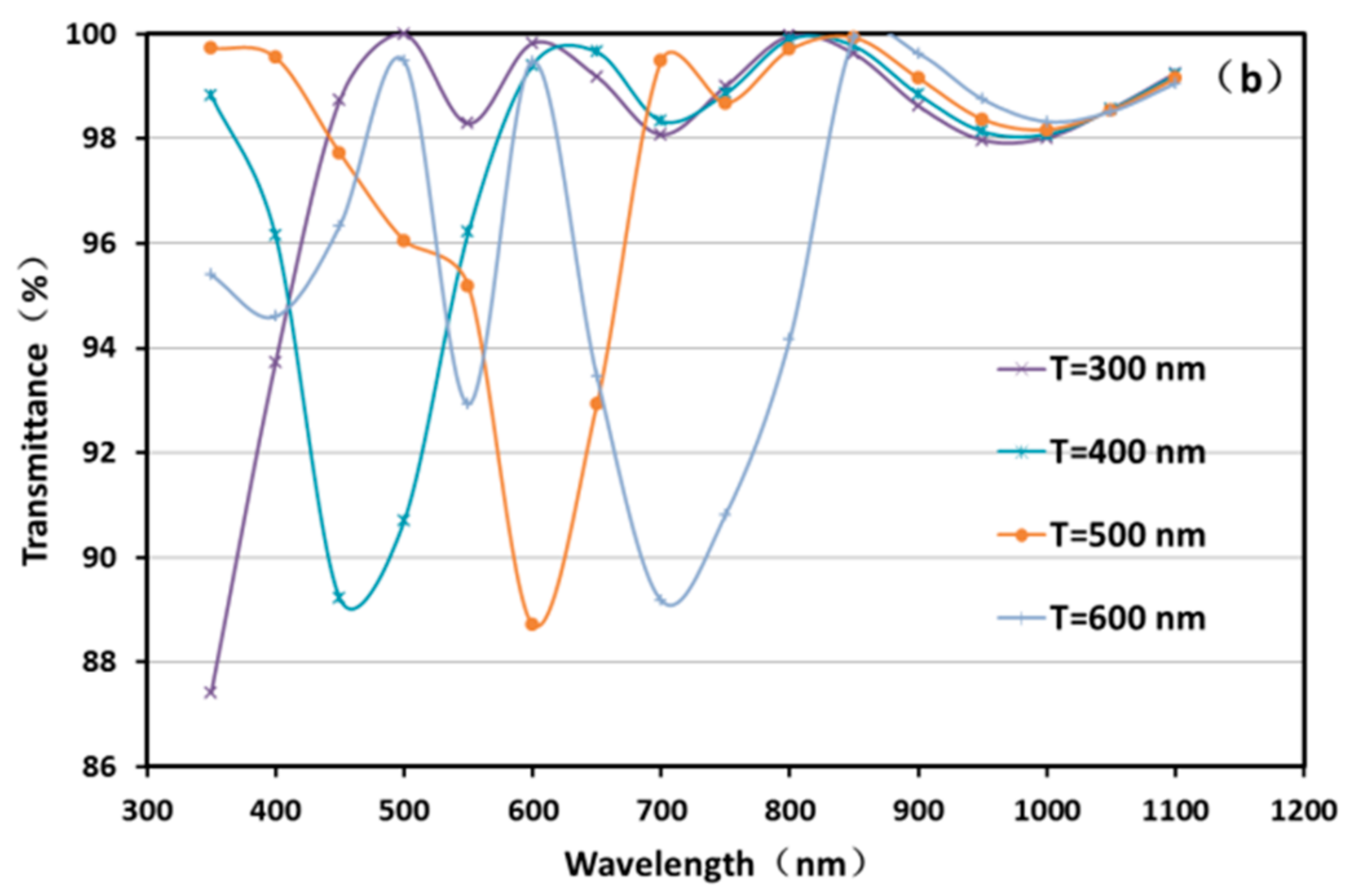
The transmittance spectra with periods of 300, 400, 500, and 600 nm are shown in
Figure 3b. Their average transmittances are 97.89%, 97.49%, 97.57%, and 96.25%, respectively, of which lowest values appear at wavelengths of 350 nm, 450 nm, 600 nm, and 700 nm, respectively. It can be seen that after
T is greater than 300 nm, the transmittance at the longwave part still maintains a high value. However, as the period increases, the lowest point of the transmittance moves toward the longwave direction, and the ratio of the period to the wavelength corresponding to the lowest point of the transmittance ranges from 0.8 to 0.9. The transmittance of the corresponding wavelength band from 350 nm to the lowest point of the transmittance is significantly reduced, resulting in an overall decrease in the average transmittance.
The grating period should be smaller than the ratio of the incident light wavelength to the substrate refractive index according to Baker’s anti-reflection condition [
19]. That is to say, when the period is larger and the incident light wavelength is shorter, the ratio of the period to the wavelength increases, approaching 1:1, and the precondition of the equivalent medium theory is not satisfied. The nanoarray layer can no longer be equivalent to an optical film but should be regarded as a rough surface with an enhanced scattering, which is not conducive to light transmission [
28]. As the wavelength increases, the ratio of the period to the wavelength decreases; thus, the period once again meets the theoretical condition of the equivalent medium, and a high transmittance can still be obtained.
Therefore, when T < 300 nm, the transmittance in the 350–1100 nm spectral range is higher.
4.2. Influence of Grating Depth on Transmittance and Optimization
From above, as the period parameter
T ≤ 200 nm, the transmittance is high, and the difference between any two spectra or two average transmittances is very small. As
T > 300 nm, the transmittance during the 350–800 nm wavelength range begins to significantly decrease. However, the 350–800 nm solar spectrum is the high-response band of most solar cells [
29]. Therefore, the period parameter is set to be 300 nm.
Set
T = 300 nm,
f1 = 0.5, and let
d =100 nm, 200 nm… 1000 nm, respectively, and calculated the transmittance spectra, as shown in
Figure 4. It can be seen that the transmittance during the 450–1100 nm band for all spectra is rather high. As
d increases from 100 to 900 nm, the number for both the peak points and valley points of the spectrum continuously reduces; finally, the spectrum is almost a straight line. This could be analyzed as follows. The same problem is still the periodic matching between the equivalent film thickness and the quarter of the incident light wavelength. The larger the film thickness is, the more times the film thickness is equal to the odd multiple of the quarter wavelength, and the more times the transmittance peak appears. Moreover, it can be seen that when
d = 100 nm, the transmittance of the 350–450 nm spectral range is also rather high, of which the value at 350 nm is up to 91.75%, but the average transmittance for the whole spectrum, 98.04%, is lower. The reason is that when the grating depth reduces, the roughness of the nanoarray structure decreases, the scattering is weakened, the transmittance of the short-wave band increases, the surface is closer to a flat film, and the effect of the nanoarray structure is significantly weakened.
According to Baker’s conclusion, the grating depth should be greater than 0.4 times the incident light wavelength [
19]. The grating depth’s adjusting is equivalent to that of the equivalent film thickness of the nanoarray layer. The matching with the equivalent refractive index should be considered for the grating depth selection. If the grating depth is too small, it loses the advantages of nanostructures for large-angle adaptation and polarization insensitivity [
19]. For
d = 300–1000 nm, the above conditions are met, as
d takes 500 nm, and the improvement of the transmittance is the most obvious. In addition, both the transmittance at the 350 nm wavelength and the average transmittance for the whole spectrum, 350–1100 nm, reach their maximum values, up to 88.91% and 98.23%, respectively. Therefore,
d = 500 nm is the optimal grating depth parameter when
T = 300 nm and
f1 = 0.5.
4.3. Influence of Duty Cycle on Transmittance and Optimization
According to the calculation results presented in
Section 4.1 and
Section 4.2, set
T = 300 nm and
d = 500 nm and optimize the duty cycle. The transmittance spectra with
f1 of 0.33, 0.5, 0.67, and 0.8 are shown in
Figure 5. It can be seen that the overall transmittance at
f1 = 0.67 is significantly improved compared with that at
f1 = 0.5. The transmittance at 350 nm has increased to 96.52%, and the average transmittance has increased to 99.21%. When
f1 = 0.33, the transmittance at 350 nm is 87.99%, and the average transmittance is 98.38%. When
f1 = 0.8, the transmittance at 350 nm is 87.71%, and the average transmittance is 98.29%. Both of them are lower than when
f1 = 0.67, and there is no obvious optimization effect when
f1 = 0.5.
Compared with f1 = 0.5, the transmittance at f1 = 0.67 increases the transmittance at 350 nm by 7.61%, and the average transmittance increases by 0.98%. The adjustment of the duty cycle is rather significant for the optimization of the transmittance. The reason is that the duty cycle adjusting is equivalent to that of the equivalent refractive index of the nanostructured layer, which directly affects the matching between the refractive index of the equivalent media film and that of the underlying substrate.
According to the Fresnel formula, the reflectivity
R0 of the uncoated substrate is
where
n0 is the refractive index of air, and
ns is the refractive index of the substrate. When a film with a refractive index of
n1 is plated on the substrate, the reflectivity
R1 of the film at the center wavelength is
where
d is the thickness of the film, and
x is the optical path. When the optical path is an odd multiple of the half-wavelength, the formula (2) is converted into
To make the reflectance of the double-layer film at the center wavelength the lowest, the following conditions must be met:
The refractive index of the equivalent media film is [
30]
where
f2 is the two-dimensional duty cycle.
The average refractive index of SiO2 is 1.47. To incorporate Equation (4) into Equation (5), the optimal equivalent refractive index of the nanostructured layer is 1.21, and the optimal two-dimensional duty cycle f2 is 0.39. Converting f2 into f1, the optimal one-dimensional duty cycle f1 is 0.63, which is very close to the optimized f1 = 0.67. This is the main reason why the transmittance is significantly improved after the duty cycle is adjusted, and it also shows that the simulation results match the theoretical calculation ones. Therefore, f1 = 0.67 is selected as the optimal parameter of the grating duty cycle when T = 300 nm and d = 500 nm.
5. Experimental Results and Analysis
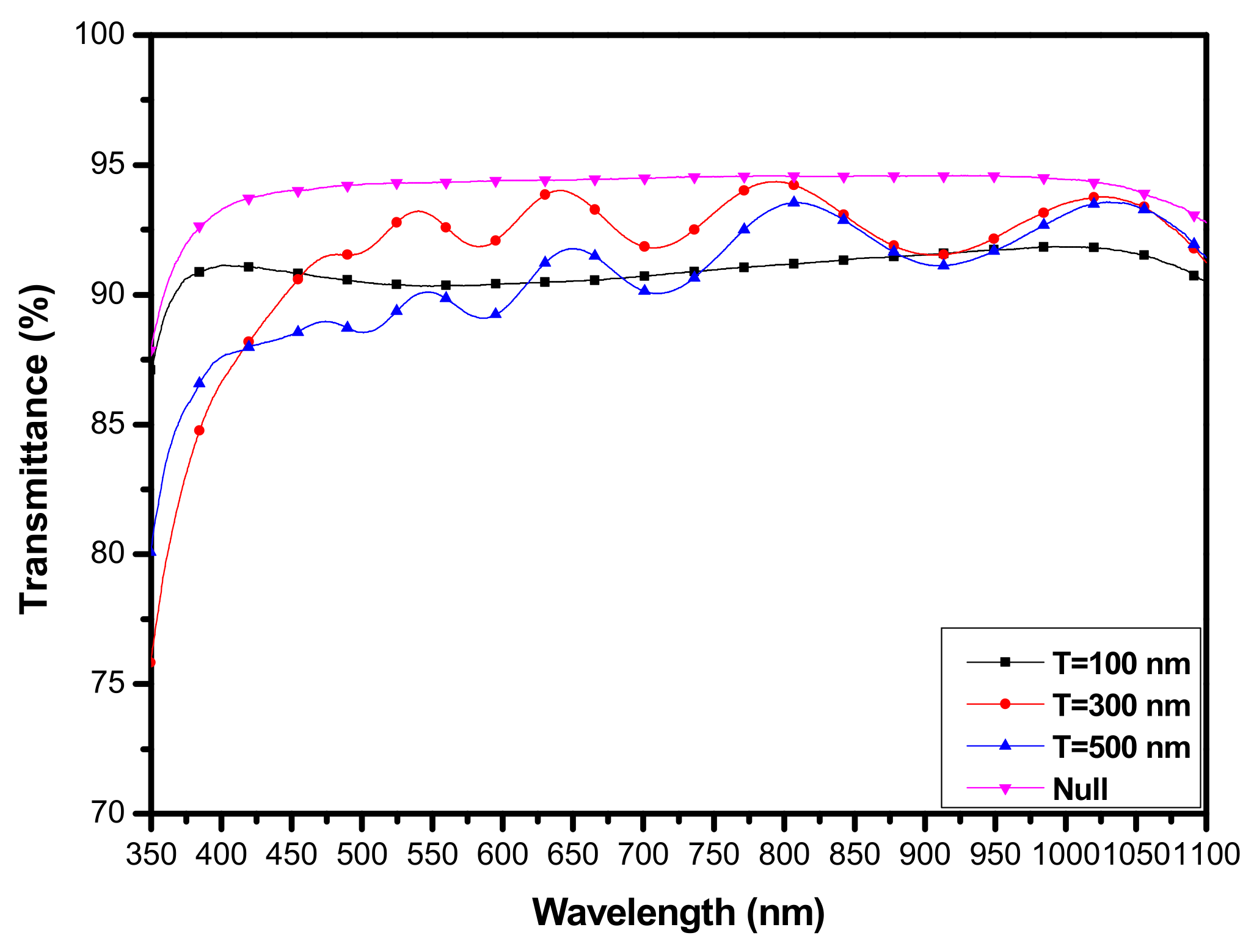
5.1. Influence of Template Cycle or Period on Transmittance
According to the numerical simulation results above, three square nanoarray imprint templates were used in this experiment work, for which the periods were 100 nm, 300 nm, and 500 nm, respectively, and the duty cycle for them all was
f1 = 50%. The transmittance spectra of the imprinted glass cover samples are shown in
Figure 6.
It can be seen from
Figure 6 that the transmittance for the 300 nm and 500 nm periods’ imprinted samples fluctuates, and the fluctuation period increases with the wavelength. The average transmittance within the 350–1100 nm band of the 300 nm period sample is 91.81%, higher than that of the 500 nm period sample, 90.75%, and that of the 100-nm period sample, 91.01%. However, the transmittance within the 350–450 nm band of the 100 nm period sample is 90.84%, significantly higher than the value of 85.84% for the 300 nm period sample and the value of 86.85% for the 500 nm period sample. In addition, the short-wave bandwidth with high transmittance is obviously extended. The results of the imprinting experiment generally conform to the simulation calculation rules in
Section 4.1.
However, the overall transmittance for all the imprinted samples is lower than that of the glass substrate. The reason is that, at this time the nanoarray structure is formed on the imprinted rubber, not on the silica, and the refractive index of the imprinted rubber (about 1.6) is greater than the refractive index of the silica (about 1.47). Therefore, the equivalent refractive index of the nanostructure layer is higher than that of the calculation model. Therefore, the transmittance regularity from the experiment conforms to that from the simulation calculation results in
Section 4.1, but the transmittance absolute value reduces. Since both the period and depth of the 100 nm period template are very small, as shown in
Figure 7a, the equivalent film thickness of the nanostructured layer of the imprinted sample must be small, which is quite different from the designed film thickness. However, the 300 and 500 nm templates have a larger period and a larger depth, as shown in
Figure 7b,c, and the equivalent film thickness of the nanostructure layer of the imprinted sample is also larger, though the difference with the designed film thickness is relatively small. Therefore, the average transmittance of the 100 nm period sample within the 350–1100 nm band is lower than that of the 300 nm period sample. Moreover, because the equivalent film thickness of the 100 nm period imprinted sample nanostructure layer is small, it could not form an odd multiple of a quarter of the incident light wavelength; since the transmittance spectrum does not form obvious peaks and valleys, there is no obvious fluctuation. In addition, the simulation conditions are more ideal than the experimental conditions (for example, the reflection of the bottom surface of the substrate is not considered), there is a difference between the simulation model and the experimental template array shape, and the imprinting process has not yet involved structural depth parameters (the equivalent film thickness has not been optimized). These are the objective reasons for the difference between the sample transmittance test’s result and the simulated nanograting structure’s result.
5.2. Influence and Optimization of Etching Time on Transmittance
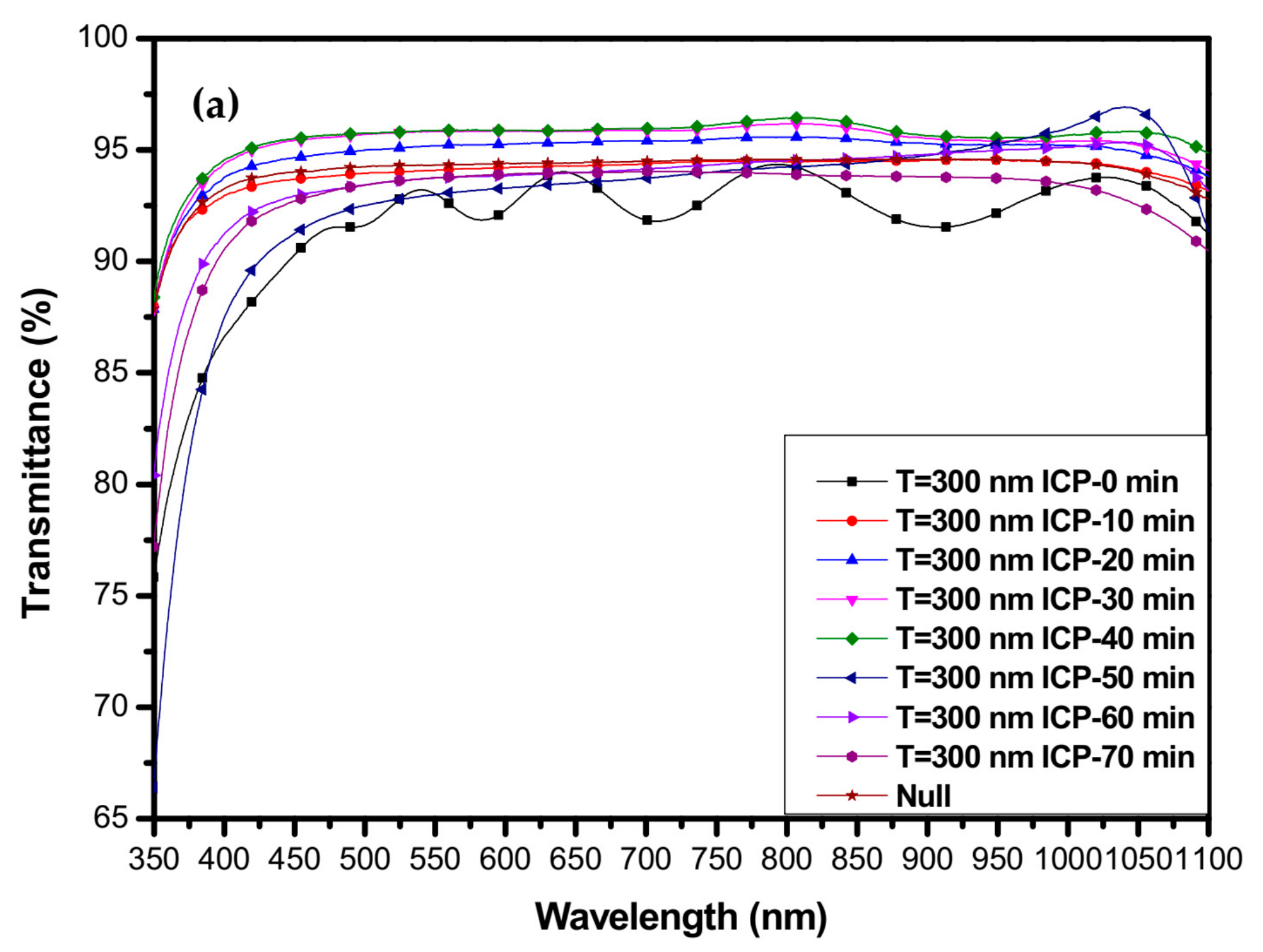
According to
Section 4.2, the 300-nm period structure sample is used as the research object in the experiment, and the plasma etching time is used to change the depth and morphology of the nanostructure. Taking 10 min as the minimum etching unit time, the samples were etched for 10, 20... 70 min, and the transmittance spectra of the samples are shown in
Figure 8.
It can be seen that the transmittance within the 350–450 nm band of each spectrum rapidly increases as the wavelength increases. In addition, the transmittance spectra within the 450–1000 nm band roughly remain parallel each other, and the transmittance remains almost unchanged. The transmittance within the 1000–1100 nm band decreases for most spectra as the wavelength increases.
The etched nanostructure is not a cylinder array like that in the calculation model. Since the upper layer is more eroded than the lower layer, the nanostructure presents a shape similar to a cone array. Therefore, the equivalent refractive index of the grating layer increases as the depth of the grating increases, and the grating layer is equivalent to an anti-reflection film with a graded refractive index. The gradual anti-reflection film is equivalent to the superposition of many thin films, and the film thickness does not meet the condition of an odd multiple of a quarter wavelength; thus, there is no fluctuation in the transmittance spectra. Since the transmittance of quartz glass within the wavelength band above 1000 nm decreases with the wavelength, the transmittance for each spectrum decreases with the increase in the wavelength, which is not directly related to the change in the nanostructure.
After 10 min of etching, the transmittance of the sample is not significantly different from that of the glass substrate. After 20 min of etching, the anti-reflection bandwidth of the 350–450 nm band begins to extend (blue shift), and the transmittance of this band increases from 92.84% to 93.36%. In addition, the average transmittance within the 350–1100 nm band is 0.79% higher than that of the glass substrate. After etching for 30–40 min, the anti-reflection bandwidth of the 350–450 nm band continues to extend (blue shift), and the transmittance of this band reaches 94.14%. The average transmittance within the 350–1100 nm band is 1.46% higher than that of the glass substrate, and the peak at the 800 nm wavelength is 1.94% higher. After 50 min of etching, the overall transmittance suddenly drops, and the transmittance within the 350–750 nm band is lower than that of the glass substrate. On the whole, the transmittance for the experimental samples conforms to the change rule from the simulation calculation results in
Section 4.2.
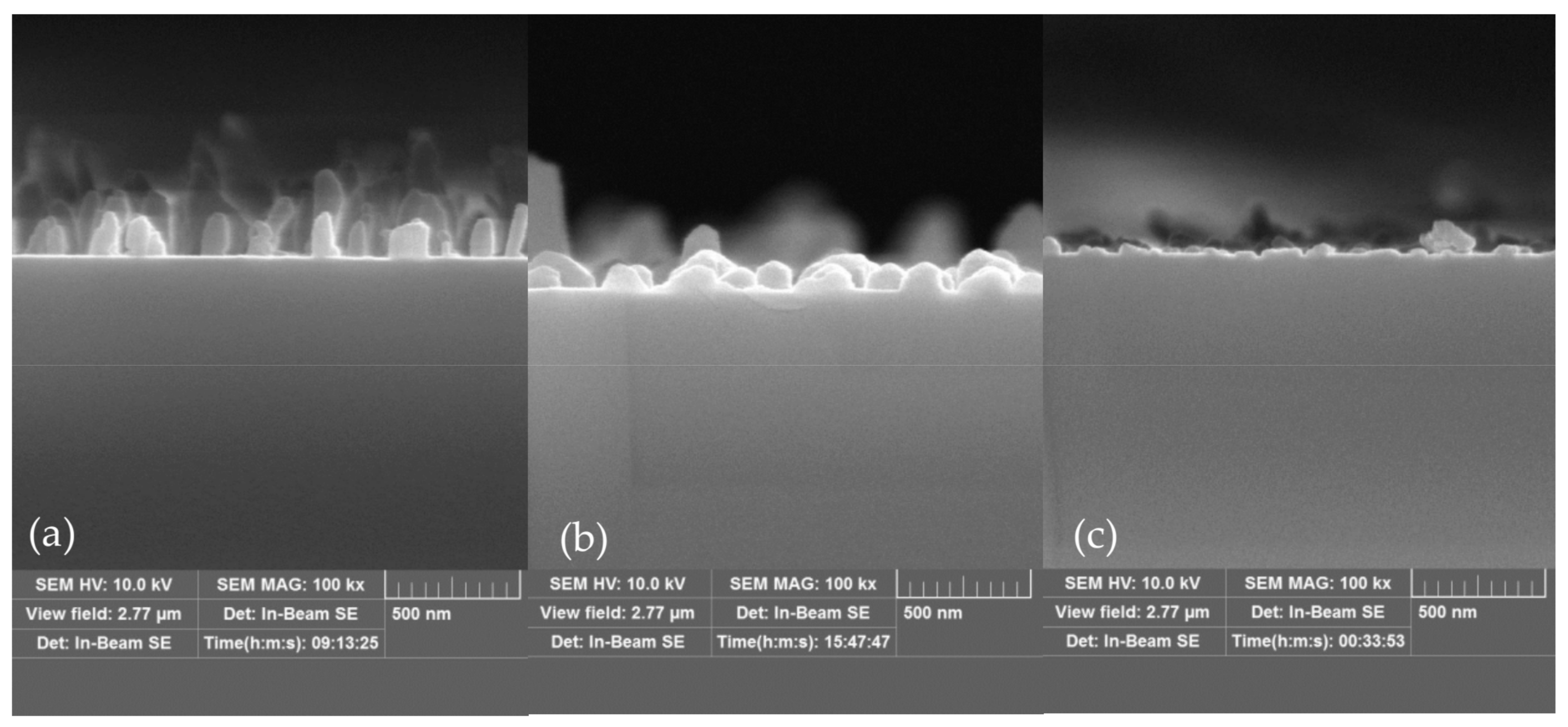
In the first 10 min of etching, the etching still basically acts on the imprinting glue, as an effective nanoarray structure has not been formed on the glass cover. The sample’s morphology is shown in
Figure 9a, so the transmittance change is not obvious. After etching for 20 min, the nanoarray structure on the upper layer of the substrate begins to form, the equivalent refractive index gradually stabilizes, the etching depth begins to increase, the equivalent film thickness of the nanostructure layer increases, and the transmittance also changes. After etching for 30–40 min, the nanostructure is relatively complete, the equivalent refractive index is stable, and the depth of the structure is 200 nm. The morphology is shown in
Figure 9b. At this time, the equivalent film thickness (structure depth) is equal to a quarter of the 800 nm wavelength, and the reflectivity is the lowest, so the transmittance peak is formed at the 800 nm wavelength. The etching time before 40 min is basically positively correlated with the depth of the structure, and the lateral etching loss is not obvious, meaning the effect of the etching on the duty cycle can be ignored. After 50 min of etching, due to the nanoarray etching reaching a certain depth and the accumulation of lateral etching loss, the nanoarray structure tends to deteriorate and begins to gradually collapse, and the periodic structure is destroyed to form an irregular surface, as shown in
Figure 9c. Both the surface equivalent refractive index and the equivalent film thickness no longer conform to the design law. At this time, the scattering of light by the rough surface increases, which is over that by a plane surface, resulting in a significant decrease in transmittance.
The effect of the etching time on the transmittance of samples with 100 nm and/or 500-nm periods also shows a similar rule, as shown in
Figure 10 and
Figure 11, respectively. After 10 min of etching, the transmittance spectrum of the sample is almost the same as that of the glass substrate. The antireflection bandwidth with the 350–450 nm band expands a little (blue shift) with 20 and 30 min etching, and the average transmittance within both 350–1100 nm and 350–1100 nm increases. However, the transmittance within 350–1100 nm significantly decreases, as the etching time is over 30 min.
For the 100-nm periodic sample, due to the small structure width, the depth that can be etched under the same aspect ratio is small, and the nanograting structure is relatively complete after 20–30 min of etching. Compared with the glass substrate, after the sample is etched for 30 min, the transmittance of the grating within the 350–450 nm band increases by 0.72%, the average transmittance increases by 0.75%, and the peak at the 800 nm wavelength increases by 0.96%. For samples with the 500-nm period, due to the larger structure width, the depth that can be etched under the same aspect ratio is larger, and the structure is relatively complete after 30–40 min of etching. When the sample is etched for 40 min, the transmittance of the grating within the 350–450 nm band is 1.34% higher than that of the glass, the average transmittance increases 1.36%, and the peak at the 800 nm wavelength increases 1.93%.
5.3. Influence of the Number of ALD Layers on the Transmittance and Optimization
According to the simulation rule in
Section 4.1, when
T is greater than 300 nm, the lowest transmittance point moves toward the longwave direction as the period increases, and the transmittance during the wavelength range from 350 nm to the lowest point significantly decreases. The overall transmittance within the 350–450 nm range of the 500-nm period sample is relatively low, which is the key point to be optimized. Since the overall transmittance of the sample etched for 20 min is relatively high, and the nanostructure is relatively complete, the experiment takes 50 layers as a unit to perform plasma-enhanced ALD on a sample with the 500-nm period and 20-min etching to change the duty cycle of the nanostructure. The transmittance spectra of the deposited samples are shown in
Figure 12.
It can be seen that the transmittance within the 350–450 nm band for all spectra rapidly increases as the wavelength increases. Within the 450–1000 nm band, the transmittance spectra remain roughly parallel, and the transmittance of each spectrum remains almost unchanged. However, the transmittance for all spectra decreases within the 1000–1100 nm band as the wavelength increases. The appearance for the transmittance spectra is basically the same as that shown in
Figure 8 in
Section 5.2, and the reason for the change is also basically the same.
After depositing 50 layers, the transmittance within the 350–450 nm band of the sample is basically the same as that of the glass, and the average transmittance within the whole band is 0.63% higher than that of the glass. After 100 layers are deposited, the transmittance within the 350–450 nm band is 1.03% higher than that of the glass, the average transmittance within the 350–1100 nm wavelength range is 2.02% higher than that of the glass, and the peak at the 800 nm wavelength is 2.66% higher than that of the glass. After 150 layers are deposited, the overall transmittance is still higher than that of the glass substrate, but it is slightly lower than that of the 100-layer sample. After 200 layers are deposited, the overall transmittance significantly decreases and gradually converges with that of the glass substrate.
Since the duty cycle of the imprinting template was only 0.5, the grating depth of the sample obviously increased after the plasma etching, but the duty cycle was basically unchanged or slightly reduced. Before 100 layers are deposited, the sample duty cycle gradually approaches the optimal calculated duty cycle as the number of deposited layers increases, as shown in
Figure 13a. The equivalent refractive index gradually approaches the calculated optimal equivalent refractive index. At this stage, the depth of the grating structure is not significantly affected. In addition, the nanostructure is relatively complete, the equivalent film thickness is relatively stable, and the transmittance increases with the increase in the number of deposited layers. The change trend conforms to the results of the simulation calculation in
Section 4.3. After 100 layers are deposited, the duty cycle continues to increase as the number of deposited layers increases, and the equivalent refractive index also continues to increase. However, because the bottom layer is thicker than the top layer, the structure morphology begins to change from the original independent cone structure into a continuous mountain-shaped structure, as shown in
Figure 13b. Moreover, the depth of the grating structure gradually decreases, the equivalent film thickness gradually decreases, and the optimization effect of the grating depth decreases; thus, the transmittance begins to decrease with the increase in the number of deposited layers. As the deposition continues, after about 200 layers are deposited, the nanoarray structure is gradually filled, and the characteristics of the nanoarray structure are gradually lost, converging with the flat film, as shown in
Figure 13c. The surface equivalent refractive index and equivalent film thickness no longer conform to the calculation rules, and the transmittance also approaches the effect of a flat film.
6. Conclusions
Based on the microstructure equivalent medium theory that is derived from the vector diffraction theory, this work established a model of the nanoarray structure grating, in which the nanostructure layer and the substrate were made of the same material SiO2, and the equivalent refractive index was adjusted with the duty cycle. Aiming at the 350–1100 nm wavelength range, the high-energy part of the solar spectrum on Mars, we simulated the influence of the nanoarray structure parameters, including the period, depth, and duty cycle, on the transmittance of the grating with G-Solver software.
The results show that: (1) The transmittance of the grating with a period of 50–200 nm is higher than that of a flat film. The lowest point of the grating transmittance spectrum moves to the longwave direction as the period increases from 300 to 600 nm, and the ratio of the period to the wavelength corresponding to the lowest transmittance point ranges from 0.8 to 0.9. In addition, the average transmittance during the wavelength band from 350 nm to the lowest transmittance point significantly reduces. (2) The depth of the grating can adjust the thickness of the equivalent medium film. When the period is 300 nm, and the duty cycle is 0.5, the depth of 500 nm is the optimal value for the transmittance. (3) The duty cycle of the grating can adjust the refractive index of the equivalent medium. When the period is 300 nm, and the depth is 500 nm, the refractive index is the closest to the theoretical optimal value if the duty cycle ranges from 0.6 to 0.7, and the transmittance significantly improves.
Nanoarray gratings were constructed on high purity quartz glass covers with nanoimprint, plasma etching, and ALD, which were used to change and control the grating structure parameters, such as the period, depth, and duty cycle through the process parameters. The experimental results of the grating transmittance support the calculation and simulation results, and they are consistent in their change trends. After the optimization of the structural parameters, the transmittance within the 350–1100 nm wavelength band of the sample with a period of 500 nm, an etching time of 20 min, and a deposition of 100 layers increased 2.02%, and the transmittance peak increased 2.66%.


