Abstract
Silicon-based thin films and nanostructures are of paramount importance in a wide range of applications, including microelectronics, photovoltaics, large area sensors, and biomedicine. The wide accessibility of silicon and its relatively low cost have driven a continuous improvement of technology based on this element. Plasma technology has been widely used for the synthesis of coatings and nanostructures based on silicon. Moreover, it has made a fundamental contribution to continuous improvement of the physicochemical properties of silicon-based materials and allows the synthesis of nanometric structures with well-defined shapes and morphologies. In this work, we have reviewed the most interesting developments in plasma-assisted processes for the synthesis of Si-based materials, both inorganic and organic, in the last five years. Special attention has been paid to new techniques, or modifications of already-existing ones, that open up new possibilities for the synthesis of materials with new properties, as well as nanostructures with novel characteristics.
1. Introduction
The development of microelectronics has given paramount importance to the study of silicon-based semiconductors. In fact, while the early development of transistor devices was based on germanium, silicon has quickly become the semiconductor of choice for the fabrication of most diffused electronic devices [1]. At present, silicon, in its monocrystalline, polycrystalline, and amorphous forms, is also of great importance for the production of low-cost photovoltaic cells, which play a primary role in the production of renewable energy [2]. Another important application of this material is in biomedicine, which may take advantage of the promising bioactive [3], antibacterial [4], and antiviral [5] properties of silicon and silicon-based alloys.
A huge amount of research has been devoted, over the years, to the study of the physicochemical properties of silicon and silicon-based materials, such as silicon oxide, silicon nitride, and silicon carbide, and the techniques for the processing of these materials, such as etching, thin film deposition, or doping, have been continuously improved [6]. Of great importance are ion implantation techniques, which have been intensively studied to modify the physical properties of silicon-based materials. Among these processes, one of the most efficient is the SmartCut method, which involves ion implantation of helium and/or hydrogen in silicon [7] to promote fracturing at a specific depth under the silicon surface in order to allow the transfer of a thin silicon layer onto another substrate [8], thus allowing the creation of a thin layer of silicon on insulator (SOI). The same implantation process has bean also studied in silicon carbide [9].
Among the different types of growth and processing techniques, plasma-assisted ones have played a major role, due to their great flexibility and ability to lower processing temperatures. As an example, plasma enhanced chemical vapor deposition (PECVD) has been intensively used for the growth of silicon-based thin films in microelectronics, photovoltaics [10], and biomedical applications [11]. Moreover, reactive ion etching (RIE) has played a paramount role for the realization of complex geometries in silicon-based devices [12]. In fact, plasma-assisted techniques are able to activate chemical reactions at low temperatures, enabling the production of ions, atoms and radicals, that can be employed for the modification of surface morphologies and for the synthesis of thin films and nanostructures [13].
In this work, we report the most interesting developments in the field of plasma-assisted techniques for the synthesis of silicon-based thin films and nanostructures, as well as for the modification of surfaces containing silicon, in the last five years. The research has been carried out using the Scopus and Web of Science databases, limiting the research to publication years between 2018 and 2023, although in some cases older sources have been included if a more detailed explanation of a technique that was briefly described in another paper was presented. A preliminary selection of the papers was carried out by carefully reading the abstracts; then the selected papers were carefully evaluated, taking particular care when considering the experimental sections. Only experimental works that involved the synthesis or the surface modification of silicon-based materials by means of plasma-assisted techniques have been included in the review. Studies in which silicon-based materials were used only as substrates for the growth of other materials have not been included, unless a functional role was exerted, such as in the case of adhesion improvement layers. Materials in which silicon was used only as a dopant have been excluded as well. The discussion has been divided in two parts: the first is dedicated to techniques that work at pressure lower than atmospheric, thus requiring the use of vacuum technology, while the second deals with techniques that work at atmospheric pressure. A special focus has been given to unusual applications of plasma discharges for the synthesis of silicon-based materials with special properties. The general organization of the review work is shown in the schematic representation given in Figure 1, while the detail of the low-pressure techniques categorization is given in a separated scheme in Figure 2.
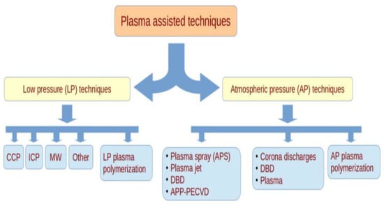
Figure 1.
Schematic representation of the review: the plasma-assisted synthesis techniques have been categorized first by the working pressure and then divided respect to the working principle.
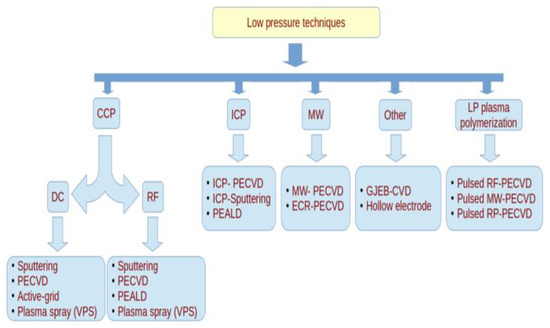
Figure 2.
Schematic representation of the low-pressure technique descriptions, which have been categorized respect to the type of energy source used, but a separate part has been devoted to plasma polymerization.
2. Synthesis by Means of Low Pressure Discharges
Low-pressure discharges have been used for more than three decades for the synthesis of several types of silicon-based thin films, especially for applications in the fields of microelectronics, large area electronics, and photovoltaics. Radio frequency, capacitively coupled plasma-enhanced chemical vapor deposition (RF-PECVD), and sputtering, with several variations, have been the most commonly used techniques, due to their high flexibility, but several other types of plasma-assisted techniques have been developed, including the use of inductively coupled plasmas (ICP), hollow cathode/anode plasmas, microwave plasmas, and electron cyclotron resonance (ECR) discharges. In this section, the most recent developments in low-pressure discharges for silicon-based materials are reviewed, dividing the techniques respect to the type of excitation used to produce the plasma discharge, as shown in Figure 2: capacitively coupled direct current (DC) and radio-frequency (RF), inductively coupled (ICP) or microwave (MW) discharges, as well as other discharges, which do not belong to the previous categories. A separated paragraph is dedicated specifically to the synthesis of polymer-like coatings.
2.1. CCP-DC Discharges
Low-pressure plasma discharges activated by means of a DC bias rely on the application of a static electric bias between two electrodes for the activation of the plasma discharge. In the simpler configuration, the two electrodes are planar and parallel with respect to one other, but several other configurations are possible, such as cylindrical coaxial electrodes. In this kind of discharge, the secondary emission of electrons from the cathode, as a result of the interaction with positive ions approaching its surface, is usually important for maintaining the discharge balance [13]. Compared to techniques in which RF activation is used, a higher voltage is usually necessary, and a considerable ion bombardment is often exerted on the substrate surface. These processes are usually less expensive compared with the ones activated by RF bias, since the latter typically require a more expensive generator, as well as the use of a matching network to prevent or limit the reflected power [13]. However, despite the lower cost, the use of DC-activated discharges is less common due to their lower versatility compared to RF and the limitations concerning the use of insulating electrodes, related to the problem of surface charging. Moreover, these processes typically involve a strong ion bombardment on the substrate and the growing film, which may be detrimental to the film’s properties in some cases, e.g., by increasing the formation of defects in semiconductor materials.
Despite intrinsic limitations, DC discharges are quite often used for the deposition of carbon-based materials, such as diamond-like carbon (DLC) or carbon nanotubes (CNTs). In fact, these techniques can create high electron energy, which is necessary for the dissociation of gases with strong molecular bonds, such as CH4, that are often used for the synthesis of these materials. In this context, an interesting study was carried out by Delfani et al. [14] to investigate the effectiveness of silicon-based thin films such as a-Si:H, a-SiC:H, and a-SiN:H, deposited by means of pulsed DC-PECVD, to enhance the adhesion of DLC thin films on steel substrates. The Si-based layers and the DLC coatings were grown in succession in the same deposition chamber by means of a pulsed DC discharge, analyzing the effect of substrate temperature on the adhesion strength of the DLC films in particular. The authors found that a-SiN:H films grown at temperatures higher than 150 °C provided the best results in terms of adhesion with the DLC films.
Silicon-based interlayers of carbon-based materials were also studied by Lakhonchai and coworkers [15], focusing on the corrosion resistance of hydrogenated amorphous carbon (a-C:H) thin films grown on chromium-plated substrates, which were coated with a-Si, a-Si:N, a-Si:H, and a-SixCy:H layers. In this case, the silicon-based layers, as well as the a-C:H films, were grown by means of a hybrid PECVD/DC-sputtering deposition system, in which Ar, H2 and C2H2 were introduced in different amounts depending on the material to be grown. The structure of the hybrid PECVD/sputtering reactor is depicted in Figure 3, where the location of the substrate holder and of the sputtering source are visible. In this study, the authors found a-Si:H interlayers more effective for improving the adhesion of the carbon-based films, compared to the other silicon-based materials investigated, while the worst behavior was observed in the a-SixCy:H material.
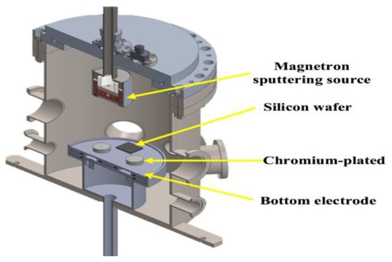
Figure 3.
Structure of a hybrid PECVD/sputtering apparatus used for the deposition of a-C:H thin films and Si-based interlayers for improving adhesion to steel. Reprinted from [15].
Silicon-carbon hybrid materials show interesting properties for the production of anodes for lithium-ion batteries with enhanced stability, as was recently investigated by Sun and coworkers [16]. In this study, active screen plasma was used for the deposition of SiOx/C nanostructured materials by dispersing ordered mesoporous carbon (CMK3) on a silicon substrate and then activating discharge at low pressure in a H2 atmosphere. In accordance with the active screen process, the DC bias was applied between the chamber walls and an active screen mesh (ASM), composed of a metal grid that surrounded the substrate, as shown in the schematic representation of Figure 4. The plasma discharge produced radicals that were able to reach the substrate by diffusing through the ASM, while the ion bombardment impinged on the mesh that protected the substrate from it. Such a configuration allows the use of a DC discharge while strongly reducing substrate and film damage by the ion bombardment. The process resulted in the formation of nanostructures of different shapes, composed of a mixture of SiOx and amorphous carbon, that displayed interesting properties for the production of battery anodes.
Figure 4.
Scheme of the deposition of silicon-based nanostructures by means of an active-screen DC plasma reactor. The active screen mesh surrounding the sample holder is visible in the middle of the graph. Reprinted from [16] with permission from Elsevier.
Silicon-carbon based materials are also suitable for biomedical applications, as in the case of the recent studies by Grenadyorov and coworkers, which were focused on the use of a pulsed DC-PECVD discharge for the synthesis of hybrid a-C:H:SiOx materials onto Ti–6Al–4V alloy substrates. The hybrid deposition system employed both a pulsed DC generator and a hot filament to achieve the dissociation of the polyphenylmethylsiloxane (PPMS) vapor used as precursor [17]. The a-C:H:SiOx layers showed good mechanical properties [17], good biocompatibility and adhesion, and high wear resistance [18], making these materials good candidates for application to biomedical devices.
Plasma spray is a kind of physical vapor deposition (PVD) technique, often used in applications where thick and porous coatings are required, such as in thermal insulation and some kinds of biomedical surfaces. In this process, a powder precursor is injected into a flow of plasma, melted or evaporated, and then transported to the substrate, where it typically adheres in the form of microlamellae. The technique can be carried out at atmospheric or reduced pressure, depending on the application, and the flow of plasma can be excited by a DC or RF bias. An original type of hybrid DC/RF plasma spray at low pressure was used by Ohta and coworkers [19] for the production of silicon nanoparticles (Si NPs) intended for use in the fabrication of cathodes for lithium-ion batteries. The system employed a plasma torch in which both DC and RF excitations were applied to generate the plasma, with a specific design that allowed the precursor powders to be injected directly into the hotter plasma zone, allowing for a more efficient evaporation and better plasma stability. A considerable production rate of 17 g min−1 was obtained under optimized conditions, with an average nanoparticle diameter of 50 nm. Plasma spray was also used by Harder [20] for depositing Si-HfO2 coatings onto SiC substrates, with the aim of protecting the materials against oxidation in a steam environment. The same plasma torch, working at a pressure of approximately 1 Torr, was used to achieve the formation of a double layer in which the basecoat was composed of Si-HfO2 and the topcoat of Yb-silicate EBC, although the author found that the coating’s resulting effectiveness limited.
2.2. CCP-RF Discharges
Low-pressure capacitively coupled radiofrequency (CCP-RF) discharges are the most common type of applications of cold plasmas and, being very versatile, are used in a wide range of applications. Among these techniques, RF-PECVD and RF magnetron sputtering [13] are in very common use thanks to the ability of these techniques to grow a large number of materials, including silicon-based ones, on substrates of different types, including plastic materials, and to achieve high control of material stoichiometry during the synthesis of alloys. These techniques require the use of RF generators, which are often more expensive than DC ones, and matching networks, which are used to tune the impedance of the load coupled with the generator, with the aim of minimizing the amount of power reflected to it. The use of RF bias provides a greater versatility, allowing for deposition on insulating substrates and reducing the amount of ion bombardment on the surface of the substrate and the growing film, which is detrimental in some applications.
The RF-PECVD technique is also called plasma-assisted chemical vapor deposition (PACVD) and usually, if not specified otherwise, involves the use of capacitively coupled plasma (CCP) generated by the application of a radiofrequency bias between two planar electrodes. Nonplanar configurations and inductive coupling are also possible but less common. The most common choice for the excitation frequency is 13.56 MHz, which is an industrial standard for RF generators. Since this frequency value lies between typical electron and ion plasma frequencies, it allows a separation between the behavior of the two particles [13]. Higher frequencies, such as 40 MHz or 75 MHz, are also used in order to achieve specific material properties, and in this case the technique is often called very high frequency PECVD (VHF-PECVD).
One of the most typical applications of RF-PECVD is the growth of amorphous silicon-based materials [21], such as a-Si, a-SiOx, a-SiNx, a-SiCx, a-SiOxCy, a-SiOxNy, and even a-SiCxOyNz [22], the compositions of which can be tuned efficiently by controlling precursor gas concentrations. In recent years, great interest has been dedicated to the application of PECVD techniques for depositing silicon-based amorphous thin films for the passivation of silicon heterojunction photovoltaic cells (SHJ), which are considered very promising for improving the efficiency of solar energy-production devices. These cells usually involve the deposition of an intrinsic amorphous silicon thin film on a crystalline silicon substrate, followed by the growth of a doped amorphous silicon layer.
Ruan and coworkers [23] fabricated SHJ solar cells, employing a standard RF (13.56 MHz) plasma to excite a mixture of silane (SiH4) and hydrogen (H2) for the deposition of intrinsic a-Si:H passivating layers onto the crystalline silicon cell layer. A VHF excitation (40.68 MHz) was used instead for growing the doped a-Si:H layers of the cells. The effect of substrate temperature on the quality of the passivating layers was investigated especially closely, and a maximum cell efficiency of 23.3% using layers grown at 210 °C was achieved.
The deposition of a-Si:H on black silicon (b-Si), which is a crystalline silicon material with a surface nanostructured to achieve a very low reflectivity, was studied by Ozkol and coworkers [24] for the fabrication of SHJ cells. The deposition conditions at standard RF excitation (13.56 MHz) and very low power (13 mW cm−2) were investigated, using a mixture of silane and hydrogen in order to achieve a conformal deposition on the highly structured black silicon surface.
In addition, Sai and coworkers [25] studied the deposition of a-Si:H layers on crystalline silicon to achieve good passivation properties, but in this case, mixtures of silane and disilane (Si2H4) were used, with variable proportions of the two silicon precursors, in a standard RF (13.56 MHz) PECVD reactor. The effect of the plasma composition, pressure, and substrate temperature on the microstructure of the a-Si:H layers was investigated. The obtained a-Si:H layers did not show good passivating properties as standalone coatings, but the performance of the films increased substantially when using bilayers of different densities, with a more porous layer with a thickness of 2 nm grown on c-Si and then coated by a denser layer with a thickness of approximately 8 nm.
Wang and coworkers [26] compared the effectiveness of a-Si:H passivating layers grown by PECVD from silane using RF (13.56 MHz) and VHF (40 MHz) plasma excitation frequencies on a large area (about 1 m2). A higher performance of the former compared to the latter was found, especially due to the formation of a very thin epitaxial layer at the c-Si/a-Si:H interface, when the amorphous layer was grown using a VHF excitation. According to the authors’ conclusions, however, it should be possible to improve the deposition conditions of VHF-grown film to improve the film quality.
The effect of gas flow rate on the passivation quality of a-Si:H layers grown by PECVD was studied by Pandey and coworkes [27], employing a PECVD reactor with RF (13.56 MHz) excitation and a mixture of silane and hydrogen in equal proportions (SiH4/H2 = 1) to grow a-Si:H layers on c-Si using variable flow rates.
Of particular interest is the study by Ouaras and coworkers [28], aimed at the development of a novel type of PECVD reactor with interdigitated electrodes, by which a patterned deposition of a-Si:H was performed on a solar cell of area 156 mm × 156 mm, without the need for a lithographic step. The reactor, a scheme of which is reprinted in Figure 5, consisted of a hollow steel electrode, connected to the RF (13.56 MHz) generator, one face of which was structured with a set of slits. An insulating layer surrounded the electrode, preventing the formation of parasitic plasma discharges with the grounded metal walls. The top plate of the patterned electrode had 66 rectangular slits, each one having a width of 1 mm and a length of 130 mm. The set of slits faced the grounded electrode, on top of which the substrate was positioned. With careful study of the process parameters (pressure, flow rates, distance between the slits and the grounded electrode), a set of localized discharge could be achieved, allowing for a selective deposition on the substrate.
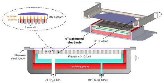
Figure 5.
Schematic of the interdigitated electrode used for the patterned deposition of a-Si:H on solar cells, allowing for the formation of patterns without the need for lithographic step. Reprinted from [28] with permission from Elsevier.
The group of Chen and Truong studied a different approach for the passivation of crystalline silicon [29]. In this case, a wet chemical process was applied to achieve the formation of a thin (1.4 nm) SiOx layer on the top of the c-Si wafer, then a hybrid dual-mode PECVD was used for the deposition of a-Si passivating layers on the oxidized silicon. The deposited Si layers were then doped by diffusion. The RF/MW PECVD reactor employed the synergistic action of microwaves (2.46 GHz) and radiofrequency (13.56 MHz) excitation to form a plasma discharge in a mixture of silane and argon. The authors also compared the passivation effectiveness of Si films grown by RF/MW PECVD with the same materials grown by sputtering and LPCVD [30].
Silicon-based nanoparticles, as well as nanocrystalline materials, in which nanocrystals are usually embedded in an amorphous matrix, are interesting for several applications, including solar energy production, and PECVD is a very common way to synthesize these structures. In fact, in recent years, several research groups carried out studies on the use of RF-PECVD techniques for the synthesis of nanocrystalline silicon-based materials and nanoparticle-based materials. In most cases, a standard RF-PECVD system with parallel-plate electrodes was used to synthesize the material, but careful study of the process parameters, especially precursor dilution and power density, was usually required to achieve good control of the material properties.
Wang and coworkers [31] studied the effect of pressure in the deposition of nanocrystalline silicon (nc-Si) by RF-PECVD, using a mixture of silane and hydrogen. The authors investigated an unusually wide range of pressure values (150–1050 Pa) in order to understand how the tuning of this parameter could be used to improve hydrogen incorporation in the material and found an optimal value of 450 Pa. In fact, the incorporation of hydrogen is usually considered a method to reduce defect density in amorphous and nanocrystalline silicon to improve its electrical properties.
Sharma and coworkers [32] performed a study on the effect of RF power during PECVD deposition on nanocrystalline silicon using a mixture of silane and hydrogen. In this work, it was found that, in a particular power range, it was possible to obtain a material with specific characteristics, called sub-nanocrystalline silicon, with intermediate properties between the amorphous and the nanocrystalline structure.
The transition between amorphous and nanocrystalline silicon structure was investigated by Wang and coworkers [33] as well, using a standard RF-PECVD. However, unlike most other groups, trichlorosilane (SiHCl3) was used instead of silane as a silicon precursor gas. Optical emission spectroscopy (OES) was also employed to investigate the plasma composition at different values of the process parameters (pressure, RF power, and gas flow rate), and a correlation was found between some characteristics of the plasma emission spectrum and the transition between the amorphous and nanocrystalline deposition regimes.
Plasma-assisted surface modifications have also been used to achieve the production of silicon-based nanocrystalline materials. In the work of Ghosh and coworkers [34], an a-SiN layer was grown on the rear of crystalline silicon PV devices by means of a standard PECVD process, and SiN nanoparticles were subsequently produced by hydrogen plasma etching. The nanostructures were then embedded in a-Si:H layers, which were grown using the same reactor. The plasmonic properties of SiN nanoparticles were exploited to improve the optical behavior of the cell.
The standard RF-PECVD process was also used for the synthesis of multilayer structures with alternating layers of silicon nanocrystals and silicon oxide, intended for application in photonic devices. Chen and coworkers [35] created multilayers of boron-doped silicon nanocrystals (SiNC) alternating with amorphous silicon oxide using the following procedure. A layer of B-doped a-Si:H was first deposited by means of a standard PECVD process, using a mixture of silane and diborane (B2H6), then a plasma oxidation process was applied to form a a-SiO2 layer. The synthesis of this two-layer structure was repeated 15 times. The multilayer was then dehydrogenated at 450 °C and annealed at 1000 °C in order to promote Si segregation in the a-Si layers to form the Si nanocrystals. In addition, Shibata and coworkers [36] used the same type of procedure for the fabrication of SiNC/a-SiO2 multilayers, involving the deposition of a-Si:H/a-SiO2 structures followed by high-temperature post-deposition treatment. However, an unusual plasma excitation frequency of 27.12 MHz was used during the PECVD deposition processes, and the work was focused specifically on the thermoelectric properties of the multilayer structures intended for thermoelectric applications.
The PECVD growth of microcrystalline and polycrystalline silicon layers was also investigated by several research groups. Li and coworkers [37] used a VHF (75 MHz) excitation frequency PECVD system for growing intrinsic mc-Si layers on glass substrates, investigating the effect of deposition rate on the film microstructure. The deposition system, a scheme of which is reprinted in Figure 6, was equipped with an in situ optical emission spectroscopy (OES) apparatus, which allowed an analysis of the plasma composition during the growth process. The authors studied the effect of the deposition rate on the evolution of the SiH radical concentration over time. Moreover, Liu and coworkers [38] achieved the synthesis of polycrystalline silicon thin films on polymeric substrates at a temperature of 100 °C by means of a RF-PECVD system. In order to promote film crystallization, a variable DC negative bias was applied to the substrate to achieve a tunable ion bombardment. A transition between amorphous and polycrystalline structure was obtained for biases higher than 50 V, and the optimal bias value was obtained at 100 V, over which a degradation of the film structure was observed.
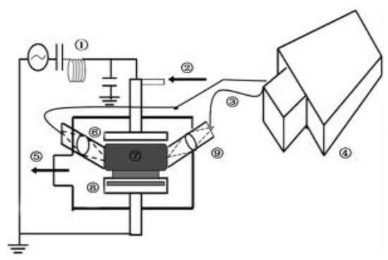
Figure 6.
Schematic representation of a RF-PECVD system used for the deposition of intrinsic mc-Si layers, equipped with an in situ OES analysis system. Reprinted from [37] with permission from Elsevier.
The synthesis of silicon-based ternary compounds is another interesting application of RF-PECVD techniques, which allows for fine-tuning of the elements incorporated into the material, thanks to the possibility of tuning the amount of precursor radicals in the plasma discharge by regulating gas flow rates and RF power [21]. Song and coworkers [39] investigated the growth of silicon-carbon-oxygen amorphous ternary alloys (a-SiCxOy), doped with nitrogen, with a specific focus on the photoluminescence properties of these materials. A VHF-PECVD reactor was used, although the exact excitation frequency was not specified in the work. The grown films showed photoluminescent properties in the red, orange-yellow, white, and blue regions. Hang and coworkers [40] studied the growth of silicon-nitrogen-oxygen amorphous ternary alloys (SiOxNy) by means of standard RF-PECVD and demonstrated the possibility of tuning the refractive index of the films, obtaining a value between 1.49 and 1.66 at a wavelength of 550 nm, thus allowing the fabrication of optical filters. Ke and coworkers [41] investigated the deposition of silicon-boron-nitrogen amorphous alloys (a-SiBzNy) on steel for mechanical applications, using a standard PECVD parallel-plate reactor with an unusual plasma excitation frequency of 2 MHz. According to the authors’ conclusions, the incorporation of boron produced an increase in the mechanical properties of the film, compared to those of a-SiNx.
Silicon-based nanowires (NWs) are another material which was effectively grown by means of PECVD techniques. Recently, silicon NWs of lateral dimensions as low as 6 nm were grown by Wang and coworkers [42] using a standard RF-PECVD reactor and a mixture of silane and hydrogen after having prepared the substrate with mixed catalyst of Sn and Cu. The authors found that during exposure to the atmosphere of the as-grown Si NWs, an oxidation process could naturally take place, leading to the formation of silica nanowires on the top of the fabricated structures.
Silicon-tin NWs were also grown by Azrak and coworkers [43] using a procedure called in-plane solid–liquid–solid (IPSLS), which included the use of tin (Sn) as catalyst and the deposition of a-Si:H layers by means of a RF-PECVD reactor. The method presented by the authors involved the evaporation of a thin Sn layer with a thickness of approximately 30 nm, which was then patterned by a lithographic process to form strips of 5 µm lateral dimension and etched by H2 plasma to remove any oxidation layer and form Sn nanoparticles. An a-Si:H thin film of about 30 nm was then grown on the top of the strips by conventional PECVD at a temperature of 120 °C. The material was then annealed at 200–300 °C to activate the growth of the nanowires. At the end of the process, SiSn NWs were grown in-plane (parallel to the substrate surface) and incorporated an amount of Sn between 9% and 10%, depending on the annealing temperature. The authors demonstrated the use of the SiSn NWs in the fabrication of bottom-gate field-effect transistors (FET).
Atomic layer deposition (ALD) is a technique which relies on the alternating injection of different precursors into the reaction chamber, employing specific and highly selective chemical reactions to form extremely conformal alloy coatings with thickness control at the atomic level. Its variant called plasmaenhanced ALD (PEALD), which is also called time-modulated PECVD, employs the use of a plasma discharge to produce radicals that are then injected into the reaction chamber to be used in the chemical reactions, increasing the technique versatility. This technique has risen in importance with the continuous increase of complexity of nanodevices, the fabrication of which often requires covering conformal surfaces with very small features such as pores or spikes and the deposition of layers with nanometric thickness.
Recently, Baranov and coworkers studied the growth of GaP/Si superlattices for photovoltaic applications, with GaP layers with a thickness of 3 nm and Si layers with a thickness of 0.5 nm [44] or 1.5 nm [45]. The authors used a hybrid deposition process that employed a standard RF-PECVD in continuous mode for the deposition of the microcrystalline silicon (mc-Si) layers and a PEALD using trimethylgallium (TMG) and phosphine (PH3) for growing the crystalline gallium phosphide (GaP) layers. The obtained superlattices resulted in a pure crystal structure without an amorphous phase. The authors proposed the application of the superlattices to making the upper junction of multijunction solar cells based on III−V/Si.
Radio frequency-activated sputtering has been used for the deposition of silicon-based materials in recent years. As an example, an interesting study by Zhang and coworkers [46] studied the incorporation of deuterium into silicon carbide thin films grown by means of a conventional RF sputtering system, the scheme of which is reprinted in Figure 7, using an atmosphere of deuterium gas. The films were designed for use as plasma-facing material (PFM) in nuclear fusion reactors and were composed of a mixture of Si- and C-deuterated nanoparticles embedded in a disordered a-SiC matrix.
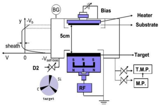
Figure 7.
Structure of the RF−sputtering system used for the deposition of silicon carbide thin films with deuterium incorporation. Reprinted from [46] with permission from Elsevier.
A simple O2 RF plasma activation of 1.4404 stainless steel parts through a radical polymerization of N-vinylpyrrolidone, industry-relevant as components of microreactors for the production of PVP in aqueous solution, was applied [47] for the deposition of an ultra-thin 1H, 1H, 2H, 2H perfluorooctyltriethoxysilane (FOTS) antifouling coating. Compared to the standard sol-gel method (precursors: FOTS and Zirconium(IV)-acetylacetonate (Zr(acac)4), the plasma-assisted process showed outstanding anti-adhesive properties with almost no PVP deposit formation on the steel components, though the surface roughness remained higher.
Another comparative study involved (3-aminopropyl)trimethoxysilane (APTMS) [48] (structure formula is reported in Figure 8b) as a grafting molecule for a type of cross-linked polyethylene which is produced through the silane method, generally known as organosilane-grafted moisture-crosslinked polyethylene or silane-crosslinked polyethylene (Si-XLPE) (Figure 8a), compounds that are widely used in the electrical and biomaterials industries and can be improved by the integration of trifunctional organosilanes, such as APTMS. Indeed, this molecule is capable of polymerizing in the presence of water, which gives rise to a different possible configuration structure based on 2-dimensional and 3-dimensional surface-induced polycondensation through covalent attachment.
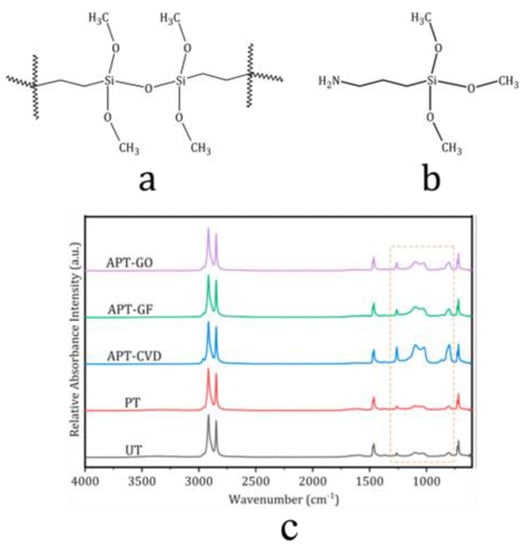
Figure 8.
Chemical structure of (a) Si−XLPE and (b) APTMS; (c) ATR−FTIR spectra of untreated (UT), plasma-treated (PT), APTMS chemical vapor−,deposited (APT−CVD), APTMS plasma grafted from (APT−GF), and APTMS plasma grafted onto (APT−GO) samples. The dashed area had the most noticeable variations. Reprinted from [48] with permission from Elsevier.
Chemical vapor deposition (CVD) and plasma-facilitated in situ grafting methods (grafting-from and grafting-onto) were employed to immobilize APTMS. The reactor for the plasma-assisted processes was a low-pressure plasma system operating at a maximum power of 100W and low frequencies (40–100 kHz). The characteristics of obtained samples with the same main preparation principles were compared to each other in terms of surface chemistry (XPS, EDX, and ATR-FTIR-related spectra are compared in Figure 8c), morphology (by AFM and FESEM), and wettability (by contact angle measurement), thus showing that the plasma grafting-from deposition method favored the highest attachment of APTMS to the surface by forming multilayer structures instead of monolayers and leading to the creation of hydrophobic surfaces.
2.3. ICP-RF Discharges
Inductively coupled plasma (ICP) discharges employ the generation of a time-varying magnetic field by means of an alternating current flowing in one or more coils, which in turn provides the generation of a variable electric field able to accelerate electrons and ions to generate a plasma discharge [13]. Compared with CCP discharges, ICP ones typically provide a higher plasma density and have the advantage to avoid the ion bombardment, due to the absence of sheaths. However, when an ion bombardment is required to achieve specific effects during the process, it can be obtained by adding a DC or RF bias to the sample surface, the intensity of which can be tuned as required. ICP discharges have been used in recent years to grow silicon-based materials by means of PECVD, PEALD, and sputtering processes.
Rumyantsev et al. [49] employed an ICP-PECVD reactor to achieve the synthesis of amorphous hydrogenated silicon-carbon (a-SiCx:H) and silicon-carbon-nitrogen (a-SiCxNy:H) alloys from tetramethylsilane (TMS, Si(CH3)4), plus nitrogen for N-containing films. The plasma was excited inductively using a frequency of 13.56 MHz, and the external surfaces of the vacuum chamber were plated with permanent magnets to improve reactor efficiency. The authors found that substrate temperatures ranging from 100–500 °C and TMS partial pressure exerted a very limited effect on the optical properties of the films and concluded that the ICP was able to maintain uniform deposition conditions on the substrate surface, regardless of the change in partial pressure and temperature. Yang and coworkers [50] investigated the use of an ICP-PECVD technique for the synthesis of silicon dioxide and silicon thin films at very low temperatures (20 °C), using silane (SiH4) and oxygen as precursor gases. The fabrication of metal-oxide-semiconductor (MOS) and thin film-transistor (TFT) devices was demonstrated, achieving a breakdown field of 9 MV cm−1 and a flat-band voltage of −0.6 V.
A variant of the PEALD techniques involves the use of ICP for the formation of the required radicals and was recently employed for the synthesis of silicon nitride and oxinitride as well as silicon dioxide. In fact, Song and coworkers [51] used a multi-ICP system with seven coils connected in parallel, the scheme of which is reprinted in Figure 9, to generate N radicals to be incorporated into SiN and SiCN alloys. The high-power plasma produced by the coils reached an electron density of 1018 m−3 and resulted in a nitrogen incorporation as high as 28%.
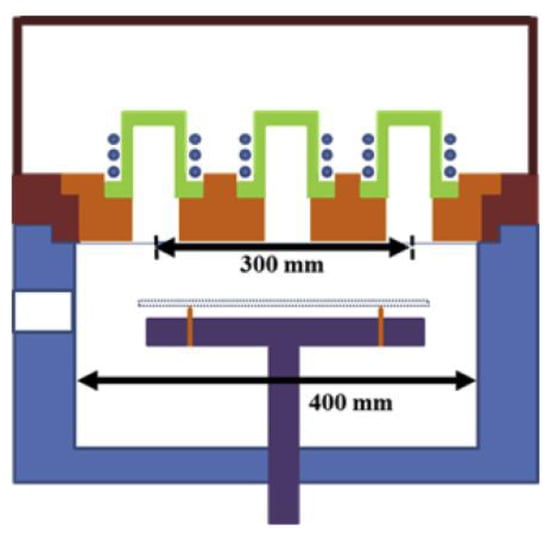
Figure 9.
Scheme of the ICP-PEALD reactor with 7 coils, used for the deposition of SiN and SiCN thin films. Reprinted from [51] with permission from Elsevier.
Jung and coworkers [52] employed a remote ICP for the growth of SiO2 layers from bis(tertiary-butylamino)silane (BTBAS) and oxygen. The films were grown at substrate temperatures between 300 °C and 400 °C and showed a breakdown field as high as 10.5 MV cm−1.
Takenaka and coworkers [53] employed an ICP sputtering system, in which low-inductance antenna (LIA) modules were arranged near rectangular silicon sputtering targets, as shown in the scheme reprinted in Figure 10, to produce an intense and homogeneous ion bombardment, resulting in the deposition of Si thin films with crystallinity in the range between 73–78% without intentional substrate heating. The innovative process is especially interesting for the deposition of silicon on plastic materials, which are not able to resist high temperatures.
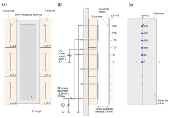
Figure 10.
Schematic representation of the sputtering system used for the deposition of crystalline silicon. ICP coils are positioned surrounding the targets to create an intense and homogeneous ion bombardment. (a) target front view; (b) target lateral view; (c) substrate holder view. Reprinted from [53] with permission from AIP Publishing.
2.4. MW Discharges
The use of microwaves (MWs) for the excitation of plasma discharges is usually employed to achieve a more intense plasma and more energetic electrons, but microwave-assisted techniques are usually more expensive compared to RF-activated ones. Kim and coworkers [54] studied the growth of low-resistivity polycrystalline silicon thin films by means of a PECVD technique activated by MWs at 2.45 GHz at a pressure of about 67 Pa in a showerhead reactor with two different gas injection points, as shown in the scheme reprinted in Figure 11: one before the showerhead, where a mixture of Ar, H2 and PH3 was injected, and a second one downstream of the showerhead, where SiH4 and He were introduced near the substrate.
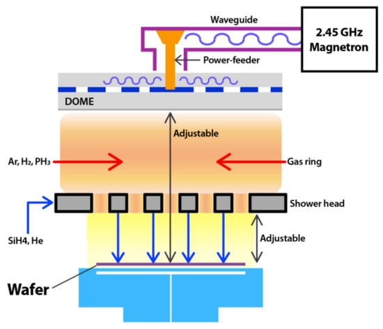
Figure 11.
Scheme of a MW-PECVD reactor used for the deposition of low-resistivity polycrystalline silicon. Reprinted from [54].
A remote-plasma reactor activated by microwaves (2.45 GHz) was used by Wrobek and coworkers [55] to achieve the deposition of hard a-SiCN coatings at a pressure of 75 Pa from a single silicon precursor mixed with hydrogen. Several precursor types were experimented with by the authors. Three belonged to the aminosilane family: (Dimethylamino)dimethylsilane (DMADMS), Bis(dimethylamino)methylsilane (BDMAMS), and Tris(dimethylamino)silane (TDMAS). The other two precursors belonged to the disilazane family: 1,1,3,3-Tetramethyldisilazane (TMDSN) and 1,3-Bis(dimethylsilyl)-2,2,4,4-tetramethylcyclodisilazane (BSCDSN). The scheme of the reactor is reprinted in Figure 12, in which a comparison is presented between a standard plasma reactor and a remote plasma device. In the former (Figure 12a), the plasma is generated in the same location where the substrate is positioned, providing the direct excitation of the deposition precursors. In the remote plasma reactor (Figure 12b), a non-precursor plasma, typically of H2, is produced in a region of the reactor that is physically separated by the sample holder, allowing the formation of highly reactive atomic hydrogen. A flow of plasma diffuses into the deposition region, where a filter removes charged particles, leaving only radicals to mix with the deposition precursors, giving rise to the dissociation process. The remote configuration is suitable for avoiding some effects such as ion bombardment on the growing film as well as excessive fragmentation of precursor molecules but increases the complexity of the reactor.
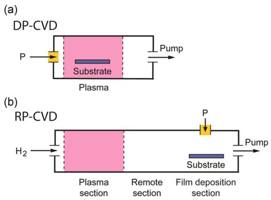
Figure 12.
A remote-plasma reactor activated by microwaves used for the deposition of hard a-SiCN coatings. (a) Standard plasma reactor; (b) remote plasma reactor. Reprinted from [55] with permission from John Wiley and Sons.
Microwave discharges were also investigated for the synthesis of nanostructures: Wollny and coworkers [56] employed a microwave-assisted PECVD reactor for the growth of silicon nanoparticles using a mixture of Ar, H2, and SiH4, directly injected into the plasma zone at a reduced pressure of 10 kPa. The silane precursor was dissociated in the plasma, giving rise to the production, by means of gas-phase nucleation, of nanoparticles that were transported by the plasma stream. The authors also developed a theoretical model to explain the synthesis process, employing a fluid dynamics model and a dispersed phase model.
A microwave-assisted technique was also used by Daoudi and coworkers [57] for the deposition by silane of silicon nanoparticles with diameter in range 7–37 nm. The microwaves were coupled with the precursors to form a flame-like plasma torch [58] that provided the silane dissociation followed by gas-phase nucleation. The produced nanoparticles were then decorated with silver nanoprisms which had been previously synthesized by chemical reduction from silver nitride.
A particular type of microwave-assisted plasma discharge is electron cyclotron resonance (ECR), in which the synergistic action of microwaves and a static magnetic field are used to achieve high electron energies. In this kind of discharge, the magnetic field intensity is tuned in such a way that the electron cyclotron frequency equals the microwave frequency, thus allowing resonant absorption of the microwave energy by the plasma electrons [59] (pp. 492–512.). In recent years, Miller and coworkers [60] reported an interesting study regarding the synthesis of terbium-doped silicon oxide (a-SiOx:Tb) by means of a novel hybrid deposition system, in which the silicon oxide was grown employing an ECR plasma of silane and oxygen while Tb atoms were generated by a magnetron sputtering source located in the same vacuum chamber. The authors achieved good control over the dopant incorporation in the films, being able to tune the Tb content in a range between 0.4–7.4 at.%.
2.5. Other Low Pressure Discharges
Apart from DC-, RF-, and MW-activated discharges, other types of discharges were also successfully used for the deposition of silicon-based materials, including gas jet and hollow electrode ones. The gas jet electron beam chemical vapor deposition (GJEB-CVD) technique [61] employs the formation of a supersonic jet of gas, which is then dissociated by a beam of high-energy electrons that crosses the gas flow, producing a flow of radicals that impinge directly on the substrate surface. Zamchiy and coworkers [62] employed this technique to achieve the synthesis of silicon oxide nanowires using a tin film as catalyst. In this work, a tin catalyst film 30 nm thick was first deposited by thermal evaporation and then heated to 400 °C and treated with a hydrogen plasma. The catalyst layer thus formed was then subjected to a high-speed flow of a gas mixture (silane plus argon and hydrogen), which was crossed by the electron beam to cause the ionization and dissociation of the precursor gas. Oxygen was injected into the reactor separately from the plasma stream. The process resulted in the formation of highly aligned SiOx nanowires.
The hollow electrode (anode or cathode) reactor employs the generation of a CCP discharge between two electrodes, one of which has at least a portion of itself shaped in the form of a cylinder, inside of which the gas flows. This particular electrode shape allows the formation of a more intense plasma with a higher electron density compared to a conventional parallel-plate CCP discharge. Tabuchi and coworkers [63] investigated the use of a hollow-anode PECVD reactor, the scheme of which is depicted in Figure 13, activated with a VHF-RF frequency of 105 MHz in an atmosphere of silane and hydrogen, to achieve the deposition of microcrystalline silicon at 300 °C. The system consisted of a VHF-powered cathode with a showerhead structure, by which the reactive gases were injected. A grounded anode was located parallel to the cathode at a distance of 13 mm (see Figure 13) in such a way that an empty space, called discharge space, was formed between the two electrodes. At the center of the anode surface, a small cylinder 10 mm in diameter was inserted, which completed the hollow electrode structure. The plasma was generated in the region between the two electrodes and, flowing through the cylinder, reached the deposition chamber, in which the plasma density was increased thanks to the electric field intensification. The authors investigated the effects of H2 dilution on the orientation of the crystals in the µc-Si films grown by this technique.
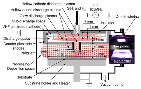
Figure 13.
Hollow anode VHF-PECVD reactor used for the deposition of microcrystalline silicon. Reprinted from [63] with permission from Elsevier.
2.6. Low Pressure Plasma Polymerization
Over many decades, plasma-polymerized organic thin films have been of great interest and, in particular, thin organosilicon films can be produced with different precursors/methodologies and aimed at a wide range of applications as multifunctional materials. Low-pressure plasma processes based on hexamethyldisiloxane (HDMSO) as a precursor were intensively studied since many years and widely reviewed only few years ago [64]. For this reason, hereinafter the solely most recent and peculiar advances will be reported. Kleines and coauthors obtained plasma-polymerized ultra-smooth SiOCH coatings deposited on polydimethylsiloxane (PDMS) substrates by MW (2.45 GHz) excitation in a PECVD reactor in order to acquire membranes [65] for the control of gas separation. According to process parameters (oxygen carrier-to-HDMSO monomer ratios and microwave power input), weaker cross-linking of the siloxane bonds as well as a more organic structure with an increased proportion of bound methyl groups was found advantageous for high permeability and separation performance in the coatings. Especially for the separation of He and N2, but also partly for other gas pairings (He/CO2 and CO2/N2), the selectivity for all test points decreased with increasing oxygen content in the process gas. Furthermore, the same authors explored the effect of energy density [66] on coated membrane permeation properties by varying MW power level as well as MW pulse duration. The highest permeation and separation performance of the produced layers was found in the low energy density range of the process, as the low power prevented strong fragmentation of the monomer, which resulted in less dense and cross-linked growth of the layers. Due to the low pulse durations, rearranging processes were suppressed and the layer structure did not become denser due to higher energy input. The conclusions were proven through several characterizations: ellipsometry, atomic force microscopy (AFM), X-ray photoelectron spectroscopy (XPS), Fourier transform infrared spectroscopy (FTIR), and field emission scanning electron microscopy (FESEM).
The HDMSO precursor was studied also for an opposite aim [67], i.e., to produce a SiOx-based barrier coating against atomic oxygen (AO) erosion when deposited on Kapton® (polyimide) by means of RF-activated plasma discharge by varying the ratio of O2/Ar in the reactor atmosphere, ranging from 50 to 1000 W in power. Kapton® is employed in the thermal blankets covering the external surface of spacecraft due to its thermo-optical properties and durability in harsh environments. When testing it in a coaxial ground-based AO simulation facility, it was found that in an AO fluence up to 1.09 × 10²² atoms/cm2, the uncoated sample was eroded and completely broken down. Conversely, when the coated polyimide film was under AO attack, the HDMSO-belonging methyl group were decomposed into volatile products (such as CO2, CO, and H2O), and the silicon formed a dense glassy SiOx layer resistant to further AO erosion.
HDMSO and hexamethyldisilazane (HDMSN) [68] were compared as precursors for SiOx-based O2 permeation barrier coatings and/or interlayers deposited on polyethylene terephthalate (PET) and polypropylene (PP) substrates by MW (2.45 GHz)-activated low pressure plasma polymerization. By means of mass spectrometry, the probability of dissociation of HMDSN at a given energy of incident electrons was higher than for HMDSO. Due to the higher number of smaller fragments, HDMSN coatings showed lower oxygen transmission rates (OTRs) for thicknesses greater than 2.5 nm (measured by ellipsometry) compared to HDMSO coatings. By increasing the content of oxygen in the process mixture, HDMSN seemed to produce highly cross-linked SiOx barrier coatings directly, adhering well to PP without the presence of the nanometric organic interlayer needed for PET.
The mechanism of organosilicon-based thin film deposition is still under investigation. Typically, the chemical interpretation mainly considers the recombination of free radicals, which is dominated by neutral radicals over ionic radicals. Thus, free radicals formed by the dissociation of precursor molecules diffuse to the surface of the film, where they are first physisorbed and migrate along the surface until they are desorbed or chemisorbed at a binding site on the film surface. A scheme of the possible mechanism is provided in Figure 14.
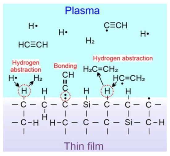
Figure 14.
Scheme of possible mechanism involved in HDMSO plasma polymerization. Reprinted from [69] with permission from John Wiley and Sons.
Recently, an interesting study of these fundamentals [69] was published, focusing on tetravinylsilane (TVS) and its plasma polymerization in a low-pressure PECVD reactor with the capacitively coupled discharge operated at 13.56 MHz in pulsed mode. The power dependence of the plasma species was examined with mass spectrometry. It was found that the deposition rate correlated with the flux of these species chemisorbed on the film surface if distinct sticking coefficients were taken into account. Then the carbon-to-silicon ratio in the deposited film strongly correlates with the C/Si flux ratio for the various power-controlled plasmas.
Considering other kinds of organosilicon precursors, tetraethoxysilane (TEOS) [70] was found to be a good candidate for using low pressure RF plasma polymerization to obtain an efficient thin film for increased biocompatibility of metal implants. The coating was deposited on sanded and nanotextured Ti6Al4V alloys, and surface and electrochemical properties and biological behavior were evaluated through the use of mesenchymal stem cells. If plasma polymerization techniques are used, this precursor for sol-gel-method SiO2 production can be employed to create thin film with more versatile properties, possibly including nanometric thickness.
Figure 15 shows that the samples sanded and polymerized by plasma have a higher number of viable stem cells than the surfaces nanotextured and polymerized by plasma.
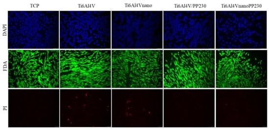
Figure 15.
Fluorescence microscopy with representative images of cell nuclei marked in blue (stained with DAPI), viable cells in green (stained with FDA), and non-viable cells in red (stained with PI) in the different experimental groups after 24 h of culture. Reprinted from [70] with permission from Elsevier.
For specific chemical functionalities, plasma polymerization, for instance, was applied to obtain nanometric organosilicon-based NH2-terminated films on silicon and aluminum samples by using (3-Aminopropyl)triethoxysilane (APTES) [71].
A pulsed and remote plasma (pulsed RP-PACVD), according to the experimental set-up in Figure 16, was used in order to produce a very soft plasma polymerization process and thus promote the growth of highly ordered organic coatings. The plasma was ignited in the discharge tube and the generated reactive species flowed out into a second reaction tube where the substrate holder was located, and the influence of the frequency, the duty cycle, ton and toff were investigated thoroughly. In addition to weight and spectroscopical characterizations, atmospheric pressure matrix-assisted light desorption ionization (MALDI) mass spectrometry was applied: oligomers containing up to eight APTES-derived monomers (C3H9NO2Si) and eight primary amine groups were undoubtedly detected and a density increase with the duration of toff was observed. Among these structures, silsesquioxanes (cages) which are uncommon as species obtainable by plasma processes, and cyclosiloxanes (rings) were clearly identified.
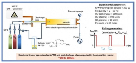
Figure 16.
Experimental setup. Reprinted from [71] with permission from John Wiley and Sons.
Fluorine-containing organosilicon monomers were widely used to tune the surface water adsorption/spreading/wetting for applications such as aerospace industry, self-cleaning, heat exchangers, power generation, low-friction coatings, anti-fogging properties or oil spill clean-up processes.
Section 2.2 reported a quite interesting example to obtain antifouling surfaces by means of the O2 RF plasma-activated functionalization by FOTS. Giner et al., instead, focused on the effects of FOTS grafted by means of a two-step chemical vapor deposition process (CVD) (the organosilane cross-linking, forming Si-O-Si surface bonds, was thermally promoted) onto a substrate coated with HDMSO plasma-polymerized films [72], that is, composed of flat SiOx. In fact, there is still the need to improve the analytical understanding of different states of adsorbed ultra-thin and extended water layers on nanorough substrates, both for macroscopically hydrophilic and hydrophobic surfaces. Thus, this kind of surface was compared to one consisting of SiOx microparticles deposited by water suspension and successively FOTS-functionalized, in order to explore the combined effect of chemistry and roughness on water adhesion behavior. The FOTS layer on the particles is more defect-rich than the one on the smooth PECVD SiOx film, and capillary bridges are formed at the contact points between the particles. Increased water adsorption is thus observed, notwithstanding the presence of the water-repulsive FOTS functionalization as depicted in Figure 17.
Figure 17.
Schematic representation (not to scale) of water adsorption at the spaces left by the FOTS cluster assembly (a). Capillary bridge formation takes place between asperities at the surface (b) and at the contact points between SiOx particles (c). Reprinted from [72] with permission from Elsevier.
Finally, researchers reported a double-step process composed of a hexamethyldisilazane (HMDSZ) plasma polymerization (PP) step and an acrylic acid (AA) grafting polymerization (GP) step to coat titanium (Ti) [73] and its alloys and zirconia (ZrO2) ceramics [74] in order to impart specific properties to materials used in dental implants applications. In the former case, first, a micro-arc oxidation (MAO) process, also called plasma electrolytic oxidation (PEO), was applied to Ti specimens in an electrolyte containing sodium silicate pentahydrate, potassium hydroxide, and ethylenediaminetetraacetic acid in distilled water, then a RF (13.56 MHz) LP plasma discharge in presence of HDMSZ vapours was activated to obtain a PP-SiOx coating and, lastly, an O2 plasma pre-treatment was carried out to form peroxide groups on the surface and thus facilitate UV light-induced AA GP by liquid immersion in the precursor of the pre-treated specimens, as shown in Figure 18.
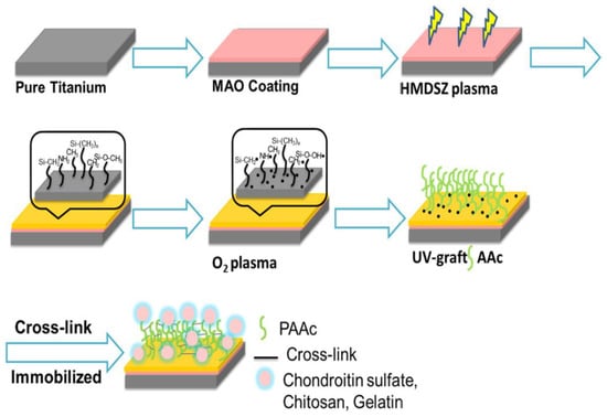
Figure 18.
The schematic illustration of the preparation of the functionalization of titanium surface modification. Reprinted from [73] with permission from Elsevier.
In the latter case, the zirconia ceramic surface was coated through RF-LP plasma discharge with the PP-SiOx, which was subsequently plasma-activated to promote the AA surface grafting. In both cases, the carboxylic terminations were used to immobilize biopolymers (chitosan, chitosan/poly g-glutamic acid, and gelatin) that enhance the materials’ biocompatibility and cell viability assays.
2.7. Resume of the Precursors Used at Low Pressure
In Table 1, a summary is given of the precursors used for low-pressure synthesis techniques of silicon-based materials that have been discussed in this section. Gases or vapors have not been included in the table if used only as dilution gases or dopants. As an example, nitrogen gas N2 was included if used to achieve nitrogen incorporation in the films, but not if it was used to dilute other precursor gases. Silane gas was by far the most used precursor gas and was employed for the synthesis of a wide range of materials, including all the phases of silicon, such as amorphous, nanocrystalline, or microcrystalline, but was also the most used gas for the synthesis of silicon-based nanostructures. Both ammonia and nitrogen were used for the synthesis of silicon-nitrogen and silicon-carbon-nitrogen alloys, while nitrous oxide was used in one case only, for the deposition of silicon-oxygen-nitrogen alloys. A considerable variety of gases and vapors were used to achieve the incorporation of carbon, ranging from methane to highly complex organic precursors. The latter, however, were mainly used to achieve the synthesis of silicon-carbon alloys through a single precursor. Diborane was used as a precursor (not as dopant gas) in one case only, to achieve the growth of silicon-boron-nitrogen alloys.

Table 1.
Precursors used for the plasma-assisted synthesis of Si-based materials at low pressure. For each precursor, the materials for the synthesis of which its use has been reported and the corresponding references are provided in the proper columns.
3. Synthesis by Means of Atmospheric Pressure Discharges
Atmospheric pressure plasma (APP) discharges allow the synthesis or the surface modification of materials while working at atmospheric pressure, thus avoiding the use of vacuum technology [75]. Interest in this kind of techniques has risen considerably in recent years, especially due to the lower cost and better applicability to inline industrial processes. While the first applications of APP techniques were mostly dedicated to the surface modification of textiles [76] and polymeric materials [77], the use of these processes for the synthesis of materials and nanostructures, including silicon-based ones, has increased considerably [78]. However, one of the main drawbacks of APP techniques is the requirement of much more intense power to achieve plasma formation compared with processes that work at low pressure. This sometimes makes this kind of technology less convenient from the point of view of reducing power consumption in industrial manufacturing due to environmental concerns. Moreover, in some APP techniques, such as plasma spray, a thermal plasma is produced with a very high-temperature plasma stream that can be detrimental to deposition on some kind of substrates that do not resist high temperatures. In the following, the most recent applications of APP techniques for the synthesis of silicon-based materials are reviewed, dividing the processes depending on the technique used for generating the atmospheric plasma. The last section has been dedicated specifically to the APP synthesis of Si-based polymeric materials.
3.1. Plasma Spray
Atmospheric plasma spray (APP) is a technique in which precursor powders are injected in a flow of plasma at atmospheric pressure, generated by means of a DC or RF discharge, and then transported to the substrate, where the adhesion process takes place to form a coating material. A similar technique was used by Wan and coworkers [79] to achieve the deposition of silicon nanospheres and nanosheets by injecting raw silicon powders into a flow of Ar plasma generated by a DC discharge at atmospheric pressure. A scheme of the deposition system is reprinted in Figure 19: the Ar flow was injected from the nozzle located on the top of the chamber and was excited in order to form the plasma stream by means of a DC power of 70 kW. The nanostructures were produced in the plasma by evaporation of the raw powders and subsequent gas phase nucleation and were collected on a plate positioned in the lower part of the reactor. More recently, Yang and coworkers [80] employed the injection of self-produced SiOx nanopowders with high silicon content into a flow of Ar plasma generated at atmospheric pressure using a RF-ICP excitation. The carrier gas was injected from the top part of the reactor and excited by a coil surrounding the cylindrical gas injector, powered by a 37 kW RF signal. The nanopowders were evaporated in the thermal-plasma stream and then re-nucleated. The process resulted in the deposition of SiOx nanowires with high silicon content, to be used in the production of high-performance lithium-ion battery anodes.
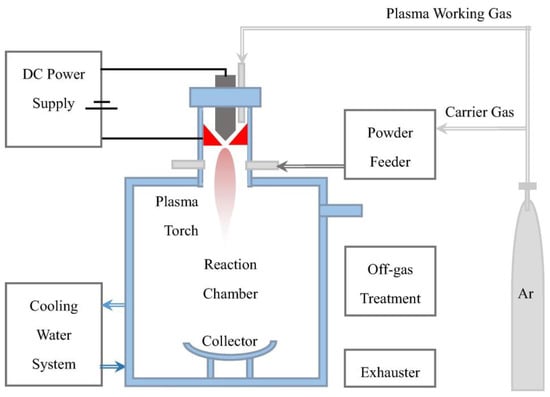
Figure 19.
Atmospheric pressure plasma spray system, used for the synthesis of silicon nanospheres and nanosheets. Reprinted from [79] with permission from Elsevier.
Zheng and coworkers [81] employed an APP plasma spray technique, using a power in a range between 40–44 kW, to achieve the deposition of nanostructured and conventional Yb2SiO5 coatings on SiC substrates, for application as environmental barrier coatings to prevent the oxidation of SiC-based turbines in aeromotive engines. The different film morphologies were achieved using different kinds of precursor powders to be injected into the plasma flow.
An APP technique was also used by Ma and coworkers [82] to achieve the formation of an Al-Si graded layer on the internal surface of cylindrical mechanical parts, such as pipe sections, made of aluminum, using a rotating plasma spraying gun, powered at about 45 kW, the scheme of which is reprinted in Figure 20, which could be inserted in the pipe cavity and was able to rotate while emitting the plasma flame, thus allowing the coating of the internal surfaces. The composition of the graded layer was changed during the deposition, starting with a pure SiAl layer and adding Cu and Fe in increasing quantities as the growth proceeded, with the aim of improving layer adhesion on the Al surface.
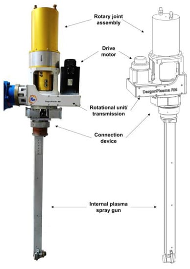
Figure 20.
Plasma reactor used for the deposition of Al-Si graded layers at atmospheric pressure on the internal surface of cylindrical mechanical parts. Reprinted from [82] with permission from Elsevier.
3.2. Plasma Jet
Plasma jet is a type of plasma technique, usually carried out at atmospheric pressure, in which a plasma discharge is activated in a reaction chamber, and a flow of plasma is then extracted from it and sent to a substrate, where it exerts its action of material growth or surface modification. Unlike plasma spray techniques, the precursors for the material growth are usually in the form of gases that are ionized and dissociated directly in the plasma stream. Moreover, this kind of technique usually uses a non-thermal plasma stream with a relatively low temperature.
Wang and coworkers [83] used an array of six plasma jet sources, the scheme of which is reprinted in Figure 21, to achieve the deposition of SiOx on a cylindrical aluminum surface. The plasma jet source was activated by a high-voltage AC power supply, using tetraethylorthosilicate (TEOS) as precursor and Ar as carrier gas [84]. Three non-adjacent coils were fed though channel 1 (see Figure 21) by means of Ar gas only and were used for etching, while the other three coils were fed through channel 2 with a mixture of TEOS and Ar and were used to provide the SiOx deposition. The plasma stream was excited using a dielectric barrier discharge structure [85].
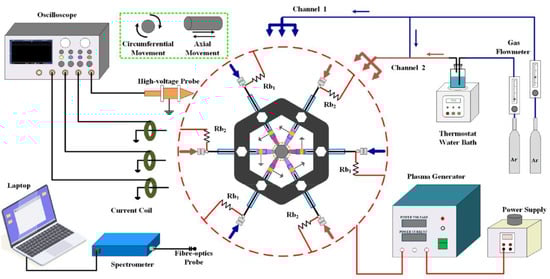
Figure 21.
Array of six plasma jet sources, used for the deposition of SiOx. Reprinted from [84] with permission from Elsevier.
A plasma jet surface treatment was also used by Xiong and coworkers [86] for the synthesis of nanocomposite coatings containing aluminum nitride (AlN) and methyltrimethoxysilane (MTMS). An Ar plasma jet, generated using a high-voltage power source at 10 kHz, was directed at the polyimide substrate, on which a mixture of AlN powders and MTMS had been previously deposited, transforming the two separate AlN and MTMS phases into nanostructured material formed of AlN nanoparticles embedded in a polymer matrix.
A novel type of plasma jet technique, called HelixJet, was recently employed by Dworschak and coworkers [87] for the synthesis of silicon nanocrystals (Si NC). The HelixJet plasma source employs an original electrode configuration, the scheme of which is reprinted in Figure 22, in which two metal electrodes are wired around a quartz tube, forming two spiral paths. One of the electrodes is grounded, while the other one is biased with a RF (13.56 MHz) at up to 250 W, giving rise to a synergistic action between the spiral-arranged electric field and the plasma filaments. Inside the plasma stream, the self-assembling of plasma filaments, which can rotate at considerable speeds, is achieved. The authors showed that, in such a configuration, the electric field lines produced inside the quartz tube match the orientation of the filaments, creating synergy between the spontaneous rotation and the external excitation. The system allowed the synthesis of SiOx particles of amorphous and crystalline structure as well as Si nanocrystals embedded in SiOx. Compared with other APP techniques such as the plasma spray, the HelixJet requires considerably less power, thus reducing its environmental impact.
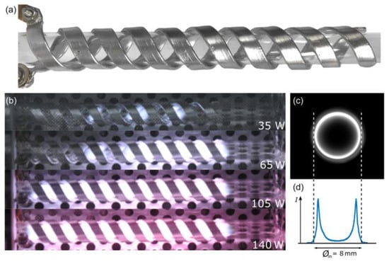
Figure 22.
Structure of the HelixJet reacto without plasma (a) and with He plasma at several powers (b). Front view taken with a telecentric lens (c) and corresponding intensity profile (d) of a plasma emission with 5 ppm silane concentration. Reprinted from [87] with permission from John Wiley and Sons.
3.3. Other APP Techniques
Apart from plasma spray and plasma jet, several other techniques can be used that work at atmospheric pressure, such as the corona discharge and the dielectric barrier discharge (DBD) methods, both of which are characterized by the formation of filamentary discharges produced by the accumulation of streamers [88]. Among the most interesting ones that were used recently for the growth of silicon-based materials, there is the technique used by Post and coworkers [89] for the synthesis of core-shell nanoparticles, employing a vapor-phase process at atmospheric pressure, in which the plasma generated in air by a DBD reactor was used to generate radicals that were then injected into a thermal reactor together with a previously generated nanoparticles aerosol and a tetraethyl orthosilicate (TEOS) or hexamethyldisiloxane (HMDSO) vapor flow. A scheme of the deposition process is reprinted in Figure 23: nanoparticles of Pt and Au were produced inside a spark generator, as shown in Figure 23a while TiO2 nanoparticles were atomized from an aqueous suspension, as can be seen in Figure 23b. All types of nanoparticles were coated using the reactive species produced inside a DBD plasma working at a power of 11 W. The nanoparticles were injected in spray form into a furnace, together with the output of the DBD reactor, inside which the coating process took place, giving rise to the core-shell structures, with the external layer composed of SiO2. It is noteworthy that the DBD plasma used in this process requires considerably low power.
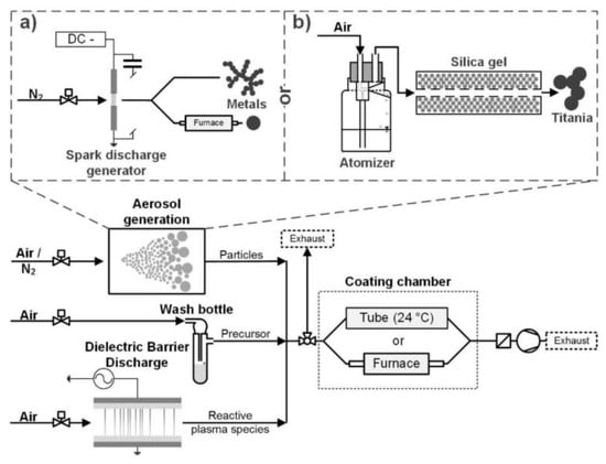
Figure 23.
Process flow used for the production of Au, Pt, or TiO2 nanoparticles, coated by SiO2 employing a DBD reactor. (a) Spark generator, used for Pt and Au nanoparticles generation; (b) atomizer, used for TiO2 nanoparticles production. Reprinted from [89].
Silicon-based materials were also synthesized employing APP-PECVD discharges, in which a uniform plasma, in contrast to filamentary discharges such as corona or DBD, is obtained at atmospheric pressure. Of particular interest are the results obtained by Kakiuchi and coworkers [90]. In that work, the deposition of a-Si thin films was achieved at low temperature and atmospheric pressure, using SiH4 as a precursor in a mixture of He and H2, employing a parallel-plate reactor with a VHF excitation at 150 MHz and a distance between the electrodes of 500 µm. The authors also investigated the effect of a pulsed discharge [91] in the same reactor and found that it provided a beneficial effect, allowing for the deposition of good quality a-Si films at a temperature as low as 120 °C. According to the data reported, the maximum power applied to the APP reactor was about 150 W, which is remarkably low compared to other techniques working at atmospheric pressure, allowing a reduced environmental impact.
3.4. Plasma Polymerization at Atmospheric Pressure
Plasma polymerization processes at atmospheric pressure (APP) have a large presence in industrial applications. Nowadays, HDMSO is still the most used monomer to produce a plethora of modifications of material surface properties, such as the reduction of the flammability of fir wood as well as control of its wettability [92], the superhydrophobicity of glass substrates [93], and the corrosion resistance [94] of steel specimens. The final thin film is, in all three cases, a SiOx coating with different chemical characteristics according to the desired function to be imparted and the type of atmospheric pressure plasma reactor and process conditions. A dielectric barrier discharge (DBD) apparatus, conceived for cotton textile processing, was used on fir wood [92] due to the ease of formation and production of a large-scale stable discharge. This process was carried out by using a carrier gas of pure argon containing monomer vapor flowing between two electrodes. Extensive characterization by means of FESEM, AFM, XPS, FTIR, EDX, and DTA-TG demonstrated the cross-linked nature of the macromolecular structures based on Si-C and PDMS-like Si-O-Si bonds, which clearly explains the water-repellent and fire-retardant nature of plasma-modified wood substrates.
Interestingly, for glass substrates coatings, an argon plasma jet at a relatively low-power frequency (11.5 kHz) was applied [93] with or without the use of several shielding gases, as depicted in Figure 24. XPS characterization demonstrated the different effects on chemical composition: N2 shielding preserved a high carbon content (in CH3 groups) from the precursor while minimizing the incorporation of oxygen into the coating surface.
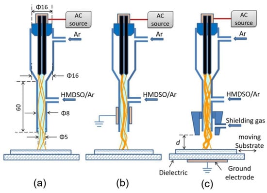
Figure 24.
Schematic diagram of plasma jet (a–c), reprinted from [93], with permission from Elsevier.
Moreover, it was found that O (from O and OH radicals) replaced C to form silica-like coating in cases where shielding gas was not present or with Ar and He shields. The plasma jet system used to treat the SAE 1020 steel surface [94] used a commercial AC power supply operated at 19.0 kHz to excite the discharge in an Ar/HDMSO atmosphere. Among the tested deposition modes (continuous or alternated), deposition time, and number of deposition steps, the most stable coatings, aiming for the formation of quartz-like inorganic material, were obtained with a three-step deposition and in both continuous and alternated modes.
A peculiar and very interesting organosilicon precursor, 2,4,6,8-tetramethylcyclotetrasiloxane (TMCTS), was chosen instead by Profili et al. [95] for the morphological and chemical modification of bleached, unrefined Kraft paper, that is, one of the by-products of woody biomass. The TMCTS precursor was selected for its ability to produce organosilicon coatings with relatively high deposition rates with respect to more conventional HDMSO. Plane-to-plane dielectric barrier discharges at atmospheric pressure were activated in the presence of the precursor (see the scheme depicted in Figure 25). It is worth noting that, during plasma processing of Kraft paper substrates, the amplitude of the applied voltage and its frequency were constantly adjusted to maintain a homogeneous discharge regime. In such conditions, the neutral gas temperature did not exceed 50 °C.
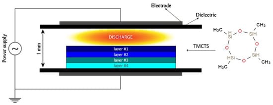
Figure 25.
Scheme of the DBD deposition system for TMCTS atmospheric plasma polymerization, reprinted from [95], with permission from Elsevier. Substrate layers formed of bleached unrefined Kraft paper are color-coded for clarity.
Finally, researchers observed a low plasma-assisted fragmentation of the TMCTS precursor and a partial oxidation of the TMCTS precursor fragments during the plasma deposition process. This mechanism led to the formation of a Si-O-Si network, thus imparting a high hydrophobicity to the coating and so improving the chemical and mechanical stability of cellulosic fabric subjected to humid environments.
3.5. Resume of the Precursors Used at Atmospheric Pressure
In Table 2, a summary is given of the precursors used for atmospheric-pressure synthesis techniques of silicon-based materials that have been discussed in this section. Gases or vapors have not been included in the table if used as transport gases in which precursors were injected in the solid form, as in the case of atmospheric-pressure plasma spray. A considerably lower number of precursors have been found compared with low-pressure techniques, which can be explained by two main considerations. On one hand, some of the most used APP techniques, such as plasma spray, do not rely on the dissociation of gaseous precursors to achieve the synthesis of materials but use a plasma discharge to achieve the formation of vapors from a solid source. On the other hand, working at atmospheric pressure imposes more limitations as to which gases and vapors can be used, both for safety considerations and due to the difficulty of preventing exposure to atmospheric gases.
Table 2.
Precursors used in the plasma-assisted synthesis of Si-based materials at atmospheric pressure. For each precursor, the materials for the synthesis of which its use has been reported and the corresponding reference are provided in the proper column.
Silane gas was used in the HelixJet and APP-PECVD techniques only. In both cases, the flow of gas, despite being at atmospheric pressure, was confined in a closed environment, as is necessary due to the extremely high reactivity of this gas with oxygen. In all the other works that have been reviewed, organic vapors were used if the synthesis was achieved through gas dissociation.
4. Conclusions
In this work, we have reviewed the most important improvements in the synthesis of silicon-based materials by means of plasma-assisted techniques that have been published in recent years. A wide range of techniques have been included, ranging from classical RF-PECVD and sputtering to more innovative and exotic techniques, and several types of silicon-based thin films, both inorganic and organic, as well as nanostructures of different types and shapes, have been described. The results confirm that plasma-assisted techniques constitute a very versatile and powerful collection of methods for the synthesis of silicon-based materials, and new and innovative techniques have been developed in recent years that promise important developments in silicon-based technology.
Low-pressure CCP techniques, which have a longer history among the plasma-assisted synthesis processes, are still of great importance. In fact, these processes were originally designed for the synthesis of amorphous, nanocrystalline, and microcrystalline materials, but are now widely used for the synthesis of several types of nanostructures, such as nanospheres and nanowires. A considerable amount of research has also been devoted to improving the passivation properties of amorphous silicon and silicon oxide films used in heterojunction solar cells, which are very promising for the aim of increasing the efficiency of energy production from renewable sources. Interesting improvements have also been made in CCP reactor design, e.g., allowing for the deposition of patterned thin films, with a high potential for reducing the need for high-cost lithographic processes. Several improvements have been achieved for other types of low-pressure processes also, such as ICP and MW techniques, which have been especially used for the dissociation of high strongly bonded precursors, such as N2, or to achieve the deposition of complex compounds, as well as to allow the deposition of good quality thin films at low temperatures.
Atmospheric pressure techniques have a shorter history compared to low-pressure ones, but the use of these processes has considerably increased in recent years due to their high potential for reducing the cost of silicon-based materials synthesis in several industrial applications. Techniques such as plasma spray and plasma jet, which have been in use for a considerable amount of time, are still widely used, but the former is highly power demanding compared to other techniques. HelixJet and APP-PECVD are the most innovative among the reviewed APP techniques and show the advantage of high versatility and low power consumption. In fact, the further development of these techniques could lead to very interesting innovations in the synthesis of silicon-based materials.
In perspective, increased use of APP techniques can be expected in the next years as new methods are developed and existing ones improved, reducing typical drawbacks, such as the nonuniformity of filamentary discharges or the high power consumption of thermal plasmas. In fact, atmospheric pressure techniques have a high potential to reduce the production cost of silicon-based material synthesis in several application fields, such as large-area electronics, sensor development, and the biomedical field.
On the other hand, reduced pressure techniques are continually evolving and the development of new specialized processes can be expected in the coming years. Of special interest are hybrid techniques, which mix more than one type of plasma excitation source in order to achieve more effective dissociation of reactive gases. Localized growth techniques, which allow for the patterned deposition of thin films, thus reducing the need of lithographic processes, are also expected to be improved in the near future. Another field in which important developments are expected is the reduction of process temperatures, increasing the number of silicon-based materials that can be grown on polymeric substrates and improving the quality of these materials.
Author Contributions
All authors contributed to conceptualization, methodology, investigation, writing—original draft preparation, writing—review and editing. P.M. contributed to the review of inorganic materials synthesis techniques; P.R. contributed to the review of plasma-polymerization processes. All authors have read and agreed to the published version of the manuscript.
Funding
This research received no external funding.
Institutional Review Board Statement
Not applicable.
Informed Consent Statement
Not applicable.
Data Availability Statement
Not applicable.
Conflicts of Interest
The authors declare no conflict of interest.
References
- Tayaba, S.; Sethi, H.; Shahid, H.; Malik, R.; Ikram, M.; Ali, S.; Khaliq, S.; Khan, Q.; Maqbool, M. Silicon-Germanium and carbon-based superconductors for electronic, industrial, and medical applications. Mater. Sci. Eng. B 2023, 290, 116332. [Google Scholar] [CrossRef]
- Ballif, C.; Haug, F.-J.; Boccard, M.; Verlinden, P.J.; Hahn, G. Status and perspectives of crystalline silicon photovoltaics in research and industry. Nat. Rev. Mater. 2022, 7, 597–616. [Google Scholar] [CrossRef]
- Mussano, F.; Genova, T.; Laurenti, M.; Munaron, L.; Pirri, C.F.; Rivolo, P.; Carossa, S.; Mandracci, P. Hydrogenated amorphous silicon coatings may modulate gingival cell response. Appl. Surf. Sci. 2018, 436, 603–612. [Google Scholar] [CrossRef]
- Mandracci, P.; Mussano, F.; Ceruti, P.; Pirri, C.F.; Carossa, S. Reduction of bacterial adhesion on dental composite resins by silicon–oxygen thin film coatings. Biomed. Mater. 2015, 10, 015017. [Google Scholar] [CrossRef] [PubMed]
- Osminkina, L.A.; Agafilushkina, S.N.; Kropotkina, E.A.; Saushkin, N.Y.; Bozhev, I.V.; Abramchuk, S.S.; Samsonova, J.V.; Gambaryan, A.S. Antiviral adsorption activity of porous silicon nanoparticles against different pathogenic human viruses. Bioact. Mater. 2022, 7, 39–46. [Google Scholar] [CrossRef] [PubMed]
- Guo, H.; Cao, S.; Li, L.; Zhang, X. A review on the mainstream through-silicon via etching methods. Mater. Sci. Semicond. Process. 2022, 137, 106182. [Google Scholar] [CrossRef]
- Daghbouj, N.; Cherkashin, N.; Darras, F.-X.; Paillard, V.; Fnaiech, M.; Claverie, A. Effect of the order of He+ and H+ ion co-implantation on damage generation and thermal evolution of complexes, platelets, and blisters in silicon. J. Appl. Phys. 2016, 119, 135308. [Google Scholar] [CrossRef]
- Cherkashin, N.; Daghbouj, N.; Seine, G.; Claverie, A. Impact of He and H relative depth distributions on the result of sequential He+ and H+ ion implantation and annealing in silicon J. Appl. Phys. 2018, 123, 161556. [Google Scholar] [CrossRef]
- Daghbouj, N.; Li, B.S.; Callisti, M.; Sen, H.S.; Karlik, M.; Polcar, T. Microstructural evolution of helium-irradiated 6H–SiC subjected to different irradiation conditions and annealing temperatures: A multiple characterization study. Acta Mater. 2019, 181, 160–172. [Google Scholar] [CrossRef]
- Martinu, L.; Zabeida, O.; Klemberg-Sapieha, J.E. Plasma-Enhanced Chemical Vapor Deposition of Functional Coatings. In Handbook of Deposition Technologies for Films and Coatings, 3rd ed.; Martin, P.M., Ed.; Elsevier: Oxford, UK, 2010; pp. 392–465. [Google Scholar]
- Vasudev, M.C.; Anderson, K.D.; Bunning, T.J.; Tsukruk, V.V.; Naik, R.R. Exploration of plasma-enhanced chemical vapor deposition as a method for thin-film fabrication with biological applications. ACS Appl. Mater. Interfaces 2013, 5, 3983–3994. [Google Scholar] [CrossRef] [PubMed]
- Huff, M. Recent advances in reactive ion etching and applications of high-aspect-ratio microfabrication. Micromachines 2021, 12, 991. [Google Scholar] [CrossRef] [PubMed]
- Chabert, P.; Tsankov, T.V.; Czarnetzki, U. Foundations of capacitive and inductive radio-frequency discharges. Plasma Sources Sci. Technol. 2021, 30, 024001. [Google Scholar] [CrossRef]
- Delfani-Abbariki, S.; Abdollah-zadeh, A.; Hadavi, S.M.M.; Abedi, M.; Derakhshandeh, S.M.R. Enhancing the adhesion of diamond-like carbon films to steel substrates using silicon-containing interlayers. Surf. Coat. Technol. 2018, 10, 1436–1440. [Google Scholar] [CrossRef]
- Lakhonchai, A.; Chingsungnoen, A.; Poolcharuansin, P.; Chanlek, N.; Tunmee, S.; Rittihong, U. Improvement of corrosion resistance and mechanical properties of chrome plating by diamond-like carbon coating with different silicon-based interlayers. Mater. Res. Express 2022, 9, 055604. [Google Scholar] [CrossRef]
- Sun, S.; Wu, Y.; Wang, Z.; Zhang, Y.; Chen, D.; Chen, J. Plasma enabled in-situ deposition of hybrid structured SiOx/C on polymorphous carbon hosts for superior lithium storage. Carbon 2023, 205, 253–261. [Google Scholar] [CrossRef]
- Grenadyorov, A.S.; Solovyev, A.S.; Oskomov, K.V.; Sypchenko, V.S. Influence of deposition conditions on mechanical properties of a-C:H:SiOx films prepared by plasma-assisted chemical vapor deposition method. Surf. Coat. Technol. 2018, 349, 547–555. [Google Scholar] [CrossRef]
- Grenadyorov, A.S.; Solovyev, A.A.; Oskomov, K.V.; Semenov, V.A.; Zhulkov, M.O.; Sirota, D.A.; Chernyavskiy, A.M.; Karmadonova, N.A.; Malashchenko, V.V.; Litvinova, L.S.; et al. Morphofunctional reaction of leukocytes and platelets in in vitro contact with a-C:H:SiOx-coated Ti–6Al–4V substrate. J. Biomed. Mater. Res. Part A 2023, 111, 309–321. [Google Scholar] [CrossRef] [PubMed]
- Ohta, R.; Fukada, K.; Tashiro, T.; Dougakiuchi, M.; Kambara, M. Effect of PS-PVD production throughput on Si nanoparticles for negative electrode of lithium ion batteries. J. Phys. D 2018, 51, 105501. [Google Scholar] [CrossRef]
- Harder, B.J. Oxidation performance of Si-HfO2 environmental barrier coating bond coats deposited via plasma spray-physical vapor deposition. Surf. Coat. Technol. 2020, 384, 125311. [Google Scholar] [CrossRef]
- Mandracci, P.; Gazia, R.; Virga, A. New Research on the Plasma-Assisted Deposition Of Silicon-Based Amorphous Thin Film Alloys. In Amorphous Materials: New Research, 1st ed.; Mishra, S.B., Ed.; Nova Science Pub Inc.: New York, NY, USA, 2013; pp. 27–50. [Google Scholar]
- Mandracci, P.; Ricciardi, C. Silicon-carbon-oxynitrides grown by plasma-enhanced chemical vapor deposition technique. Thin Solid Film. 2007, 505, 7639–7642. [Google Scholar] [CrossRef]
- Ruan, T.; Qu, M.; Wang, J.; He, Y.; Xu, X.; Yu, C.; Zhang, Y.; Yan, H. Effect of deposition temperature of a-Si:H layer on the performance of silicon heterojunction solar cell. J. Mater. Sci. Mater. Electron. 2019, 30, 13330–13335. [Google Scholar] [CrossRef]
- Özkol, E.; Procel, P.; Zhao, Y.; Mazzarella, L.; Medlin, R.; Šutta, P.; Isabella, O.; Zeman, M. Effective Passivation of Black Silicon Surfaces via Plasma-Enhanced Chemical Vapor Deposition Grown Conformal Hydrogenated Amorphous Silicon Layer. Phys. Status Solidi-Rapid Res. Lett. 2020, 14, 1900087. [Google Scholar] [CrossRef]
- Sai, H.; Hsu, H.-J.; Chen, P.-W.; Chen, P.-L.; Matsui, T. Intrinsic Amorphous Silicon Bilayers for Effective Surface Passivation in Silicon Heterojunction Solar Cells: A Comparative Study of Interfacial Layers. Phys. Status Solidi A 2021, 218, 2000743. [Google Scholar] [CrossRef]
- Wang, J.; Ru, X.; Ruan, T.; Hu, Y.; Zhang, Y.; Yan, H. Performance of heterojunction solar cells with different intrinsic a-Si:H thin layers deposited by RF- and VHF-PECVD. J. Mater. Sci. Mater. Electron. 2021, 32, 25327–25331. [Google Scholar] [CrossRef]
- Pandey, A.; Bhattacharya, S.; Panigrahi, J.; Mandal, S.; Komarala, V.K. Effect of Gas Flow Rate in PECVD of Amorphous Silicon Thin Films for Interface Passivation of Silicon Heterojunction Solar Cells. Phys. Status Solidi A 2022, 219, 2200183. [Google Scholar] [CrossRef]
- Ouaras, K.; Filonovich, S.; Bruneau, B.; Wang, J.; Ghosh, M.; Johnson, E. Maskless interdigitated a-Si:H PECVD process on full M0 c-Si wafer: Homogeneity and passivation assessment. Sol. Energy Mater. Sol. Cells 2022, 246, 111927. [Google Scholar] [CrossRef]
- Chen, W.; Truong, T.N.; Nguyen, H.T.; Samundsett, C.; Pheng Phang, S.; MacDonald, D.; Cuevas, A.; Zhou, L.; Wan, Y.; Yan, D. Influence of PECVD deposition temperature on phosphorus doped poly-silicon passivating contacts. Sol. Energy Mater. Sol. Cells 2020, 206, 110348. [Google Scholar] [CrossRef]
- Truong, T.N.; Yan, D.; Nguyen, C.T.; Kho, T.; Guthrey, H.; Seidel, J.; Al-Jassim, M.; Cuevas, A.; Macdonald, D.; Nguyen, H.T. Morphology, microstructure, and doping behaviour: A comparison between different deposition methods for poly-Si/SiOx passivating contacts. Prog. Photovolt. Res. Appl. 2021, 29, 857–868. [Google Scholar] [CrossRef]
- Wang, Y.; Liu, H.; Shen, W. A Convenient and Effective Method to Deposit Low-Defect-Density nc-Si:H Thin Film by PECVD. Nanoscale Res. Lett. 2018, 13, 234. [Google Scholar] [CrossRef] [PubMed]
- Sharma, M.; Chaudhary, D.; Sudhakar, S.; Kumar, S. Intrinsic Sub-Nanocrystalline Silicon Thin Films: Active Layer for Solar Cells. Silicon 2021, 13, 1–7. [Google Scholar] [CrossRef]
- Wang, S.-H.; Chang, H.-E.; Lee, C.-C.; Fuh, Y.-K.; Li, T.T. Evolution of a-Si:H to nc-Si:H transition of hydrogenated silicon films deposited by trichlorosilane using principle component analysis of optical emission spectroscopy. Mater. Chem. Phys. 2020, 240, 122186. [Google Scholar] [CrossRef]
- Ghosh, H.; Mitra, S.; Siddiqui, M.S.; Saxena, A.K.; Chaudhuri, P.; Saha, H.; Banerjee, C. Back scattering involving embedded silicon nitride (SiN) nanoparticles for c-Si solar cells. Opt. Commun. 2018, 413, 63–72. [Google Scholar] [CrossRef]
- Chen, J.; Li, D.; Sun, T.; Han, J.; Zhang, Y.; Li, W.; Xu, J.; Chen, K. Experimental observations on metal-like carrier transport and Mott hopping conduction behaviours in boron-doped Si nanocrystal multilayers. Nanotechnology 2023, 34, 16LT01. [Google Scholar] [CrossRef] [PubMed]
- Shibata, K.; Kato, S.; Kurosawa, M.; Gotoh, K.; Miyamoto, S.; Usami, N.; Kurokawa, Y. Preparation and thermoelectric characterization of boron-doped Si nanocrystals/silicon oxide multilayers. Jpn. J. Appl. Phys. 2023, 62, SC1074. [Google Scholar] [CrossRef]
- Li, X.; Jin, R.; Li, L.; Lu, J.; Gu, Y.; Ren, F.; Huang, J. Effect of deposition rate on the growth mechanism of microcrystalline silicon thin films using very high frequency PECVD. Optik 2019, 180, 104–112. [Google Scholar] [CrossRef]
- Liu, J.; Zhang, Y.; Fan, Z.; Sun, H.; Shan, F. Low-temperature deposition of large-grain polycrystalline Si thin films on polyethylene terephthalate. Thin Solid Film. 2020, 707, 138065. [Google Scholar] [CrossRef]
- Song, J.; Huang, R.; Zhang, Y.; Lin, Z.; Zhang, W.; Li, H.; Song, C.; Guo, Y.; Lin, Z. Effect of Nitrogen Doping on the Photoluminescence of Amorphous Silicon Oxycarbide Films. Micromachines 2019, 10, 649. [Google Scholar] [CrossRef]
- Hang, L.; Liu, W.; Xu, J.; Yang, C.; Zhou, S. Effects of various substrate materials on microstructural and optical properties of amorphous silicon oxynitride thin films deposited by plasma-enhanced chemical vapor deposition. Thin Solid Film. 2020, 709, 138186. [Google Scholar] [CrossRef]
- Ke, W.; Yang, K.; Zhu, X.D. Investigation on formation of thin Si-B-N films on stainless steel by plasma chemical vapor deposition. Appl. Surf. Sci. 2021, 565, 150583. [Google Scholar] [CrossRef]
- Wang, W.; Ngo, E.; Florea, I.; Foldyna, M.; Roca i Cabarrocas, P.; Maurice, J.-L. Room Temperature Growth of Silica Nanowires on Top of Ultrathin Si Nanowires Synthesized with Sn-Cu Bimetallic Seeds. Phys. Status Solidi A 2021, 218, 2100409. [Google Scholar] [CrossRef]
- Azrak, E.; Xue, Z.; Liu, S.; Chen, W.; Castro, C.; Duguay, S.; Pareige, P.; Yu, L.; Roca i Cabarrocas, P. Ultrahigh Incorporation of Tin in SiSn Nanowires Grown via In-Plane Solid-Liquid-Solid Mechanism. Appl. Surf. Sci. 2023, 618, 156637. [Google Scholar] [CrossRef]
- Baranov, A.I.; Morozov, I.A.; Uvarov, A.V.; Gudovskikh, A.S. Capacitance characterization of GaP/Si superlattice grown by time-modulated PECVD. J. Phys. Conf. Ser. 2019, 1410, 012116. [Google Scholar] [CrossRef]
- Uvarov, A.V.; Gudovskikh, A.S.; Baranov, A.I.; Maksimova, A.A.; Kudryashov, D.A.; Vyacheslavova, E.A.; Yakovlev, G.E.; Zubkov, V.I. Plasma-Deposited Multilayer GaP/Si p-i-n Structure for Tandem Silicon-Based Solar Cells. ACS Appl. Energy Mater. 2021, 5, 5374–5380. [Google Scholar] [CrossRef]
- Zhang, H.; Zhang, W.; Su, R.; Tu, H.; Shi, L.; Hu, J. Deuterium trapping in the carbon-silicon co-deposition layers prepared by RF sputtering in D2 atmosphere. J. Nucl. Mater. 2018, 501, 217–223. [Google Scholar] [CrossRef]
- Neßlinger, V.; Welzel, S.; Rieker, F.; Meinderink, D.; Nieken, U.; Grundmeier, G. Thin Organic-Inorganic Anti-Fouling Hybrid-Films for Microreactor Components. Macromol. React. Eng. 2023, 17, 2200043. [Google Scholar] [CrossRef]
- Mostofi Sarkari, N.; Doğan, Ö.; Bat, E.; Mohseni, M.; Ebrahimi, M. Assessing effects of (3-aminopropyl)trimethoxysilane self-assembled layers on surface characteristics of organosilane-grafted moisture-crosslinked polyethylene substrate: A comparative study between chemical vapor deposition and plasma-facilitated in situ grafting methods. Appl. Surf. Sci. 2019, 497, 143751. [Google Scholar]
- Rumyantsev, Y.M.; Chagin, M.N.; Shayapov, V.R.; Yushina, I.V.; Kichai, V.N.; Kosinova, M.L. Synthesis and Properties of Thin Films Formed by Vapor Deposition from Tetramethylsilane in a Radio-Frequency Inductively Coupled Plasma Discharge. Glass Phys. Chem. 2018, 44, 174–182. [Google Scholar] [CrossRef]
- Yang, K.; De Sagazan, O.; Pichon, L.; Salaün, A.-C.; Coulon, N. Inductively Coupled Plasma Chemical Vapor Deposition for Silicon-Based Technology Compatible with Low-Temperature (≤220 °C) Flexible Substrates. Phys. Status Solidi A 2020, 217, 1900556. [Google Scholar] [CrossRef]
- Song, H.; Seo, S.; Chang, H. Study on SiN and SiCN film production using PE-ALD process with high-density multi-ICP source at low temperature. Curr. Appl. Phys. 2018, 18, 1436–1440. [Google Scholar] [CrossRef]
- Jung, C.; Song, S.; Lee, N.; Kim, Y.; Lee, E.J.; Lee, S.G.; Jeon, H. Characteristics of Silicon Oxide Thin Film Deposited via Remote Plasma Atomic Layer Deposition. ECS J. Solid State Sci. Technol. 2021, 10, 043005. [Google Scholar] [CrossRef]
- Takenaka, K.; Setsuhara, Y.; Han, J.G.; Uchida, G.; Ebe, A. Plasma-enhanced reactive linear sputtering source for formation of silicon-based thin films. Rev. Sci. Instrum. 2018, 89, 083902. [Google Scholar] [CrossRef] [PubMed]
- Kim, Y.; Lee, M.; Kim, Y.-J. Selective Growth and Contact Gap-Fill of Low Resistivity Si via Microwave Plasma-Enhanced CVD. Micromachines 2019, 10, 689. [Google Scholar] [CrossRef] [PubMed]
- Wrobel, A.M.; Uznanski, P. Hard silicon carbonitride thin-film coatings produced by remote hydrogen plasma chemical vapor deposition using aminosilane and silazane precursors. 1: Deposition mechanism, chemical structure, and surface morphology. Plasma Process. Polym. 2021, 18, 2000240. [Google Scholar] [CrossRef]
- Wollny, P.; Menser, J.; Engelmann, L.; Sellmann, J.; Schulz, C.; Wiggers, H.; Kempf, A.; Wlokas, I. The role of phase transition by nucleation, condensation, and evaporation for the synthesis of silicon nanoparticles in a microwave plasma reactor—Simulation and experiment. Chem. Eng. J. 2023, 453, 139695. [Google Scholar] [CrossRef]
- Daoudi, K.; Columbus, S.; Falcão, B.P.; Pereira, R.N.; Peripolli, S.B.; Ramachandran, K.; Hadj Kacem, H.; Allagui, A.; Gaidi, M. Label-free DNA detection using silver nanoprism decorated silicon nanoparticles: Effect of silicon nanoparticle size and doping levels. Spectrochim. Acta A 2023, 290, 122262. [Google Scholar] [CrossRef]
- Knipping, J.; Wiggers, H.; Rellinghaus, B.; Roth, P.; Konjhodzic, D.; Meier, C. Synthesis of High Purity Silicon Nanoparticles in a Low Pressure Microwave Reactor. J. Nanosci. Nanotechnol. 2004, 4, 1039–1044. [Google Scholar] [CrossRef] [PubMed]
- Lieberman, M.A.; Lichtemberg, A.J. Principles of Plasma Discharges and Materials Processing, 2nd ed.; John Wiley & Sons, Inc.: Hoboken, NJ, USA, 2005. [Google Scholar]
- Miller, J.W.; Khatami, Z.; Wojcik, J.; Bradley, J.D.B.; Mascher, P. Integrated ECR-PECVD and magnetron sputtering system for rare-earth-doped Si-based materials. Surf. Coat. Technol. 2018, 336, 99–105. [Google Scholar] [CrossRef]
- Baranov, E.A.; Khmel, S.Y.; Zamchiy, A.O. Synthesis of amorphous silicon films with high growth rate by gas-jet electron beam plasma chemical vapor deposition method. IEEE Trans. Plasma Sci. 2014, 42, 2794. [Google Scholar] [CrossRef]
- Zamchiy, A.O.; Baranov, E.A.; Khmel, S.Y. Tin-catalyzed oriented array of microropes of silicon oxide nanowires synthesized on different substrates. Vacuum 2018, 147, 99–106. [Google Scholar] [CrossRef]
- Tabuchi, T.; Toyoshima, Y.; Fujimoto, S.; Takashiri, M. Optimized hydrogen concentration within a remotely induced hollow-anode plasma for fast chemical-vapor-deposition of photosensitive and <110>-preferential microcrystalline silicon thin-films. Thin Sol Film. 2020, 694, 137714. [Google Scholar]
- De Freitas, A.S.M.; Maciel, C.C.; Rodrigues, J.S.; Ribeiro, R.P.; Delgado-Silva, A.O.; Rangel, E.C. Organosilicon films deposited in low-pressure plasma from hexamethyldisiloxane—A review. Vacuum 2021, 19, 110556. [Google Scholar] [CrossRef]
- Kleines, L.; Wilski, S.; Alizadeh, P.; Rubner, J.; Wessling, M.; Hopmann, C.; Dahlmann, R. Evaluation of the membrane performance of ultra-smooth silicon organic coatings depending on the process energy density. Thin Solid Film. 2022, 748, 139169. [Google Scholar] [CrossRef]
- Kleines, L.; Wilski, S.; Alizadeh, P.; Rubner, J.; Wessling, M.; Hopmann, C.; Dahlmann, R. Structure and gas separation properties of ultra-smooth PE-CVD silicon organic coated composite membranes. Surf. Coat. Technol. 2021, 42, 127338. [Google Scholar] [CrossRef]
- Mu, H.; Wang, X.; Li, Z.; Xie, Y.; Gao, Y.; Liu, H. Preparation and atomic oxygen erosion resistance of SiOx coating formed on polyimide film by plasma polymer deposition. Vacuum 2019, 165, 7–11. [Google Scholar] [CrossRef]
- Mitschker, F.; Schücke, L.; Hoppe, C.; Jaritz, M.; Dahlmann, R.; De Los Arcos, T.; Hopmann, C.; Grundmeier, G.; Awakowicz, P. Comparative study on the deposition of silicon oxide permeation barrier coatings for polymers using hexamethyldisilazane (HMDSN) and hexamethyldisiloxane (HMDSO). J. Phys. D Appl. Phys. 2018, 51, 235201. [Google Scholar] [CrossRef]
- Cech, V.; Branecky, M. Nonthermal tetravinylsilane plasma used for thin-film deposition: Plasma chemistry controls thin-film chemistry. Plasma Process. Polym. 2022, 19, 2100192. [Google Scholar] [CrossRef]
- Pereira, M.; Baldin, E.K.; Antonini, L.M.; Bernardi, F.; Oliveira, L.; Maurmann, N.; Pranke, P.; Pereira, M.B.; Malfatti, C. de F. TEOS thin films obtained by plasma polymerization on Ti6Al4V alloys: Influence of the deposition pressure on surface properties and cellular response. Appl. Surf. Sci. Adv. 2021, 5, 100123. [Google Scholar] [CrossRef]
- Bulou, S.; Lecoq, E.; Loyer, F.; Frache, G.; Fouquet, T.; Gueye, M.; Belmonte, T.; Choquet, P. Study of a pulsed post-discharge plasma deposition process of APTES: Synthesis of highly organic pp-APTES thin films with NH 2 functionalized polysilsesquioxane evidences. Plasma Process. Polym. 2019, 16, 1800177. [Google Scholar] [CrossRef]
- Giner, I.; Torun, B.; Han, Y.; Duderija, B.; Meinderink, D.; Orive, A.G.; de los Arcos, T.; Weinberger, C.; Tiemann, M.; Schmid, H.J.; et al. Water adsorption and capillary bridge formation on silica micro-particle layers modified with perfluorinated organosilane monolayers. Appl. Surf. Sci. 2019, 475, 873–879. [Google Scholar] [CrossRef]
- Liao, S.C.; Chang, C.T.; Chen, C.Y.; Lee, C.H.; Lin, W.L. Functionalization of pure titanium MAO coatings by surface modifications for biomedical applications. Surf. Coat. Technol. 2020, 394, 125812. [Google Scholar] [CrossRef]
- Ho, K.N.; Chen, L.W.; Kuo, T.F.; Chen, K.S.; Lee, S.Y.; Wang, S.F. Surface modification of zirconia ceramics through cold plasma treatment and the graft polymerization of biomolecules. J. Dent. Sci. 2023, 18, 73–80. [Google Scholar] [CrossRef]
- Tendero, C.; Tixier, C.; Tristant, P.; Desmaison, J.; Leprince, P. Atmospheric pressure plasmas: A review. Spectrochim. Acta B 2006, 61, 2–30. [Google Scholar] [CrossRef]
- Teli, M.D.; Pandit, P.; Samanta, K.K. Application of atmospheric pressure plasma technology on textile. J. Text. Assoc. 2015, 75, 422–428. [Google Scholar]
- Baniya, H.B.; Guragain, R.P.; Subedi, D.P. Cold atmospheric pressure plasma technology for modifying polymers to enhance adhesion: A critical review. Prog. Adhes. Adhes. 2021, 6, 841–880. [Google Scholar]
- Mariotti, D.; Sankaran, R.M. Perspectives on atmospheric-pressure plasmas for nanofabrication J. Phys. D 2011, 44, 174023. [Google Scholar] [CrossRef]
- Wan, X.; Chen, X.; Yang, S.; Ma, W.; Li, S.; Wei, K. Facile synthesis of silicon nanospheres and nanosheets using DC thermal plasma. Mater. Lett. 2020, 268, 127616. [Google Scholar] [CrossRef]
- Yang, Z.; Dong, Y.; Liu, C.; Feng, X.; Jin, H.; Ma, X.; Ding, F.; Li, B.; Bai, L.; Ouyang, Y.; et al. Design and synthesis of high-silicon silicon suboxide nanowires by radio-frequency thermal plasma for high-performance lithium-ion battery anodes. Appl. Surf. Sci. 2023, 614, 156235. [Google Scholar] [CrossRef]
- Zheng, T.; Xu, B.; Wang, S.; Guo, D.; Zhou, F.; Wang, Y.; Fang, D. Microstructure and nanomechanical properties of plasma-sprayed nanostructured Yb2SiO5 environmental barrier coatings. J. Am. Ceram. Soc. 2023, 106, 2666–2678. [Google Scholar] [CrossRef]
- Ma, G.-Z.; He, P.-F.; Wang, H.-D.; Tian, H.-G.; Zhou, L.; Yong, Q.-S.; Liu, M.; Zhao, H.-C.; He, D.-Y. Promoting bonding strength between internal Al-Si based gradient coating and aluminum alloy cylinder bore by forming homo-epitaxial growth interface. Mater. Des. 2023, 227, 111764. [Google Scholar] [CrossRef]
- Wang, R.; Xia, Z.; Kong, X.; Liang, L.; Ostrikov, K. Etching and annealing treatment to improve the plasma-deposited SiOx film adhesion force. Surf. Coat. Technol. 2021, 427, 127840. [Google Scholar] [CrossRef]
- Wang, R.; Xia, Z.; Kong, X.; Xue, S.; Wang, H. Uniform deposition of silicon oxide film on cylindrical substrate by radially arranged plasma jet array. Surf. Coat. Technol. 2022, 437, 128365. [Google Scholar] [CrossRef]
- Wang, R.; Liu, Y.; Xue, S.; Xie, P.; Yang, W. Substrate temperature induced structure transformation in plasma film deposition process. Surf. Coat. Technol. 2022, 451, 129071. [Google Scholar] [CrossRef]
- Xiong, C.; Wang, Y.; Lin, L.; Gao, M.; Huang, Y.; Chu, P.K. Deposition of nanocomposites coating on polyimide films by atmospheric pressure plasma for enhanced thermal conductivity. Surf. Interfaces 2023, 37, 102758. [Google Scholar] [CrossRef]
- Dworschak, M.; Kohlmann, N.; Matějka, F.; Galář, P.; Kienle, L.; Schäfer, J.; Benedikt, J. Silicon nanocrystal synthesis with the atmospheric plasma source HelixJet. Plasma Process. Polym. 2023, 20, 2200129. [Google Scholar] [CrossRef]
- Nijdam, S.; Teunissen, J.; Ebert, U. The physics of streamer discharge phenomena. Plasma Sources Sci. Technol. 2020, 29, 103001. [Google Scholar] [CrossRef]
- Post, P.; Wurlitzer, L.; Maus-Friedrichs, W.; Weber, A.P. Characterization and Applications of Nanoparticles Modified in-Flight with Silica or Silica-Organic Coatings. Nanomaterials 2018, 8, 530. [Google Scholar] [CrossRef] [PubMed]
- Kakiuchi, H.; Ohmi, H.; Yasutake, K. Controllability of structural and electrical properties of silicon films grown in atmospheric-pressure very high-frequency plasma. J. Phys. D 2018, 51, 355203. [Google Scholar] [CrossRef]
- Kakiuchi, H.; Ohmi, H.; Yasutake, K. Pulsed very high-frequency plasma-enhanced chemical vapor deposition of silicon films for low-temperature (120 °C) thin film transistors. J. Phys. D 2020, 53, 15201. [Google Scholar] [CrossRef]
- Sohbatzadeh, F.; Shabannejad, A.; Ghasemi, M.; Mahmoudsani, Z. Deposition of halogen-free flame retardant and water-repellent coatings on firwood surfaces using the new version of DBD. Prog. Org. Coat. 2021, 151, 106070. [Google Scholar] [CrossRef]
- Trinh, Q.H.; Nguyen, D.B.; Hossain, M.M.; Mok, Y.S. Deposition of superhydrophobic coatings on glass substrates from hexamethyldisiloxane using a kHz-powered plasma jet. Surf. Coat. Technol. 2019, 361, 377–385. [Google Scholar] [CrossRef]
- Silva, L.L.G.; Kodaira, F.V.P.; Fagundes, P.V.M.; Quade, A.; Kostov, K.G. Study of Organosilicon Films Deposited on SAE 1020 Steel by Atmospheric Plasma Jet for Corrosion Protection. Braz. J. Phys. 2022, 5, 114. [Google Scholar] [CrossRef]
- Profili, J.; Asadollahi, S.; Vinchon, P.; Dorris, A.; Beck, S.; Sarkassian, A.; Stafford, L. Recent progress on organosilicon coatings deposited on bleached unrefined Kraft paper by non-thermal plasma process at atmospheric pressure. Prog. Org. Coat. 2020, 147, 105865. [Google Scholar] [CrossRef]


Disclaimer/Publisher’s Note: The statements, opinions and data contained in all publications are solely those of the individual author(s) and contributor(s) and not of MDPI and/or the editor(s). MDPI and/or the editor(s) disclaim responsibility for any injury to people or property resulting from any ideas, methods, instructions or products referred to in the content. |
© 2023 by the authors. Licensee MDPI, Basel, Switzerland. This article is an open access article distributed under the terms and conditions of the Creative Commons Attribution (CC BY) license (https://creativecommons.org/licenses/by/4.0/).