Abstract
An electrowetting display (EWD) is a new reflective display device with the advantages of paper display, high reflectivity, and fast response times. However, the display performance of EWDs has been restricted by oil film splitting and luminance oscillation. Therefore, a new driving waveform based on a falling slope function and a high-voltage, square-wave reset signal is proposed to solve these defects. It consists of a shrinkage stage and a stabilizing stage. First, the oil film of a pixel can be quickly ruptured by applying a falling slope function during the shrinkage stage according to the oil film-splitting theory. Then, a direct current (DC) voltage is applied to promote the complete fusion of the dispersed oil films by analyzing the voltage characteristic curves of EWDs. Finally, a high-voltage, square-wave reset signal is applied during the stabilizing stage to reduce luminance oscillations and suppress oil film backflow. Experimental results show that the average luminance was increased by 6.5% compared with a PWM driving waveform. The display stability of EWDs was improved by 89.1% compared with a driving waveform with a rising gradient.
1. Introduction
Electrowetting (EW) is a phenomenon that changes the wettability of an insulating layer’s material surface via the application of an external electric field, and it causes displacement and the deformation of droplets [1]. Its theory was first proposed in 1981, and it has been widely used in the biomedical, chemical, and display fields [2,3,4,5]. In 2003, Hayes et al. proposed the concept of an electrowetting display (EWD) based on electrowetting and microfluidic technology [6]. Compared with the traditional electrophoresis display technology, it has the advantages of a fast response time, readability in a robust light environment, and video playback [7,8,9,10,11]. However, EWDs have some defects, such as low luminance due to oil film splitting and a low display stability affected by luminance oscillation [12,13,14]. Therefore, it is essential to improve the display performance of EWDs by optimizing the driving scheme to suppress oil film splitting effectively.
Pixels are the main component of EWDs, and the switching process of a pixel is driven by an applied electric field [15,16]. The electric field sequence is called a driving waveform. The oil film’s motion state and contraction degree can be controlled by applying different driving waveforms, ultimately affecting the stability of pixels in EWDs [17,18,19]. However, there is oil film splitting, oil film backflow, luminance oscillation, and long response times when EWDs are driven by the traditional PWM driving waveform [20,21,22,23]. Hence, a new driving waveform was proposed to solve the oil film-splitting phenomenon in EWDs [24]. The new driving waveform increased the driving voltage from its threshold to its maximum voltage by establishing a power function model, which effectively suppressed oil film splitting caused by voltage mutation. However, the response time of EWDs increased, and a high frame rate display could not be maintained. Then, an optimized driving waveform was proposed based on an overdriving voltage [25]. The overdriving voltage was introduced to shorten the response time in the oil film-splitting stage, and a DC driving voltage was applied to obtain the target luminance in the driving stage. However, it could not improve the charge-trapping problem in the insulating layer. Therefore, a dynamic adaptive display driving waveform based on a thin film transistor-electrowetting display (TFT-EWD) was proposed to solve the discontinuous static image display defect caused by charge capture [26]. The driving waveform used the DC hybrid driving model and the source non-polarized model (SNPM). It could efficiently maintain the stable display of static and dynamic images. At the same time, it could also improve reflection luminance. In addition, a multi-DC overspeed driving waveform was proposed to resolve the inconsistency of grayscale images caused by oil film backflow [27]. The driving waveform consisted of a start-up driving stage and a stable driving stage. A square-wave signal with an adjustable duty cycle and frequency was introduced in the start-up driving stage to complete the grayscale image display. Then, an overspeed pulse was introduced in the stable driving stage to reduce the average voltage difference during high and low voltage conversion. This driving scheme could effectively improve grayscale consistency. These driving schemes related to the optimization of EWD performance have provided a new design idea for subsequent research.
This paper proposes a new combined pulse-driving waveform using the electrowetting principle and the oil film-splitting theory. In order to reduce oil film splitting during the oil shrinkage stage, relationships among the falling slope, driving time, and luminance of pixels were studied. Then, oil film was fully shrunk using a DC driving voltage to obtain the saturation luminance of EWDs. Finally, a square waveform reset signal was used to reduce luminance oscillation and release trapped charges, which improved the display stability of EWDs.
2. Principle of EWDs
2.1. Principle of EWDs
The basic structure of an EWD pixel is similar to a stack. It is formed by stacking a top plate on top of pixel walls, two indium tin oxide (ITO) electrodes, a glass substrate, polar liquid (NaCl liquid), colored oil film, and a hydrophobic insulating layer (fluoropolymer) [28,29,30], as shown in Figure 1. Of these layers, only the color of the oil film and the substrate can be displayed through pixels; it is essentially an optical switch with superior grayscale display characteristics [12]. When an electric field is not applied between the electrodes, the colored oil film stably covers the insulating layer’s surface and forms a film. At this time, it is in an “off” state. When a certain electric field is applied between the electrodes, the stable state of the oil film in the pixel is broken, and the oil film ruptures and shrinks to the corners of the pixel via the action of the electric field force [31]. At this time, it is in an “on” state.
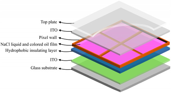
Figure 1.
A spatial schematic diagram of the typical pixel structure of EWDs. It comprises a glass substrate, two ITO electrodes, a hydrophobic insulating layer, NaCl liquid, colored oil film, pixel walls, and a top plate.
In addition, the contact angle of the oil film is related to the driving voltage between the two ITO electrodes in EWDs. A change in the contact angle can affect the aperture ratio and luminance display of EWDs. The correspondence between the contact angle of oil film and the driving voltage can be described by the classical Lippmann–Young equation, as shown in Equation (1) [32]:
where and are the dynamic and static contact angles of the oil film, respectively, is the height of the insulating layer, is the oil–liquid interfacial tension, is the dielectric constant in a vacuum, and is the dielectric constant of the insulating layer. is the voltage value of the applied electric field. , and are determined by the nature and temperature of the material itself. In addition, it can be seen from Equation (1) that the changing trends of the contact angle and the driving voltage are positively correlated. However, as a result of oil film splitting and charge trapping, part of the charges may be trapped in the insulating layer during the driving process. This creates a reverse electric field between the electrodes, thereby weakening the original electric field and affecting the stable display of EWDs. Therefore, it is necessary to revise the Lippmann–Young equation to remedy this defect [33]:
where is the voltage amplitude of the reverse electric field. The modified Lippmann–Young equation can more accurately describe the relationship between contact angles and driving voltages.
2.2. Oil Film Splitting
Oil film splitting refers to the rupture of an oil film when the driving voltage between ITO electrodes exceeds the threshold voltage for oil film rupture. At this time, the oil film quickly shrinks to two or more corners of a pixel and cannot be recombined, as shown in Figure 2. In addition, the threshold voltage of oil film rupture can be derived from Equation (3) [34]:
where is the threshold voltage of the oil film, is the unit length of the pixel in EWDs, and and are the height and the dielectric constant of the oil film, respectively. It can be seen that the threshold voltage of oil film rupture is related to the dielectric constant, oil film height, pixel size, and other factors [35]. The degree of oil film rupture depends on the applied driving voltage. When the driving voltage is lower than the threshold voltage, oil film will not rupture, and the luminance of the pixel remains unchanged. When the driving voltage exceeds the threshold voltage, the oil film ruptures at its thinnest part. The ruptured oil film shrinks along the pixel wall, and the surface area of the shrunken oil film can be calculated using Equation (4) [36]:
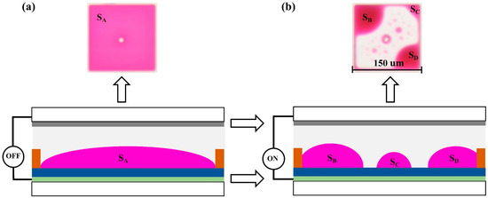
Figure 2.
The phenomenon of oil film splitting in pixels. (a) When no driving voltage is applied, the insulating layer is stably covered with a complete oil film. is the surface area when oil film is tiled. (b) When the driving voltage is applied, the oil film splits into three parts under the action of an electric field and shrinks to different corners. , , and represent the surface area of the split oil film shrunk to different corners.
It can be found that when the oil film in a pixel is split into multiple oil films, the exposed area of the substrate gradually decreases. It affects the luminance display of EWDs and reduces the aperture ratio. Therefore, effectively solving oil film splitting is an important research direction for improving the performance of EWDs.
3. Experimental Results and Discussion
3.1. Experimental Platform
In this experiment, the performance of EWDs was characterized by measuring luminance–time data. The oscillation range of a pixel’s saturation luminance could characterize the stability of the pixel, and the change rate of its luminance–time curve could reflect its response speed. Therefore, we assembled a set of experimental equipment for the luminance measurement of EWDs. It included a function generator, a voltage amplifier, a computer, a colorimeter, and an electron microscope, as shown in Figure 3. Table 1 shows the specific parameters of these devices. The specific practical steps were as follows.
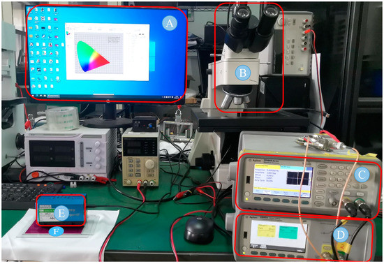
Figure 3.
The experimental platform for testing the oil film-splitting phenomenon in EWDs. (A) A computer. It completed the complication and output of the driving waveform. (B) An electron microscope. It was used to observe the shrinkage state of the oil film in pixels. (C) A function generator. It was used to output a specific driving waveform to drive the EWD. (D) A voltage amplifier. It completed amplitude amplification of the driving waveform to achieve the output of the target voltage. (E) A colorimeter. It was used to collect luminance changes in the EWD. (F) An EWD.

Table 1.
Parameters of equipment used in this experiment.
First, the Matlab software was used on the computer to compile the driving waveform and output the waveform file in text format. Then, the output waveform file was converted into the corresponding format using the Arbexpress software and stored in a Universal Serial Bus (USB). Meanwhile, the waveform file was imported into the function generator through the USB. Because the voltage output range of the function generator in the experiment equipment was positive or negative 5 V, it could not meet the driving conditions of EWDs. Therefore, the amplitude of the waveform signal was amplified by 10 using the voltage amplifier. Finally, a colorimeter was placed on EWDs to measure their luminance, and the motion state of the oil film in the pixel was observed with an electron microscope. The structural parameters of EWDs are shown in Table 2.
Table 2.
Parameters of the EWDs used in this experiment.
3.2. Proposed Driving Waveforms
In order to solve the defects of low display stability and luminance oscillation caused by oil film splitting, a combined waveform with multistage driving was designed in this study. It can be divided into shrinkage and stabilizing stages, as shown in Figure 4.
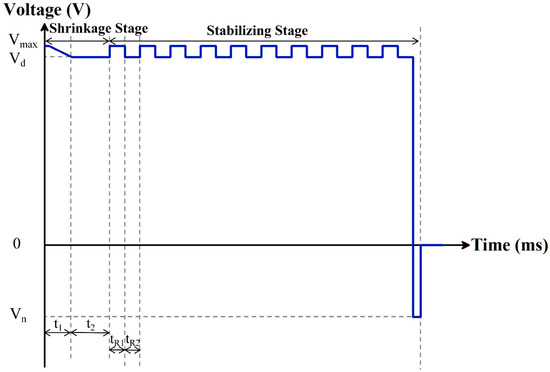
Figure 4.
A schematic diagram of the proposed driving waveform for suppressing oil film splitting. It consists of a shrinkage stage and a stabilizing stage. The shrinkage stage comprises a falling slope function and a DC voltage; the stabilizing stage comprises a high-voltage, square-wave signal and a reset signal. is the maximum driving voltage of the EWD pixel, is the driving voltage of the target grayscale, is the negative voltage of the reset signal. and are the durations of the falling slope function and the DC voltage, respectively. and are the durations of the high and low voltages, respectively, of the high-voltage, square-wave signal.
In the shrinkage stage, a falling slope function model was introduced. The driving voltage declined from the maximum voltage to the driving voltage of a target grayscale at a specific slope. The oil film ruptured quickly because of the high driving voltage, and the response speed of the EWDs was significantly improved. The model of the falling slope function is shown in Equation (5):
where is the driving voltage corresponding to the duration of , is the falling slope, and is the duration of the applied driving voltage. The falling slope was controlled by adjusting the driving voltage of the target grayscale to achieve the best suppression effect. At the end of the shrinkage stage, the DC voltage was used to drive oil film in the horizontal direction. It caused the ruptured oil film to fully converge and fuse, suppressing oil film splitting. However, the number of trapped charges in the insulating layer increased with the driving time. This weakened the control that the external electric field had on the movement of the oil film. In order to improve the performance of EWDs, a reset signal was used to release the trapped charges in a timely manner, thereby strengthening the external electric field’s control of the oil film. Therefore, this driving waveform released the trapped charges using a high-voltage, square-wave signal with an adjustable duty cycle and a reset signal of several milliseconds, thus effectively suppressing the charge-trapping effect.
3.3. Testing of the Shrinkage Stage
In our experiment, the voltage characteristic curve of the EWDs was measured first, as shown in Figure 5. By applying DC voltages to the EWDs, the luminance data were observed using the colorimeter. It could be seen that the luminance of the EWDs was almost unchanged when the DC voltage was less than 12 V, indicating that the oil film was stably covered on the insulating layer. When the DC voltage was higher than 12 V, the luminance of the EWDs changed suddenly, indicating that the oil film had ruptured. Therefore, the threshold voltage of the EWDs was set to 12 V. In addition, the voltage characteristic curve of the EWDs shows an upward trend. When the DC voltage exceeded 30 V, the voltage characteristic curve gradually tended to become more stable. In order to reduce power consumption and prevent irreversible damage to the EWDs caused by an excessive DC voltage, the maximum driven voltage of the EWDs was set to 35 V.
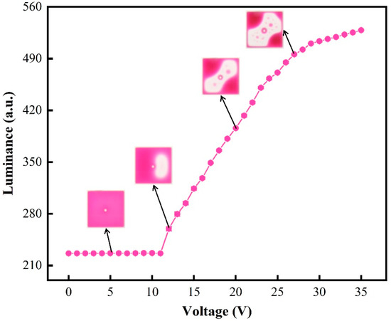
Figure 5.
The voltage characteristic curve of an EWD. The measuring range of DC voltage was 0–35 V. The oil film began to rupture when the DC voltage was 12 V.
In the shrinkage stage, the effects of falling slope and driving time on the EWD’s luminance was studied to suppress oil film splitting. The falling slope was set to 5–30 mV/ms, and was set to 10–50 ms. The luminance variation trend of the EWDs was driven by different and falling slopes, as shown in Figure 6. It can be seen that the saturation luminance of the EWDs decreased gradually with an increase in the falling slope and . The luminance of the EWDs was the lowest when the falling slope and were 30 mV/ms and 50 ms, respectively. This is because the driving voltage significantly decreased when the EWDs were driven for a long time with a high falling slope. As a result, the EWDs could not maintain high luminance. In addition, the saturation luminance of the EWDs was the largest when the falling slope was 10 mV/ms and was 10 ms. Therefore, the falling slope and were set to 10 mV/ms and 10 ms, respectively.
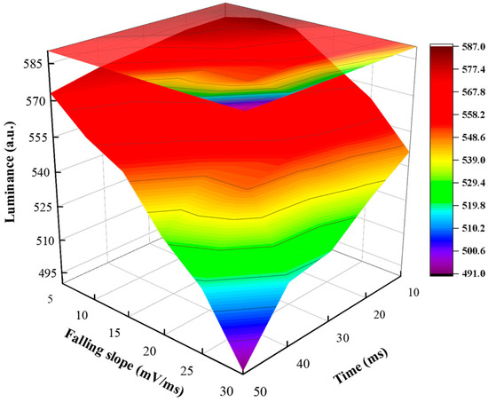
Figure 6.
A three-dimensional image of the relationship between the luminance of EWDs and falling slopes and s. The maximum luminance of the EWDs was 587 when the falling slope was 10 mV/ms and was 10 ms.
However, the ruptured oil film could not be fully shrunk into the corners of the pixel using only the falling slope function. Therefore, a DC driving signal was introduced in the shrinkage stage. Because of influences from response time that must be considered, the driving time of the DC signal should not be set too long. In this experiment, the range of was set to 0–100 ms, and its luminance change state is shown in Figure 7. It can be seen that, when was less than 60 ms, the luminance curve of the EWDs shows an upward trend. It shows that the shrinkage degree of the oil film increased gradually. On the contrary, the luminance of the EWDs started to decline when exceeded 60 ms. This is because a long driving time led to oil film backflow, thus reducing the display luminance of the EWDs. To sum up, the EWDs had the best performance when was 60 ms.
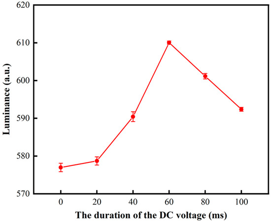
Figure 7.
The luminance curve of the EWDs was driven by the DC voltage. Within 0–60 ms, the luminance curve shows an upward trend. Within 60–100 ms, the luminance gradually decreased from the peak value, and the luminance curve shows a downward trend. When was set to 60 ms, EWDs had the best performance.
3.4. Testing of the Stabilizing Stage
In the stabilizing stage, the influence of different negative voltages on the EWD’s luminance was measured, as shown in Figure 8. Additionally, a comparison of the driving effects is listed in Table 3. Through experimental measurement, it was determined that the and of the square-wave signal were 35 V and 34 V, respectively. The experimental results show that the average luminance value was low, and there was apparent luminance oscillation when the negative voltage was less than −25 V. However, with an increase in the negative voltage, the luminance curve of the EWDs gradually rose. This is because the reset signal was not high enough to fully released the trapped charges when the negative voltage was low. When the negative voltage was gradually increased, the number of released charges increased and the reverse electric field was weakened, so the luminance value of the EWDs was effectively improved. The average luminance value of the EWDs was 656 when the negative voltage was −35 V. Additionally, the standard deviation of the luminance value was the smallest. That was, the display state of the EWDs was relatively stable and oil film backflow could be suppressed. Therefore, the negative voltage of the reset signal was selected as −35 V.
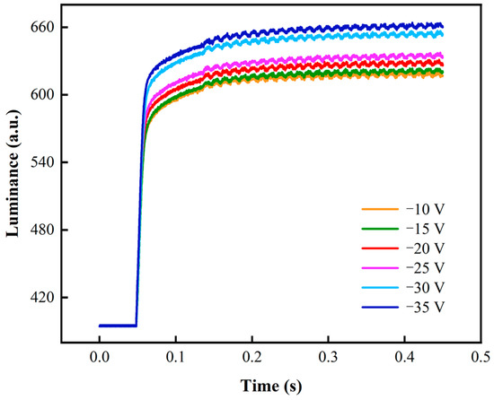
Figure 8.
The luminance–time curve corresponds to different negative voltages for the reset signal. The average luminance of EWDs increased with an increase in negative voltage. The average luminance was 656 when the negative voltage was −35 V.
Table 3.
Driving effect when EWDs were driven by different negative voltages in the reset signal.
In addition, the display stability of the EWDs was seriously affected by luminance oscillation during the driving process. Therefore, it was necessary to set the duty ratio of the high-voltage, square-wave signal reasonably to suppress luminance oscillation. The duty ratio was defined as the ratio between and . In this experiment, five groups of duty ratios were selected for comparison. They were 1:4, 2:3, 1:1, 3:2, and 4:1. Their luminance curves are shown in Figure 9, and the driving results are listed in Table 4. It can be seen that there was obvious luminance oscillation in the pixel, and the average luminance value of the EWDs was low when the duty ratio of the square-wave signal was lower than 3:2. This is because the duration of the high-voltage signal was short, and oil film recombination was insufficient, resulting in the appearance of luminance oscillation during the process of high and low level conversion. Therefore, there were luminance differences when the EWDs displayed the same grayscale. With an increased duty ratio in the square-wave signal, the luminance–time curve gradually became smooth, and the EWDs could reach saturation luminance. When the duty ratio was 3:2, the average luminance of the EWDs was 658, and luminance oscillation could not be observed on the EWD panel. However, the average luminance of the EWDs decreased and the luminance curve oscillated slightly when the duty ratio exceeded 3:2. Therefore, the duty ratio of the high-voltage, square-wave signal was set to 3:2.
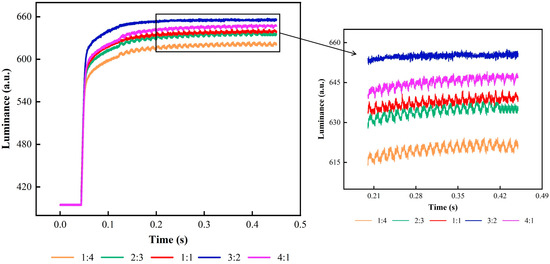
Figure 9.
The luminance–time curve when EWDs were driven by a high-voltage, square-wave signal with different duty ratios. The luminance curve’s oscillation degree decreased with the increase in duty ratio. When the duty ratio of the square-wave signal was 3:2, the luminance curve tended to be stable without apparent luminance oscillation.
Table 4.
Driving effect comparison when different duty ratios were used in the high-voltage, square-wave signal to drive the EWDs.
3.5. Performance of the Proposed Waveform
In order to test the suppression effect of the proposed driving waveform on oil film splitting, two different driving waveforms were selected for performance comparison, as shown in Figure 10A. The two driving waveforms being compared were the PWM driving waveform [25] and a driving waveform with a rising gradient [35]. In order to ensure consistency in the parameters, the high and low levels of the PWM driving waveform were set to 35 V and 0 V, respectively. At the same time, the driving waveform with a rising gradient retained its optimal parameters. In addition, the driving period of the two comparison waveforms was consistent with the proposed driving waveform.
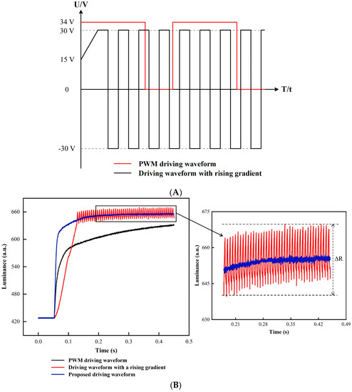
Figure 10.
The structure diagram and performance comparison of three different driving waveforms. (A) The structure diagram of two comparison waveforms. The red line represents the PWM driving waveform. The black line represents the driving waveform with a rising gradient. (B) The luminance–time curve of three driving waveforms within 0.5 s. The PWM driving waveform’s luminance curve rose with an increase in driving time and could not reach saturation luminance. The driving waveform with a rising gradient produced a certain amplitude of luminance oscillation, and the amplitude was 29.7. However, the EWD could achieve a stable luminance using the proposed driving waveform.
Figure 10B shows the luminance curve of the EWDs using three different driving waveforms. Additionally, the driving effect is shown in Table 5. By analyzing the luminance rising curve, it was found that the response time of the PWM driving waveform was the shortest at only 63 ms. On the contrary, the response times of the proposed driving waveform and the driving waveform with a rising gradient were 97 ms and 127 ms, respectively. It is because the high-voltage driving time was longer and could break the steady state of the oil film more quickly. However, the high voltage caused oil film splitting. Therefore, the average luminance of the PWM driving waveform was only 614, and the luminance curve changed with an increased driving time, so it could not maintain stability. However, the proposed driving waveform trended gradually toward stability when the luminance rose to 645. The luminance curve did not produce luminance oscillation. On the contrary, the driving waveform with a rising gradient produced luminance oscillation with an amplitude of , and apparent flickers could be observed on the EWDs. The experimental results show that the average luminance of the proposed driving waveform was 654, and the standard deviation was 0.68. The standard deviation of the driving waveform with a rising gradient was 6.23. The average luminance of the EWDs was improved by 6.5% compared with the PWM driving waveform, and its stability was increased by 89.1% compared with the driving waveform with a rising gradient.
Table 5.
Comparison of driving effects when different driving waveforms were used to drive EWDs.
In order to visually identify the experimental effects, state diagrams of the oil film driven by three different driving waveforms are shown in Figure 11. When the PWM driving waveform drove the EWDs, it can be seen that there was an apparent oil film-splitting phenomenon in the pixel, and split oil films could not be reorganized. Oil film splitting could be effectively suppressed when the EWDs was driven by the other two driving waveforms. However, there were some small, dispersed oil films in the pixel when the EWDs were driven by the driving waveform with a rising gradient. This reduced the luminance of the EWDs. Hence, the proposed driving waveform obtained the largest luminance values.
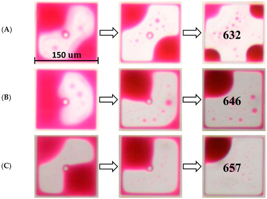
Figure 11.
Different driving waveforms drove the state of oil film in pixels. (A) The pixel was driven by the PWM driving waveform. The maximum luminance was 632. (B) The pixel was driven by the driving waveform with a rising gradient. The maximum luminance was 646. (C) The pixel was driven by the proposed driving waveform. The maximum luminance was 657.
4. Conclusions
In this paper, a combined driving waveform comprising the falling slope function and a high-voltage, square-wave reset signal was proposed based on the driving principle of EWDs and the theory of oil film splitting, aiming to reduce the effects of oil film splitting and luminance oscillation in EWDs. During the driving process, the falling slope function was applied to rupture the oil film rapidly, and the split oil film was then fused again by applying DC voltage. In addition, trapped charges were released on time by applying a high-voltage, square-wave reset signal to prevent luminance oscillation and oil film backflow. Compared with two conventional driving waveforms, the average luminance of the proposed driving waveform could reach 654, and the standard deviation of luminance remained at 0.68. Therefore, applying the proposed driving waveform could significantly improve the saturation luminance and display stability of EWDs, which could provide a certain research direction for the design of driving waveforms and the performance optimization of EWDs.
Author Contributions
Z.L. designed this project and conducted most experiments and data analysis. Z.Y. performed part of the experiments and helped with discussions during manuscript preparation. Z.Y., J.W. and L.L. revised the paper. F.C., L.S., D.T. and H.W. gave suggestions on project management and provided helpful discussions on the experimental results. All authors have read and agreed to the published version of the manuscript.
Funding
This research was funded by the National Natural Science Foundation of China (no.62105056), the Special Projects in Key Fields of Regular Colleges and Universities in Guang-dong Province (no. 2022ZDZX1046), the Engineering Technology Research Center of Colleges and Universities in Guang-dong Province (no. 2021GCZX005), and the Innovation Team of Colleges and Universities in Guang-dong Province (no. 2021KCXTD040).
Data Availability Statement
Data are contained within the article.
Conflicts of Interest
The authors declare no conflict of interest.
References
- Jones, T. An Electromechanical interpretation of electrowetting. J. Micromechan. Microeng. 2005, 15, 1184–1187. [Google Scholar] [CrossRef]
- Beni, G.; Hackwood, S. Electrowetting displays. Appl. Phys. Lett. 1981, 38, 207–209. [Google Scholar] [CrossRef]
- Sethi, S.; Kadian, S.; Gogoi, R.; Manik, G. Layer-by-layer fabrication of self-cleaning superhydrophobic surface made from Carboxymethylcellulose and ZnO quantum dots: A combined experimental and computational study. Surf. Interfaces 2023, 37, 102752. [Google Scholar] [CrossRef]
- Sethi, S.; Singh, M.; Manik, G. A multi-scale modeling and simulation study to investigate the effect of roughness of a surface on its self-cleaning performance. Mol. Syst. Des. Eng. 2020, 5, 1277–1289. [Google Scholar] [CrossRef]
- Zhang, S.; Huang, J.; Chen, Z.; Lai, Y. Bioinspired special wettability surfaces: From fundamental research to water harvesting applications. Small 2017, 13, 1602992. [Google Scholar] [CrossRef]
- Hayes, R.; Feenstra, B. Video-speed electronic paper based on electrowetting. Nature 2003, 425, 383–385. [Google Scholar] [CrossRef]
- Kao, W.; Tsai, J. Driving method of three-particle electrophoretic displays. IEEE Trans. Electron Devices 2018, 65, 1023–1028. [Google Scholar] [CrossRef]
- Wang, L.; Yi, Z.; Jin, M.; Shui, L.; Zhou, G. Improvement of video playback performance of electrophoretic displays by optimized waveforms with shortened refresh time. Displays 2017, 49, 95–100. [Google Scholar] [CrossRef]
- He, W.; Yi, Z.; Shen, S.; Huang, Z.; Liu, L.; Zhang, T.; Li, W.; Wang, L.; Shui, L.; Zhang, C.; et al. Driving waveform design of electrophoretic display based on optimized particle activation for a rapid response speed. Micromachines 2020, 11, 498. [Google Scholar] [CrossRef]
- Yi, Z.; Bai, P.; Wang, L.; Zhang, X.; Zhou, G. An electrophoretic display driving waveform based on improvement of activation pattern. J. Cent. South Univ. 2014, 21, 3133–3137. [Google Scholar] [CrossRef]
- Shen, S.; Gong, Y.; Jin, M.; Yan, Z.; Xu, C.; Yi, Z.; Zhou, G.; Shui, L. Improving electrophoretic particle motion control in electrophoretic displays by eliminating the fringing effect via driving waveform design. Micromachines 2018, 9, 143. [Google Scholar] [CrossRef]
- Gao, J.; Mendel, N.; Dey, R.; Baratian, D.; Mugele, F. Contact angle hysteresis and oil film lubrication in electrowetting with two immiscible liquids. Appl. Phys. Lett. 2018, 112, 203703. [Google Scholar] [CrossRef]
- Roques-Carmes, T.; Hayes, R.; Schlangen, L. A physical model describing the electro-optic behavior of switchable optical elements based on electrowetting. J. Appl. Phys. 2004, 96, 6267–6271. [Google Scholar] [CrossRef]
- Wu, H.; Dey, R.; Siretanu, I.; van den Ende, D.; Shui, L.L.; Zhou, G.F.; Mugele, F. Electrically controlled localized charge trapping at amorphous fluoropolymer-electrolyte interfaces. Small 2020, 16, 1905726. [Google Scholar] [CrossRef]
- Li, W.; Wang, L.; Heinzen, A. A multi waveform adaptive driving scheme for reducing hysteresis effect of electrowetting display. Front. Phys. 2020, 8, 618811. [Google Scholar] [CrossRef]
- Long, Z.; Yi, Z.; Zhang, H.; Liu, L.; Shui, L. Toward suppressing charge trapping based on a combined driving waveform with an AC reset signal for electro-fluidic displays. Membranes 2022, 12, 1072. [Google Scholar] [CrossRef]
- Heikemfed, J.; Zhou, K.; Kreit, E.; Raj, B.; Yang, S.; Sun, B.; Milarcik, A.; Clapp, L.; Schwartz, R. Electrofluidic displays using Young–Laplace transposition of brilliant pigment dispersions. Nat. Photon. 2009, 3, 292–296. [Google Scholar] [CrossRef]
- Qian, M.; Lin, S.; Zeng, S.; Lin, Z.; Guo, T.; Tang, B. Real-time dynamic driving system implementation of electrowetting display. Opto–Electron. Eng. 2019, 46, 87–95. [Google Scholar]
- Li, W.; Wang, L.; Zhang, T.; Lai, S.; Liu, L.; He, W.; Zhou, G.; Yi, Z. Driving waveform design with rising gradient and sawtooth wave of electrowetting displays for ultra-low power consumption. Micromachines 2020, 11, 145. [Google Scholar] [CrossRef]
- Yi, Z.; Liu, L.; Wang, L.; Li, W.; Shui, L.; Zhou, G. A driving system for fast and precise grayscale response based on amplitude-frequency mixed modulation in TFT electrowetting displays. Micromachines 2019, 10, 732. [Google Scholar] [CrossRef]
- Yi, Z.; Zhang, H.; Zeng, W.; Feng, H.; Long, Z.; Liu, L.; Hu, Y.; Zhou, X.; Zhang, C. Review of driving waveform for electrowetting displays. Front. Phys. 2021, 9, 728804. [Google Scholar] [CrossRef]
- Xu, Z. An algorithm for selecting the most accurate protocol for contact angle measurement by drop shape analysis. Rev. Sci. Instrum. 2015, 85, 125107. [Google Scholar] [CrossRef] [PubMed]
- Li, F.; Mugele, F. How to make sticky surfaces slippery: Contact angle hysteresis in electrowetting with alternating voltage. Appl. Phys. Lett. 2008, 92, 244108. [Google Scholar] [CrossRef]
- Luo, Z.; Fan, J.; Xu, J.; Zhou, G.; Liu, S. A novel driving scheme for oil-splitting suppression in electrowetting display. Opt. Rev. 2020, 27, 339–345. [Google Scholar] [CrossRef]
- Li, S.; Xu, Y.; Zhan, Z.; Du, P.; Liu, L.; Li, Z.; Wang, H.; Bai, P. Dynamic adaptive display system for electrowetting displays based on alternating current and direct current. Micromachines 2022, 13, 1791. [Google Scholar] [CrossRef]
- Xu, Y.; Li, S.; Wang, Z.; Zhang, H.; Li, Z.; Xiao, B.; Guo, W.; Liu, L.; Bai, P. Design of multi-DC overdriving waveform of electrowetting displays for gray scale consistency. Micromachines 2023, 14, 684. [Google Scholar] [CrossRef]
- Lai, S.; Zhong, Q.; Sun, H. Driving waveform optimization by simulation and numerical analysis for suppressing oil-splitting in electrowetting displays. Front. Phys. 2021, 9, 720515. [Google Scholar] [CrossRef]
- He, T.; Jin, M.; Eijkel, J.C.T.; Zhou, G.; Shui, L. Two-phase microfluidics in electrowetting displays and its effect on optical performance. Biomicrofluidics 2016, 10, 011908. [Google Scholar] [CrossRef]
- Lu, Y.; Tang, B.; Yang, G.; Guo, Y.; Liu, L.; Henzen, A. Progress in advanced properties of electrowetting displays. Micromachines 2021, 12, 206. [Google Scholar] [CrossRef]
- Yi, Z.; Huang, Z.; Lai, S.; He, W.; Wang, L.; Chi, F.; Zhang, C.; Shui, L.; Zhou, G. Driving waveform design of electrowetting displays based on an exponential function for a stable grayscale and a short driving time. Micromachines 2020, 11, 313. [Google Scholar] [CrossRef]
- Massard, R.; Mans, J.; Adityaputra, A.; Leguijt, R.; Staats, C.; Giraldo, A. Colored oil electrowetting displays. J. Inf. Disp. 2013, 14, 1–6. [Google Scholar] [CrossRef]
- Berge, B. Electrocapillarity and wetting or insulator films by water. C. R. Acad. Sci. Ser. II 1993, 317, 157–163. [Google Scholar]
- Verheijen, H.; Prins, M. Reversible electrowetting and trapping of charge: Model and experiments. Langmuir 1999, 15, 6616–6620. [Google Scholar] [CrossRef]
- Zhao, Q.; Tang, B.; Dong, B.; Li, H.; Zhou, R.; Guo, Y.; Dou, Y.; Deng, Y.; Groenewold, J.; Henzen, A.; et al. Electrowetting on dielectric: Experimental and model study of oil conductivity on rupture voltage. J. Phys. D-Appl. Phys. 2018, 51, 195102. [Google Scholar] [CrossRef]
- Long, Z.; Yi, Z.; Zhang, H.; Lv, J.; Liu, L.; Chi, F.; Shui, L.; Zhang, C. Toward suppressing oil backflow based on a combined driving waveform for electrowetting displays. Micromachines 2022, 13, 948. [Google Scholar] [CrossRef]
- Tian, L.; Bai, P. A combined pulse driving waveform with rising gradient for improving the aperture ratio of electrowetting displays. Front. Phys. 2021, 9, 709151. [Google Scholar] [CrossRef]


Disclaimer/Publisher’s Note: The statements, opinions and data contained in all publications are solely those of the individual author(s) and contributor(s) and not of MDPI and/or the editor(s). MDPI and/or the editor(s) disclaim responsibility for any injury to people or property resulting from any ideas, methods, instructions or products referred to in the content. |
© 2023 by the authors. Licensee MDPI, Basel, Switzerland. This article is an open access article distributed under the terms and conditions of the Creative Commons Attribution (CC BY) license (https://creativecommons.org/licenses/by/4.0/).