Communication

Adhesion of HIPIMS-Deposited Gold to a Polyimide Substrate

Institute for Microsensors, Actuators and Systems (IMSAS), University of Bremen, Otto-Hahn-Allee 1, 28359 Bremen, Germany
*
Author to whom correspondence should be addressed.
Coatings 2023, 13(2), 250; https://doi.org/10.3390/coatings13020250
Submission received: 2 December 2022 / Revised: 12 January 2023 / Accepted: 16 January 2023 / Published: 21 January 2023

Abstract

:
Gold is the preferred material for conductive structures in neural implants. The hitherto employed process applies adhesive layers to avoid delamination of gold structures from a polymeric substrate. The possibility to deposit gold without the use of adhesive layers is offered by the high-power impulse magnetron sputtering (HIPIMS) process. In this work, it is shown that it is possible to utilize the HIPIMS process to deposit gold onto polyimide while having enough adhesion between these two layers to omit the use of an adhesive layer. A scratch test was performed to demonstrate the adherence between the layers.

1. Introduction

1.1. Neural Implants

The use of gold as conductor for neural implants is ubiquitous. A common design of neural implants consists of several layers. First, a polyimide layer, then an adhesive layer, structured gold, and another polyimide layer. The hitherto used approach is to apply an adhesive layer onto the polymer, to enable the deposition of gold. It is either a layer of chromium having a thickness of several tens of nm, [1,2,3,4,5,6] (p. 42) or titanium [7,8,9,10] (p. 126f) [11,12,13], or titanium-oxide [14] (p. 43ff) that are deposited onto polymers, such as PPX-C, SU-8, polyimide, etc. For neural implants, an overall metal-layer thickness between 200 and 300 nm is often reported with various examples ranging from 10/200 Ti/Au [15] to 15/270 TiOx/Pt [14] (p. 47), and several other in between, e.g., 20/200 Ti/Au [8] 20/250 Cr/Au [1,3,9,10,16]. Several neural implants or test structures had a gold-layer thickness of 300 nm [4,17,18,19]. Greater gold-layer thicknesses than 300 nm [20] and smaller than 200 nm [9] were also reported [9]. Due to pre-made experiences made with a thickness of 300 nm [17] and preference for a similar metal-layer thickness in the mentioned literature, this value was chosen. Practical examples of gold deposited on polyimide, where an adhesive layer of titanium was used can be found for electrocorticography (ECoG) in [17], and for intracortical sensors [21]. Usual methods for the deposition of such layers are thermal evaporation [8] or e-beam evaporation [1,3,10,15]. Another approach is to modify the surface chemistry of polymers to facilitate the adhesion of gold, as can be seen in [22], to cure the polymer after the deposition of gold [23], make a pre-treatment with an oxygen-plasma [24] or no treatment at all [25]. Next to the deposition of a gold layer by evaporation it is also possible to metallize polyimide via chemical route. In a first step, a reaction between potassium hydroxide KOH and polyimide takes place, followed by an ion exchange of potassium with other metal ions, and a formation of a thin metal film it is possible to metallize the polymer substrate. The process is described in detail in [26,27,28]. Other approaches for PI metallization make use of synchrotron-irradiation [29] or a laser [30,31]. In addition, metallization is possible by formation of gold nano particles with following sintering [32], or the use of gold-colloids as a seed layer for following Cu-layers [33]. A detailed overview over various polymer metallization methods can be found in [34].

1.2. HIPIMS

A new opportunity to deposit metals on polymers offers high-power impulse magnetron sputtering (HIPIMS), which is a sputtering process that has its beginning in the works of Kouznetsov [35] and Mozgrin [36]. A distinctive feature of the HIPIMS-process was the use of short pulses, which enables the use of high power over short timespans, thus resulting in higher ionization, while not overheating the target. It is described in detail in [37,38]. The properties of the HIPIMS-process form a useful basis for industrial applications [39]. Notable examples of metallization via HIPIMS are aluminum on PMMA [40], titania [41] and silver [42] on polyethylene terephthalate (PET), and chromium on acrylonitrile butadiene styrene (ABS) [43]. Several other examples can be found in [44]. As seen in [40], higher current densities led to improved adherence between the metal layer and the polymer substrate. Starting with the paper by Bandorf, we want to show that it is possible to deposit gold onto a polyimide surface using HIPIMS without the necessity of an adhesive layer; thus, we omit a process step in the manufacturing process of neural implants or sensors in the future. The process was monitored with an optical emission spectroscopy (OES) system to establish a relation between plasma parameters and resulting layers. Spectroscopical methods for the analysis of plasmas and their use are described in detail in [45]. The thin films were later analyzed with a scanning electron microscope.

2. Materials and Methods

2.1. Polyimide

For the polyimide, the chemical U Varnish-S produced by UBE was used. In the first step, Ti-prime was applied onto a monocristalline 4-inch (100) Si-wafer, in order to improve adhesion between the polyimide layer and the wafer. The wafer was heated up to 120 C for 120 s. Then, the polyimide varnish was poured onto the wafer, which in the next step was spun at 3600 rpm for 60 s, until the varnish is spread evenly. After the application, it was cured in a vacuum-hotplate (UniTemp EHV 210 × 160) for six hours with temperatures growing step-wise and reaching up to 450 C. The cured polyimide layer has a thickness of 4.7 µm.

2.2. Gold Deposition

For the gold deposition, the HIPIMS-function of a Lesker PVD 75 machine was used. HIPIMS is a PVD-process that is characterized by the use of short high-voltage pulses and comparably long off-times. This approach aims to increase the ionization of species present in the plasma by applying high power, while at the same time avoiding overheating the target by leaving time between the pulses, to cool down the target. A 3-inch gold target was used as a gold source. The Lesker 75 PVD is supplied with a star fire impulse generator that produces the main HIPIMS-pulse and permits a secondary “Kick-Pulse” with reversed polarity. The distance between target and substrate is 15 cm, with targets tilted towards the substrate, as they are arranged in a confocal configuration. Due to beforehand made measurements of deposition time and resulting thickness, a deposition time of 600 s was chosen, which would result in a film thickness of 300 nm. During the deposition the substrate rotated at a speed of 10 rpm. For thickness measurements a stylus profiler, model KLA Alpha-Step D-600, was used. The HIPIMS-process, modified to employ the “Kick-Pulse”, stems from the group of bipolar polarized HIPIMS-processes. Here, the main pulse is followed by a reverse-polarized pulse, aiming to drive the metal ions towards the target. Promising results have been achieved insofar as the deposition rate could be improved, and resulting stresses could be reduced [46]. Before the process, the base pressure was at 1.73 × 10 7 hPa. For the deposition, a voltage of 1 kV, a frequency of 1 kHz and a pulse length of 20 µs were chosen, followed by the “Kick-Pulse”, where an after-glow time of 5 µs, a pulse-length of 50 µs, and a voltage of 195 V were selected. During the sputtering process, an Argon flow of 70 sccm was used, resulting in a pressure of 5 mTorr.

2.3. Measuring Equipment

The spectrum was measured with an Avantes Spec 2048 spectrometer. The optical fiber was directed from outside of the vacuum chamber through a viewing glass onto the plasma. It was directed from an oblique angle from above the target surface. The influence of stray light from present light sources was deemed negligible, as only two peaks appeared that could easily be distinguished from the light emanating from the plasma. No collimator was connected to the fiber-end that was directed towards the plasma, as the brightness was sufficient for the measurements. The fiber-end was inside an interconnect that shielded the source from stray light and was used to direct the fiber towards the plasma. For analysis of the spectrum, the NIST spectral database [47] was used. For the electrical measurements of the pulse, a model Picoscope DA 2205A oscilloscope, was connected to the generator. Two connections are necessary by design for such measurements. The measurements could be saved digitally and visualized via software. For the scanning electron microscopy, a Zeiss Auriga Scanning Electron Microscope was used.

2.4. Cut Test for Evaluation of Adhesion

The cut test is based on the DIN EN ISO 2409 norm. For the incisions, a scalpel and a ruler were used. The cuts were performed under a magnifying glass and are about 1 mm apart. Two different adhesive tapes were employed: Kapton-tape and paperware store typical adhesive tape, similar to Tesa film. The tapes were applied to the areas with the incisions and removed afterwards. Depending on the removed material, the adhesion between surface and substrate was evaluated.

3. Results

3.1. Current Pulse

The current curve can be seen in Figure 1. For the main pulse, a length of 20 µs and a voltage of 1000 V were chosen. A peak current of over 300 mA/cm² was achieved during the deposition. The main pulse was followed by a “Kick-pulse” that accelerated the ions towards the substrate, thus leading to an immediate drop of the current. For the “Kick-pulse”, the parameters 5 µs after-glow time, 195 V and 50 µs pulse length were used. It starts at 25 µs and ends at 75 µs in this figure.

3.2. Spectrum

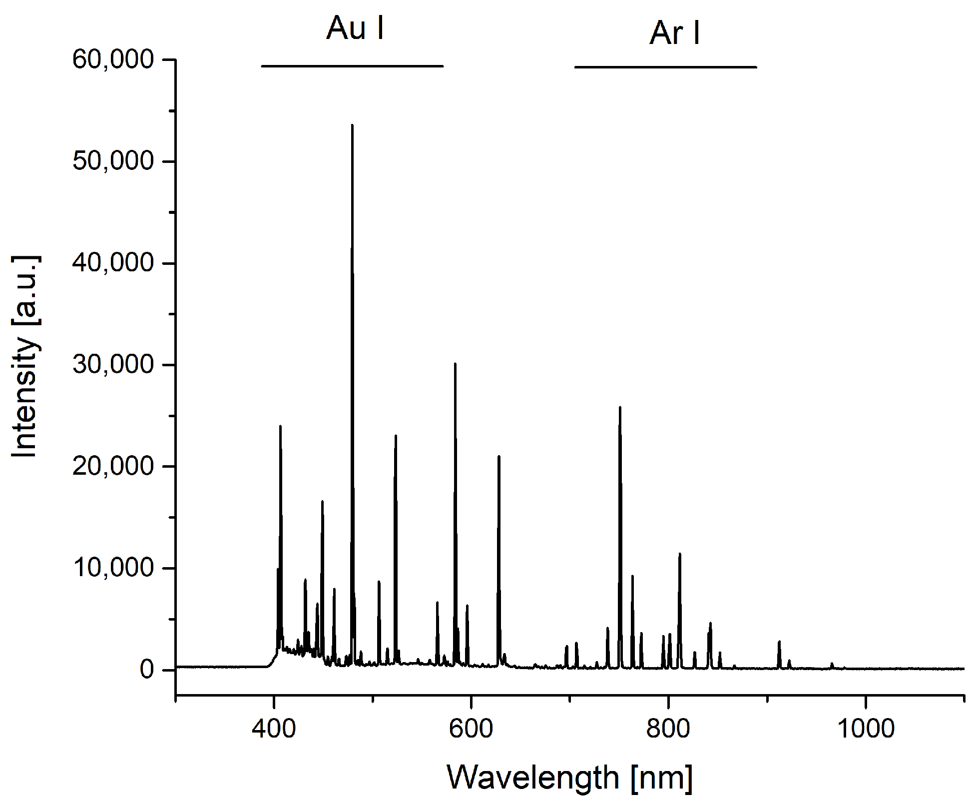
The spectrum of the process can be seen in Figure 2. The argon- and gold peaks are clearly visible, with Au I-peaks between 400 and 700 nm, and Ar I-peaks at wavelengths above 700 nm. Only Au I-peaks are visible in the spectrum. No Au II-peaks could be found, despite Au II peaks being present in the spectrum above 400 nm, albeit no strong intensity could have been expected. As the lower end of the spectrum ends at about 390 nm wavelength, and most of Au II-peaks are found at wavelengths below 390 nm, it is possible that Au II occurs, but could not be measured. The intensity of several Au I peaks is comparable to the intensity of the brightest Ar I peak. Having roughly one peak per color of the spectrum, this results in a white glowing plasma. While the Ar I peaks are clearly visible, Ar II could hardly be found with only one possible faint peak.

3.3. Surface and Cross-Cut Morphology of the Gold Layers

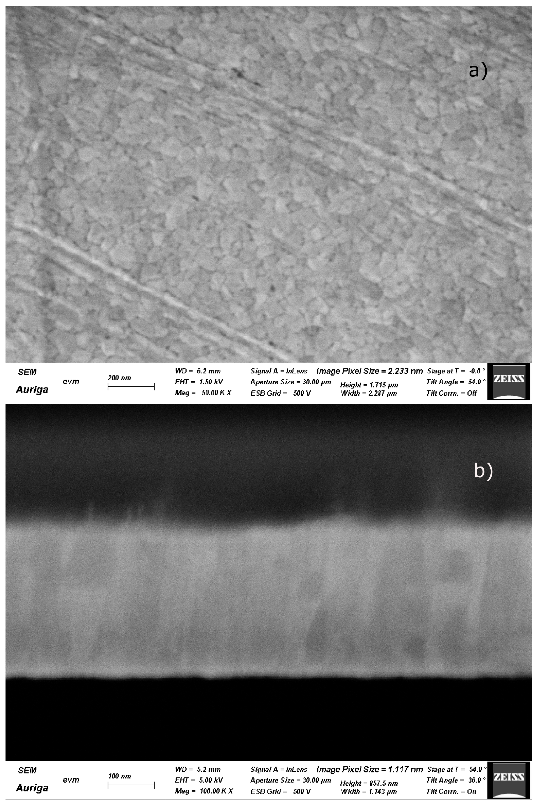
The gold layer was pictured with a scanning electron microscope (SEM) and can both be seen Figure 3. The upper Figure 3a shows the layer 50.000-fold magnified and the lower Figure 3b shows a cut through the layers with a 100.000-fold magnification. A uniform surface can be seen with crystals, having little variation in size, with a width of around 50 nm, thus having a size not to far off from the thickness of the film. No formation of domes is evident from the surface as no crystals with a relatively bigger size compared to the surrounding crystals can be seen. The lower figure shows a cut through the layer that was achieved via focused ion beam (FIB). It is not clear whether the dark areas are voids or not. Surface and cross-cut morphology resemble bulk material.

3.4. Scratch Test

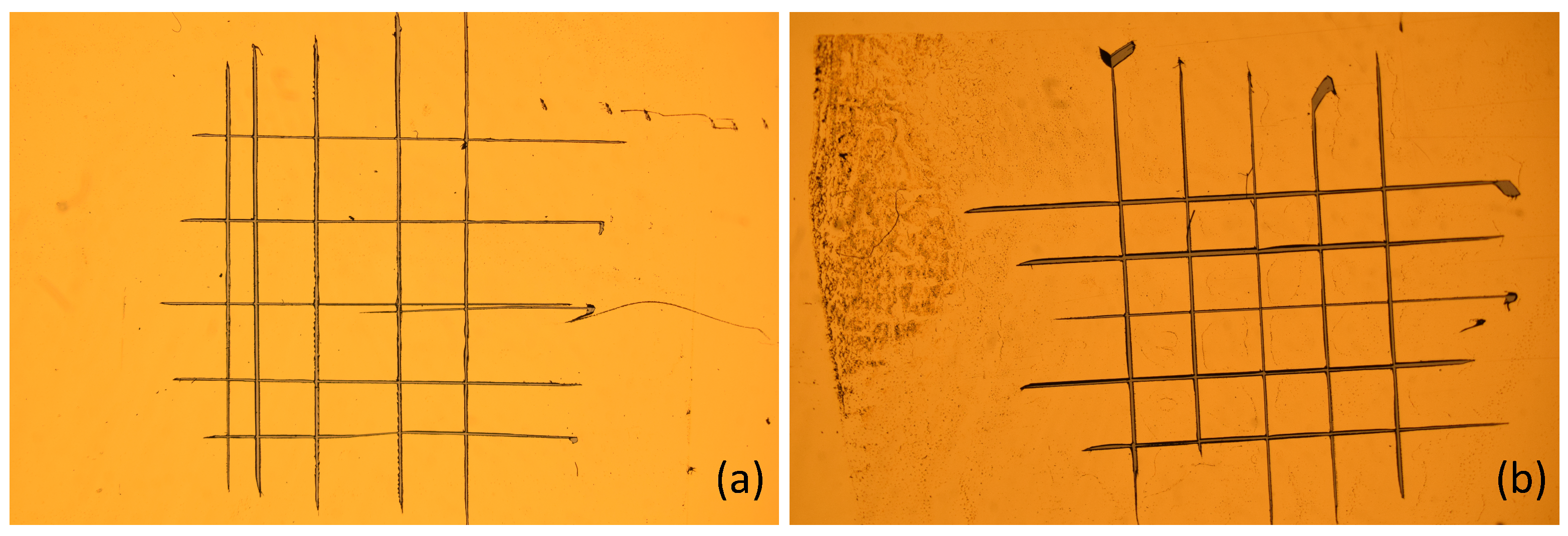
In Figure 4, the results of a scratch test can be seen. The cuts were made with a scalpel and a ruler to ensure that the cuts were straight. The distance between the cuts equals approximately 1 mm. At least five parallel cuts were made with five more in the perpendicular direction. Kapton-tape was applied on the cuts that can be seen in the left Figure 4a, while commercially available adhesive tape was used for the cuts in the right Figure 4b. Shortly after application, the tapes were lifted from the surface. As can be seen, the results are satisfactory. No chipping off or loss of gold layer can be seen in both cases. Both the Kapton-tape and the adhesive film could be lifted off the surface without problems. As can be seen in the right figure, the adhesion between the gold layer and the PI-substrate was so good that residues of the adhesive film were left on the gold surface after the adhesive film was removed.

4. Conclusions

HIPIMS can be used for metallization of Polyimide with gold. This is important, because HIPIMS allows for the omission of adhesive chromium layers and deposition of gold directly onto polyimide, for gold layer thicknesses typical for neural implants. At the same time, it is noteworthy that even at high voltages, only minor ionization of argon takes place, and it remains unclear whether gold is ionized. The resulting gold layer adheres to a polyimide substrate and appears dense in SEM-images.

Author Contributions

Conceptualization, W.L. and J.G.; methodology, J.G.; resources, W.L.; data curation, J.G.; writing—original draft preparation, J.G.; writing—review and editing, W.L.; visualization, J.G.; supervision, W.L.; project administration, J.G.; funding acquisition, W.L. All authors have read and agreed to the published version of the manuscript.

Funding

This work was funded by the DFG, project number 40101397.

Institutional Review Board Statement

Not applicable.

Informed Consent Statement

Not applicable.

Data Availability Statement

Not applicable.

Acknowledgments

We are grateful for the fruitful discussions with Andreas Schander, the help of Eva Maria Meyer who made the SEM images and Michael Skowrons, who helped with grammar and orthography.

Conflicts of Interest

The authors declare no conflict of interest.

Abbreviations

The following abbreviations are used in this manuscript:
ABSAcrylonitrile butadiene styrene
ECoGElectrocorticography
FIBFocused Ion Beam
HIPIMSHigh Power Impulse Magnetron Sputtering
NISTNational Institute of Standards and Technology
OESOptical Emission Spectroscopy
PETPolyethylene terephthalate
PIPolyimide
PPX-CParylene-C
PVDPhysical Vapour Deposition
SEMScanning Electron Microscope
SU-8Polymer

References

  1. Nandra, M.S.; Lavrov, I.A.; Edgerton, V.R.; Tai, Y. A parylene-based microelectrode array implant for spinal cord stimulation in rats. In Proceedings of the 2011 IEEE 24th International Conference on Micro Electro Mechanical Systems, Cancun, Mexico, 23–27 January 2011; pp. 1007–1010. [Google Scholar]
  2. Biswas, S.; Sikdar, D.; Das, D.; Mahadevappa, M.; Das, S. PDMS based multielectrode arrays for superior in-vitro retinal stimulation and recording. Biomed. Microdevices 2017, 19, 1–14. [Google Scholar] [CrossRef] [PubMed]
  3. Rousche, P.J.; Pellinen, D.S.; Pivin, D.P.; Williams, J.C.; Vetter, R.J.; Kipke, D.R. Flexible polyimide-based intracortical electrode arrays with bioactive capability. IEEE Trans. Biomed. Eng. 2001, 48, 361–371. [Google Scholar] [CrossRef] [PubMed]
  4. Merriam, S.M.E.; Srivannavit, O.; Gulari, M.N.; Wise, K.D. A three-dimensional 64-site folded electrode array using planar fabrication. J. Microelectromech. Syst. 2011, 20, 594–600. [Google Scholar] [CrossRef]
  5. Seymour, J.P.; Elkasabi, Y.M.; Chen, H.; Lahann, J.; Kipke, D.R. The insulation performance of reactive parylene films in implantable electronic devices. Biomaterials 2009, 30, 6158–6167. [Google Scholar] [CrossRef] [Green Version]
  6. Huang, R.K.-J. Flexible Neural Implants. Ph.D. Thesis, California Institute of Technology, Pasadena, CA, USA, 2011. [Google Scholar]
  7. Chen, C.; Chuang, S.; Su, H.; Hsu, W.; Yew, T.; Chang, Y.; Yeh, S.; Yao, D. A three-dimensional flexible microprobe array for neural recording assembled through electrostatic actuation. Lab Chip 2011, 11, 1647–1655. [Google Scholar] [CrossRef]
  8. Kim, E.G.R.; John, J.K.; Tu, H.; Zheng, Q.; Loeb, J.; Zhang, J.; Xu, Y. A hybrid silicon–paryleneneural probe with locally flexible regions. Sens. Actuators B Chem. 2014, 195, 416–422. [Google Scholar] [CrossRef]
  9. Shin, S.; Kim, J.; Jeong, J.; Gwon, T.M.; Lee, S.; Kim, S.J. Novel four-sided neural probe fabricated by a thermal lamination process of polymer films. J. Neurosci. Methods 2017, 278, 25–35. [Google Scholar] [CrossRef]
  10. Tsang, W.M.; Je, M. Flexible electrode for implantable neural devices. Neural Comput. Neural Devices Neural Prosthes. 2014, 10, 121–156. [Google Scholar]
  11. Williamson, A.; Ferro, M.; Leleux, P.; Ismailova, E.; Kaszas, A.; Doublet, T.; Quilichini, P.; Rivnay, J.; Rózsa, B.; Katona, G. Localized neuron stimulation with organic electrochemical transistors on delaminating depth probes. Adv. Mater. 2015, 27, 4405–4410. [Google Scholar] [CrossRef]
  12. Lecomte, A.; Degache, A.; Descamps, E.; Dahan, L.; Bergaud, C. In vitro and in vivo biostability assessment of chronically-implanted Parylene C neural sensors. Sens. Actuators B Chem. 2017, 251, 1001–1008. [Google Scholar] [CrossRef]
  13. Baek, D.; Lee, E.; Moon, J.; Choi, J.H.; Pak, J.J.; Lee, S. Polyimide-based multi-channel arrayed electrode for measuring EEG signal on the skull of mouse. In Proceedings of the 2009 Annual International Conference of the IEEE Engineering in Medicine and Biology Society, Minneapolis, MN, USA, 2–6 September 2009; pp. 7022–7025. [Google Scholar]
  14. Márton, G. Development and Characterization of Novel Microelectrode Arrays for Neurophysiology. Ph.D. Thesis, Semmelweis University, Budapest, Hungary, 2015. [Google Scholar]
  15. Kireev, D.; Montes, V.R.; Stevanovic, J.; Srikantharajah, K.; Offenhäusser, A. N3-MEA probes: Scooping neuronal networks. Front. Neurosci. 2019, 13, 320. [Google Scholar] [CrossRef] [PubMed]
  16. Gymama, S.; Matthew, R.; Joel, T.; Chen, J. Neuroelectronic device process development and challenge. In Optical Microlithography XXX; Andreas, E., Jongwook, K., Eds.; SPIE: Bellingham, WA, USA, 2017; Volume 10147, p. 101470W. [Google Scholar]
  17. Tolstosheeva, E.; Hoeffmann, J.; Pistor, J.; Rotermund, D.; Schellenberg, T.; Boll, D.; Hertzberg, T.; Gordillo-Gonzalez, V.; Mandon, S.; Peters-Drolshagen, D.; et al. Towards a wireless and fully-implantable ECoG system. In Proceedings of the 2013 Transducers & Eurosensors XXVII: The 17th International Conference on Solid-State Sensors, Actuators and Microsystems (TRANSDUCERS & EUROSENSORS XXVII), Barcelona, Spain, 16–20 June 2013; pp. 384–387. [Google Scholar]
  18. Rodri, F.J.; Ceballos, D.; Schu, M.; Valero, A.; Valderrama, E.; Stieglitz, T.; Navarro, X. Polyimide cuff electrodes for peripheral nerve stimulation. J. Neurosci. Methods 2000, 98, 105–118. [Google Scholar]
  19. Tintelott, M.; Schander, A.; Lang, W. Understanding Electrical Failure of Polyimide-Based Flexible Neural Implants: The Role of Thin Film Adhesion. Polymers 2022, 14, 3702. [Google Scholar] [CrossRef] [PubMed]
  20. Deku, F.; Frewin, C.L.; Stiller, A.; Cohen, Y.; Aqeel, S.; Joshi-Imre, A.; Black, B.; Gardner, T.J.; Pancrazio, J.J.; Cogan, S.F. Amorphous silicon carbide platform for next generation penetrating neural interface designs. Micromachines 2018, 9, 480. [Google Scholar] [CrossRef] [PubMed] [Green Version]
  21. Schander, A.; Stemmann, H.; Tolstosheeva, E.; Roese, R.; Biefeld, V.; Kempen, L.; Kreiter, A.K.; Lang, W. Design and fabrication of novel multi-channel floating neural probes for intracortical chronic recording. Sens. Actuators A Phys. 2016, 247, 125–135. [Google Scholar] [CrossRef]
  22. Nwankire, C.E.; Venkatanarayanan, A.; Forster, R.J.; Ducrée, J. Enhanced gold-to-polymer adhesion for integrated electrochemical biosensing on cost-efficient lab-on-achip cartridges. In Proceedings of the 19th International Conference on Miniaturized Systems for Chemistry and Life Sciences, Gyeongju, Republic of Korea, 25–29 October 2015. [Google Scholar]
  23. Moazzez, B.; O’Brien, S.M.; Merschrod, E. Improved adhesion of gold thin films evaporated on polymer resin: Applications for sensing surfaces and MEMS. Sensors 2013, 13, 7021–7032. [Google Scholar] [CrossRef] [PubMed]
  24. Von Metzen, R.P.; Stieglitz, T. The effects of annealing on mechanical, chemical, and physical properties and structural stability of Parylene C. Biomed. Microdevices 2013, 15, 727–735. [Google Scholar] [CrossRef]
  25. Li, W.; Rodger, D.; Menon, P.; Tai, Y. Corrosion behavior of parylene-metal-parylene thin films in saline. ECS Trans. 2008, 11, 1. [Google Scholar] [CrossRef] [Green Version]
  26. Wu, P.Y.; Lin, C.H.; Chen, C.-M. Study of surface metallization of polyimide film and interfacial characterization. Metals 2017, 7, 189. [Google Scholar] [CrossRef] [Green Version]
  27. Yoon, S.S.; Kim, D.O.; Park, S.C.; Lee, Y.K.; Chae, H.Y.; Jung, S.B.; Nam, J.-D. Direct metallization of gold patterns on polyimide substrate by microcontact printing and selective surface modification. Microelectron. Eng. 2008, 85, 136–142. [Google Scholar] [CrossRef]
  28. Huang, S.-E.; Shen, F.-Y.; Dow, W.-P. Polyimide metallization using nickel nano-film as both catalyst and barrier layer of copper electroless deposition. J. Electrochem. Soc. 2019, 166, D843. [Google Scholar] [CrossRef]
  29. Ma, Q.; Moldovan, N.; Mancini, D.C.; Rosenberg, R.A. Synchrotron-radiation-induced, selective-area deposition of gold on polyimide from solution. Appl. Phys. Lett. 2000, 76, 2014–2016. [Google Scholar] [CrossRef]
  30. Zahavi, J.; Rotel, M.; Katz, D.; Levine, S. UV Laser-Induced Metallization of Polyimide from Electroplating Solution. Met. Plast. 1 1989, 55–68. [Google Scholar]
  31. Pflüger, S.; Wehner, M.; Jansen, F.; Kruck, T.; Lupp, F. Deposition of gold on polyimide from solutions. Appl. Surf. Sci. 1995, 86, 504–508. [Google Scholar] [CrossRef]
  32. Basarir, F.; Yoon, T.-H. Preparation of gold patterns on polyimide coating via layer-by-layer deposition of gold nanoparticles. J. Colloid Interface Sci. 2010, 352, 11–18. [Google Scholar] [CrossRef] [PubMed]
  33. Kong, Y.; Shao, J.; Wang, W.; Chen, Z.; Chu, H. Surface modification and metallization of polyimide using gold colloids as a seed layer. J. Appl. Polym. Sci. 2009, 111, 2044–2048. [Google Scholar] [CrossRef]
  34. Melentiev, R.; Yudhanto, A.; Tao, R.; Vuchkov, T.; Lubineau, G. Metallization of polymers and composites: State-of-the-art approaches. Mater. Des. 2022, 110958. [Google Scholar] [CrossRef]
  35. Kouznetsov, V.; Macak, K.; Schneider, J.M.; Helmersson, U.; Petrov, I. A novel pulsed magnetron sputter technique utilizing very high target power densities. Surf. Coatings Technol. 1999, 122, 290–293. [Google Scholar] [CrossRef]
  36. Mozgrin, D.V.; Fetisov, I.K.; Khodachenko, G.V. High-current low-pressure quasi-stationary discharge in a magnetic field: Experimental research. Plasma Phys. Rep. 1995, 21, 400–409. [Google Scholar]
  37. Ehiasarian, A.P. High-power impulse magnetron sputtering and its applications. Pure Appl. Chem. 2010, 82, 1247–1258. [Google Scholar] [CrossRef]
  38. Gudmundsson, J.T.; Brenning, N.; Lundin, D.; Helmersson, U. High power impulse magnetron sputtering discharge. J. Vac. Sci. Technol. A Vac. Surfaces Film. 2012, 30, 030801. [Google Scholar] [CrossRef] [Green Version]
  39. Eichenhofer, G.; Fernandez, I.; Wennberg, A. Industrial Use of HiPIMS up to Now and a Glance into the Future, A Review by a Manufacturer Introduction of the hiP-V hiPlus Technology. Univers. J. Phys. Appl. 2017, 11, 73–79. [Google Scholar] [CrossRef]
  40. Bandorf, R.; Waschke, S.; Carreri, F.C.; Vergöhl, M.; Grundmeier, G.; Bräuer, G. Direct metallization of PMMA with aluminum films using HIPIMS. Surf. Coatings Technol. 2016, 290, 77–81. [Google Scholar] [CrossRef]
  41. Kelly, P.J.; Barker, P.M.; Ostovarpour, S.; Ratova, M.; West, G.T.; Iordanova, I.; Bradley, J.W. Deposition of photocatalytic titania coatings on polymeric substrates by HiPIMS. Vacuum 2012, 86, 1880–1882. [Google Scholar] [CrossRef]
  42. Chen, Y.-H.; Hsu, C.-C.; He, J.-L. Antibacterial silver coating on poly (ethylene terephthalate) fabric by using high power impulse magnetron sputtering. Surf. Coatings Technol. 2013, 232, 868–875. [Google Scholar] [CrossRef] [Green Version]
  43. Zhang, D.; Zuo, X.; Wang, Z.; Li, H.; Chen, R.; Wang, A.; Ke, P. Comparative study on protective properties of CrN coatings on the ABS substrate by DCMS and HiPIMS techniques. Surf. Coatings Technol. 2020, 394, 125890. [Google Scholar] [CrossRef]
  44. Bandorf, R.; Waschke, S.; Vergöhl, M.; Grundmeier, G.; Bräuer, G. Haftfeste Direktmetallisierung von Kunststoffen durch Beschichtung mit Ionen: Neue Anwendungsfelder für HIPIMS Technologie. Vak. Forsch. Prax. 2015, 27, 18–23. [Google Scholar] [CrossRef]
  45. Fantz, U. Basics of plasma spectroscopy. Plasma Sources Sci. Technol. 2006, 15, S137. [Google Scholar] [CrossRef] [Green Version]
  46. Wu, B.; Haehnlein, I.; Shchelkanov, I.; McLain, J.; Patel, D.; Uhlig, J.; Jurczyk, B.; Leng, Y.; Ruzic, D.N. Cu films prepared by bipolar pulsed high power impulse magnetron sputtering. Vacuum 2018, 150, 216–221. [Google Scholar] [CrossRef]
  47. NIST Atomic Spectra Database. Available online: https://physics.nist.gov/PhysRefData/ASD/lines_form.html (accessed on 6 January 2023).
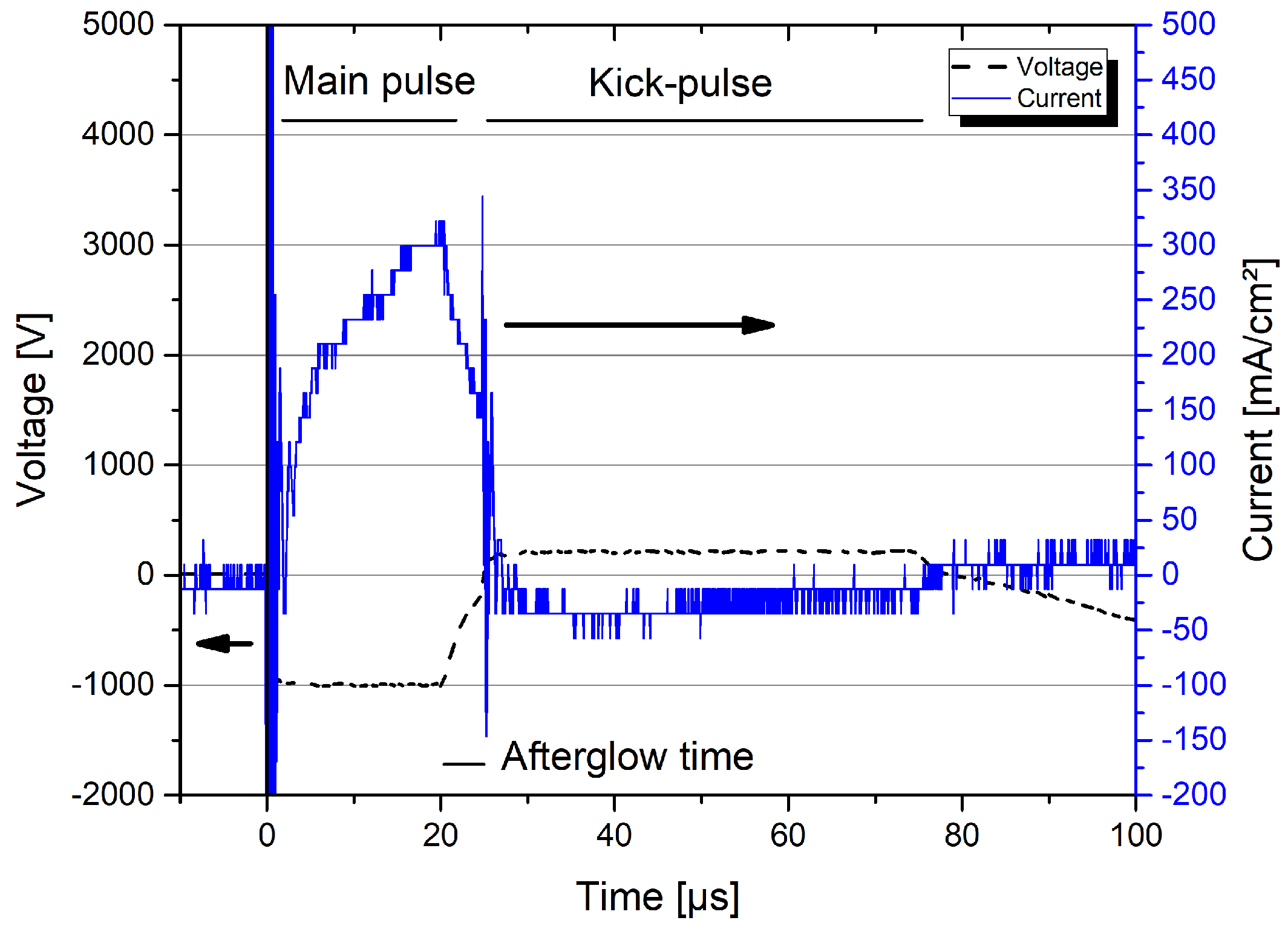
Figure 1. Voltage (dashed line, scale at the left) and current (straight blue line, scale at the right) waveforms during a pulse.
Coatings 13 00250 g001
Figure 2. Spectrum of process with mainly Au I and Ar I peaks. The spectrum encompasses the wavelength range between roughly 395 nm and 1100 nm.
Coatings 13 00250 g002
Figure 3. Gold layer imaged with a scanning electron microscope. (a) The upper image shows the surface of the gold film. (b) The lower image shows a cut through the gold film.
Coatings 13 00250 g003
Figure 4. (a) Gold layer after Kapton-tape was applied. (b) Gold layer after Tesa-film was applied. Residues of the adhesive film can be seen in the upper left corner.
Coatings 13 00250 g004
Disclaimer/Publisher’s Note: The statements, opinions and data contained in all publications are solely those of the individual author(s) and contributor(s) and not of MDPI and/or the editor(s). MDPI and/or the editor(s) disclaim responsibility for any injury to people or property resulting from any ideas, methods, instructions or products referred to in the content.