Article

Effects of Doping Ratio and Thickness of Indium Tin Oxide Thin Films Prepared by Magnetron Sputtering at Room Temperature

1
BAIMTEC Material Co., Ltd., Beijing 100095, China
2
Beijing Engineering Research Centre of Advanced Structural Transparencies for the Modern Traffic System, Beijing 100095, China
*
Author to whom correspondence should be addressed.
Coatings 2023, 13(12), 2016; https://doi.org/10.3390/coatings13122016
Submission received: 4 November 2023 / Revised: 20 November 2023 / Accepted: 27 November 2023 / Published: 29 November 2023

Abstract

:
Transparent conducting films on polymeric substrates are increasingly applied in diverse novel displays and flexible electronics. In this paper, indium tin oxide films on polymeric substrates were deposited by magnetron sputtering using ceramic targets with different doping ratios. These films were characterized by X-ray photoelectron spectroscopy, X-ray diffractometer, atomic force microscopy, spectroscopic ellipsometry, spectrophotometer, sheet resistance meter, and the Hall effect measurement. In terms of transparency and conductivity, the results have shown that the doping ratio played a less important role in determining the optical properties, while the electrical properties were significantly influenced. It was found that, when the thickness was less than 130 nm, these films with the nominal doping ratio of 95:5 (wt. %) demonstrated higher electrical conductivity compared to those with 90:10 (wt. %), which were widely used in industry. Therefore, for the flexible polymeric substrate, the target with a doping ratio of 95:5 (wt. %) could be suitable to achieve high electrical conductivity.

1. Introduction

Combined with high visible transparency and direct current (DC) electrical conductivity, transparent conducting oxide (TCO) films have been applied in depth in various commercial fields, including flat-panel displays, solar cells, and energy-efficient windows, such as electrochromic windows [1,2]. Today, there is growing interest in flexible devices, because they would be more robust, light weight, conformable, and potentially cheaper to manufacture by roll-to-roll processing [1,3,4].
While as the synonym of TCO, indium tin oxide (ITO, basically with SnO2 doping ratio 10 wt. %) coated transparent plastic is commercially available, film performance is generally inferior to ITO on inorganic glass, which enables film growth or post-annealing at high temperature, reducing electrical resistivity (1.5 × 10⁻⁴ Ω·cm). On plastic, the resistivity of ITO film is typically not less than 6 × 10⁻⁴ Ω·cm. But low resistance and smooth morphology are essential in finely patterned, high-resolution dynamic displays [5,6,7]. Currently, ITO thin films with the 10 wt. % doping ratios have been intensively studied and widely used in industry. However, as we know, tin in amorphous ITO is not activated when deposited near room temperature (RT) [8,9,10,11], the resistivity achieved on typical plastic substrates is ~4× higher (~8 × 10⁻⁴ Ω·cm) than when deposited on glass (>200 °C). Indium oxide with reduced doping concentration could be somewhat better (~4 × 10⁻⁴ Ω·cm) than ITO (10 wt. % SnO2), due to lower scattering for conducting electrons [12,13]. Some reported results are listed in Table 1. Bae et al. reported that [10] the as-deposited ITO obtained even lower resistivity when the tin doping ratio was less than 10 wt. %. By the density functional theory calculation, Tripathi found that [13] the visible transmission would decrease greatly down to 60% when the tin doping ratio was higher than 6%. Kang showed that [14] the lowest resistivity and relatively small stress level was obtained for the film deposited from an ITO target doped with 7 wt. % SnO2. However, only Yang et al. reported [15] that even lower resistivity could be obtained by sputtering ITO ceramic targets with doping metallic tin via co-sputtering. For the convenience of ITO target production, tin is still the favorite doping element although other doping elements have been reported already, e.g., Ti [16], Nb [17], Si [4], and H [18]. In addition, ITO films with thin thickness, i.e., less than 50 nm are of great technological importance in many applications, such as touch panels [7], which is quite different from the thicker ITO (several hundreds of nanometers) on glass for de-icing. In this paper, we have studied the effect of doping ratio and thickness upon the structure, composition and related physical properties of ITO films with three different doping ratios.

2. Materials and Methods

By using the Φ75 × 4 mm ceramic targets backed by copper plate with different doping ratios, i.e., 97:3, 95:5, 90:10 (wt. %) for In2O3:SnO2 (donated as ITO-9703, ITO-9505, ITO-9010), with purity of 99.99%, three-type ITO thin films were deposited on silicon wafer and polyethylene terephthalate (PET) substrates using DC magnetron sputtering at ambient temperature. Detailed deposition parameters are shown in Table 2. XRD analysis was performed in asymmetric 2θ (incident angle being 1°) configuration using a Rigaku diffractometer (D/max 2500, Rigaku, Tokyo, Japan) to characterize the crystal structure of the films. The compositions and chemical states after surface contamination removal using Ar+ beam etching 3 nm and 100 nm, respectively, were determined by X-ray photoelectron spectroscopy (XPS, PHI Quantera SXM, ULVAC-PHI, Tokyo, Japan) using C 1s 284.8 eV as a reference. The surface morphologies were measured by atomic force microscopy (SOLVER Nano, NT-MDT, Moscow, Russia). Spectroscopic ellipsometry (300~800 nm, SE800, SENTECH, Berlin Germany) was employed to evaluate the optical constants and thickness. The sheet resistance measurements were performed using a four-point probe (SD510, NAGY, Gäufelden, Germany). Hall mobility and carrier concentration measurements were made using the van der Pauw method at RT with a field strength of 5000 G. The optical transmission and reflectance measurements were made using a UV-Vis-NIR spectrophotometer in a double-beam configuration (Cary 5000, Varian, Palo Alto, CA, USA).

3. Results

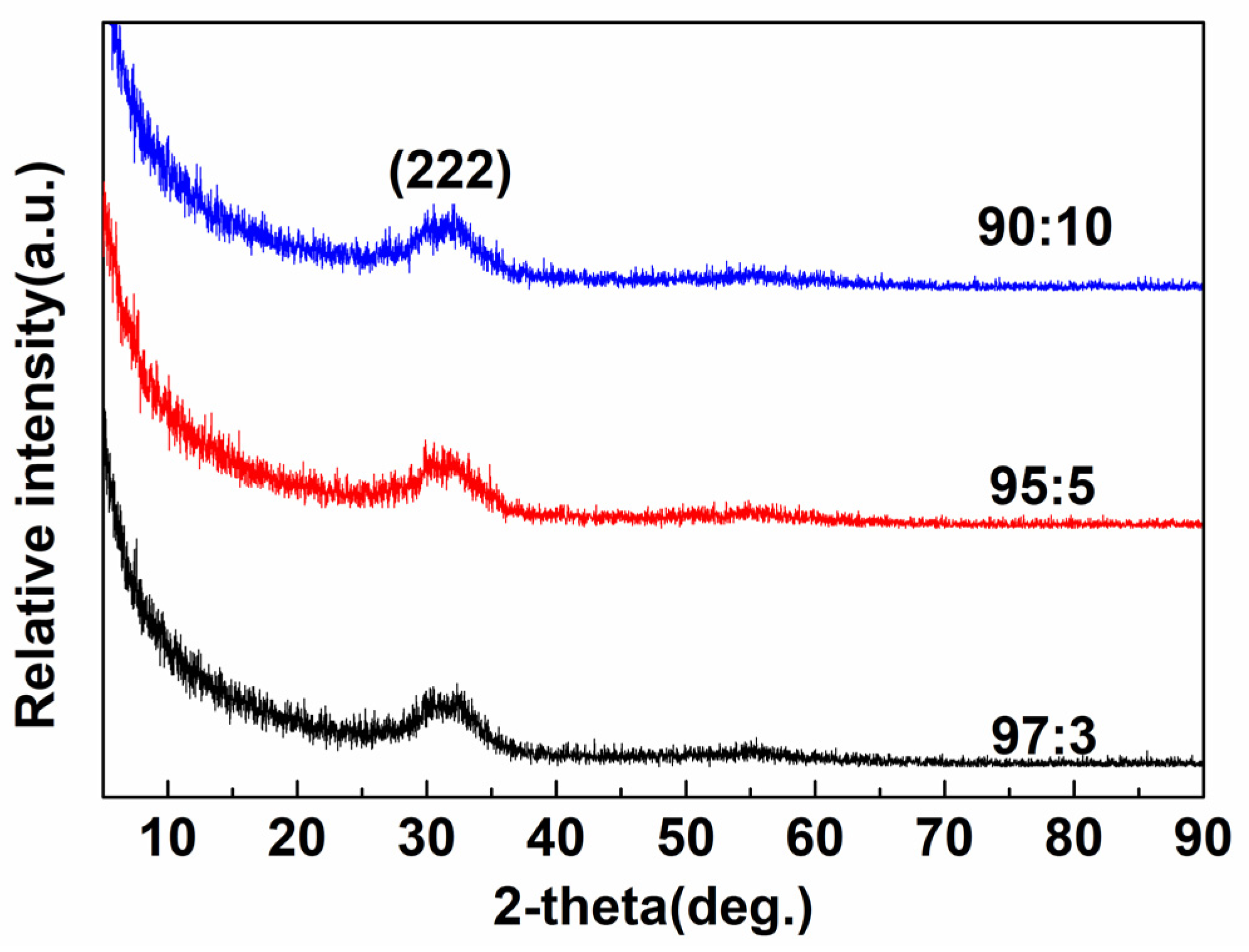
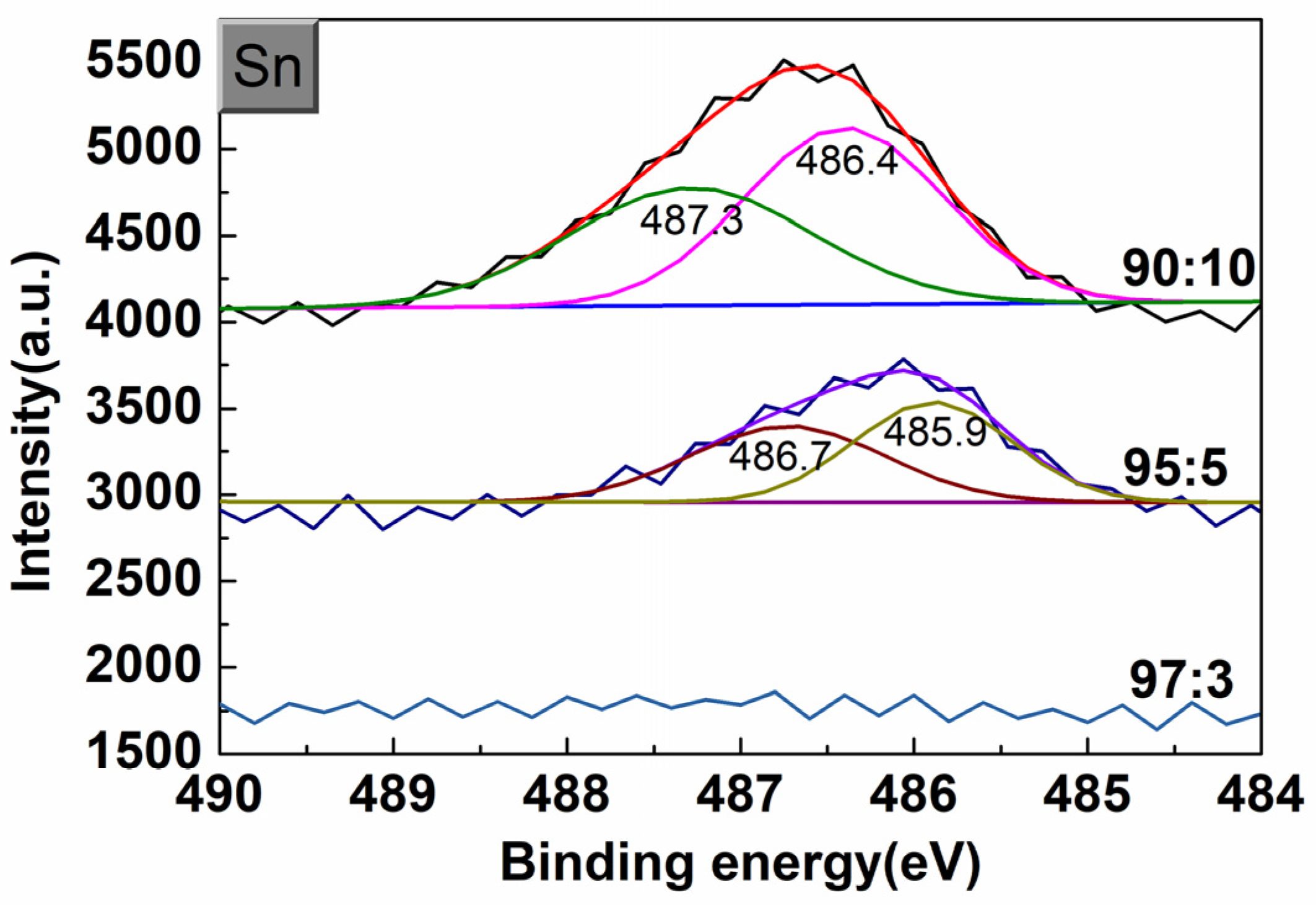
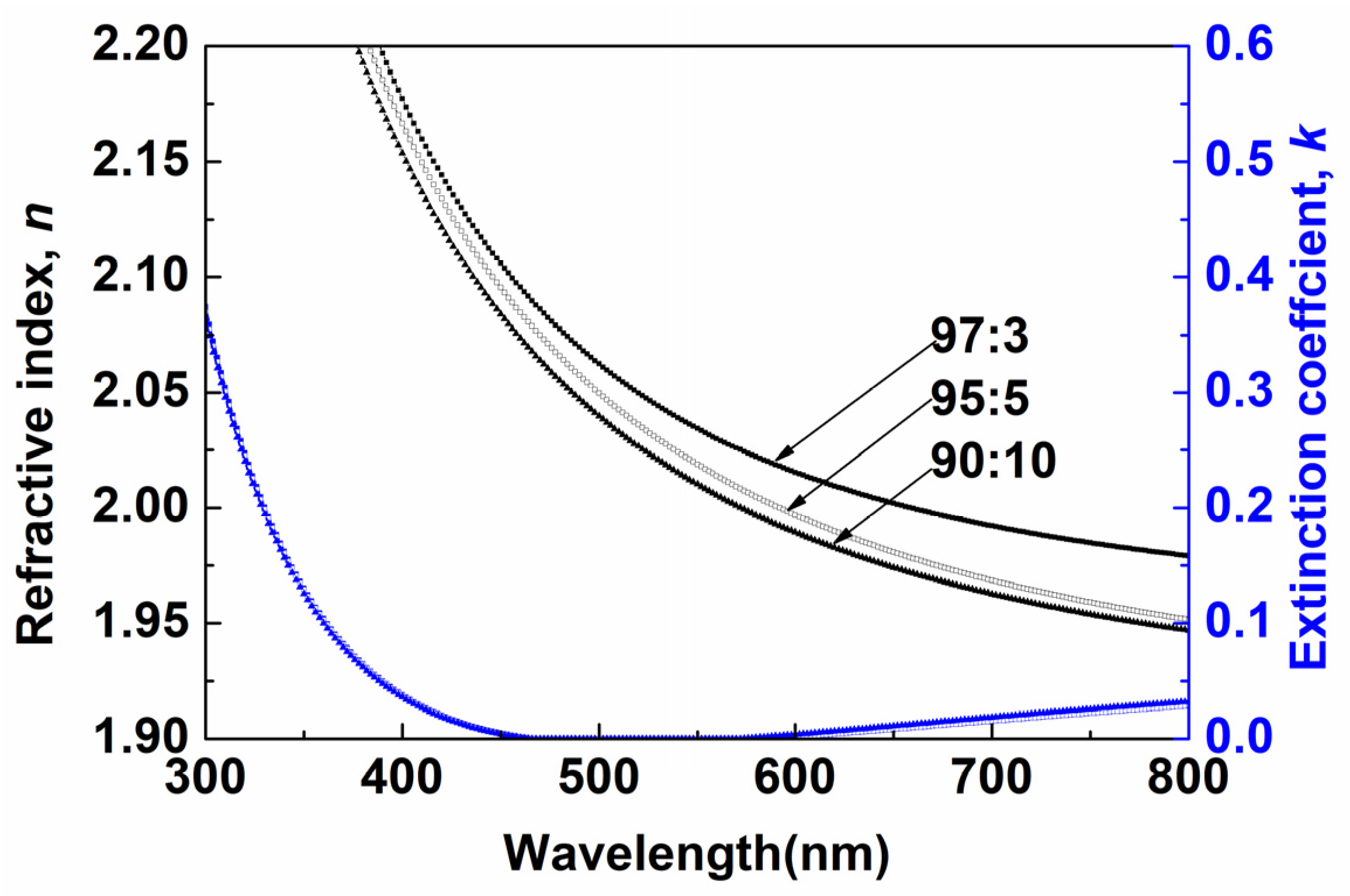
3.1. Effect of Doing Ratio

All ITO films were deposited at ambient temperature, and no extra heating treatments (substrate heating or annealing) were imposed. Figure 1 indicated that, for all ITO films with a thickness of about 125 nm, only a blunt peak (222) appeared in the spectra regardless of different doping ratios. So, all films were nanocrystalline and amorphous.
It is known that the composition in films was always different from the one in targets. The tin content in three-type ITO films was generally slightly lower than that in targets. All these data are summarized in Table 2. In the case of ITO-9703, the tin concentration was close to the detection limit of XPS, as shown in Figure 2. According to reference [20], the binding energy 485.3 eV, 486.2 eV, and 486.7 eV correspond to Sn3O4, SnO, and SnO2 phases. From Figure 2, it was indicated that the content of the SnO2 phase in actual ITO films was increasing.
Figure 3 illustrates the decreasing root mean square (RMS) surface roughness for higher doping concentrations from 1.60 nm to 0.40 nm. From the AFM data, we observe that the grain size in room-temperature grown films decreases with the addition of SnO2. It was implied that during sputtering growth, Sn atoms acted as nucleation sites.
ITO films exhibited normal dispersion as shown in Figure 4. Due to the visible transparency, the optical constants of ITO films could be modeled by the Cauchy model and the Sellmier model. In Figure 4, it was demonstrated that the refractive index was increasing from 2.01 to 2.03 at 550 nm when the doping ratio was increasing. Meanwhile, the extinction coefficients were kept at less than 0.05 in the whole visible region.
The origin of n-type electrical conductivity in ITO films was either from intrinsic doping such as oxygen vacancy (VO) or extrinsic doping such as Sn4+ substituting In3+. When the depositing temperature was RT, only amorphous or nano-crystalline ITO could be obtained, and compared to that deposited at higher temperatures, the higher electrical resistivity could be attributed to the non-activity of Sn doping [8,9]. As shown in Table 3, different from the conventional ITO-9010 which used to show the highest conductivity, ITO-9505 films showed lower electrical resistivity which was mainly derived from higher carrier concentration. From the formula of the electron mean free path (eMPF),
L = 3 π 2 1 / 3 h / e 2 ρ 1 N 2 / 3
the calculated eMPFs were 17.24, 29.90, and 28.83 nm. The higher conductivity of ITO-9505 films also was beneficial from comparatively longer eMPF. More fine characterization tools should be employed in the future to unveil this interesting phenomenon. Different from Bae et al. [10] and Dekkers et al. [21], these results were basically consistent with Kang et al.’s report [14]. It seemed that the Sn dopant was not entirely detrimental to the electron conducting when ITO films were amorphous.

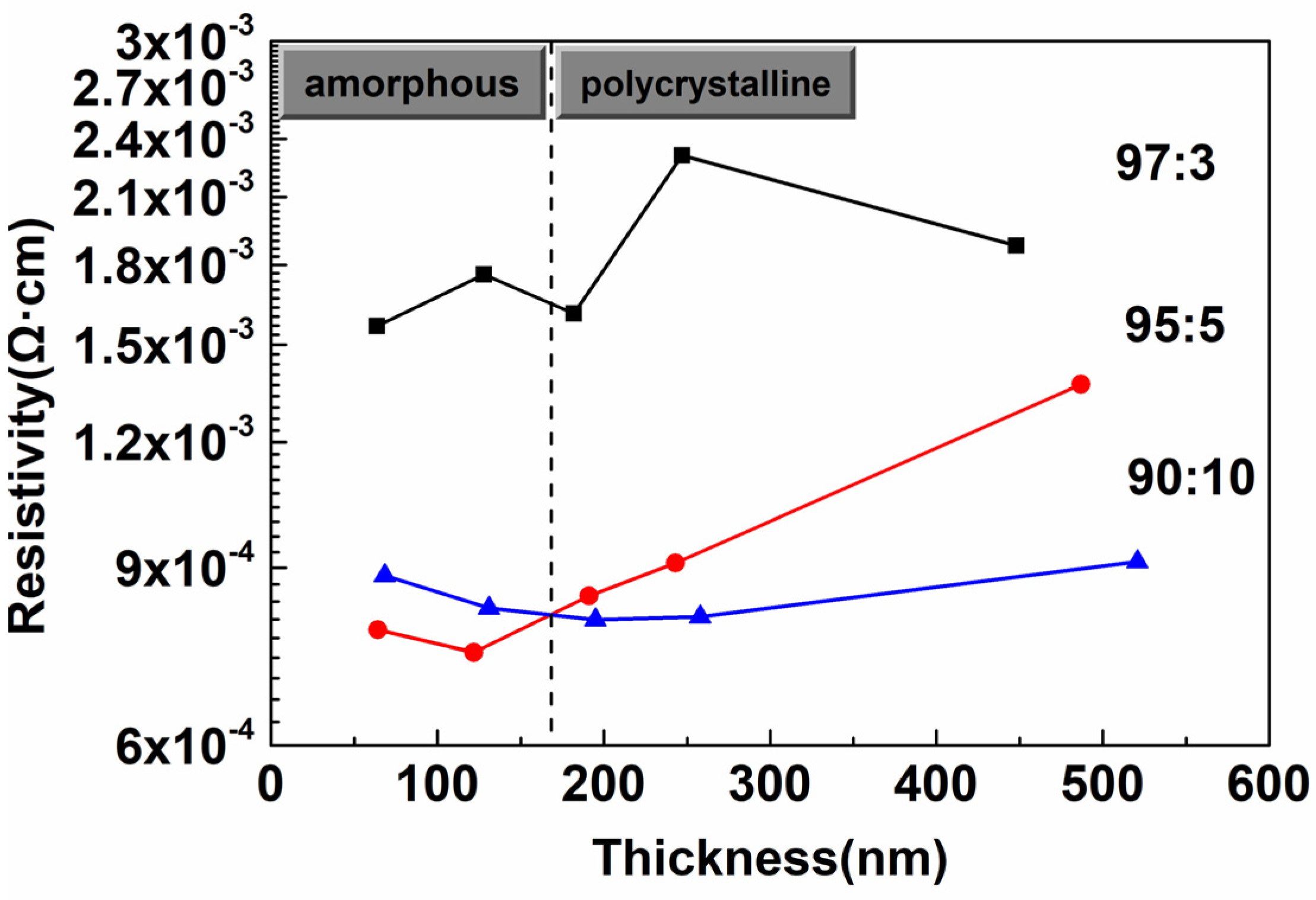
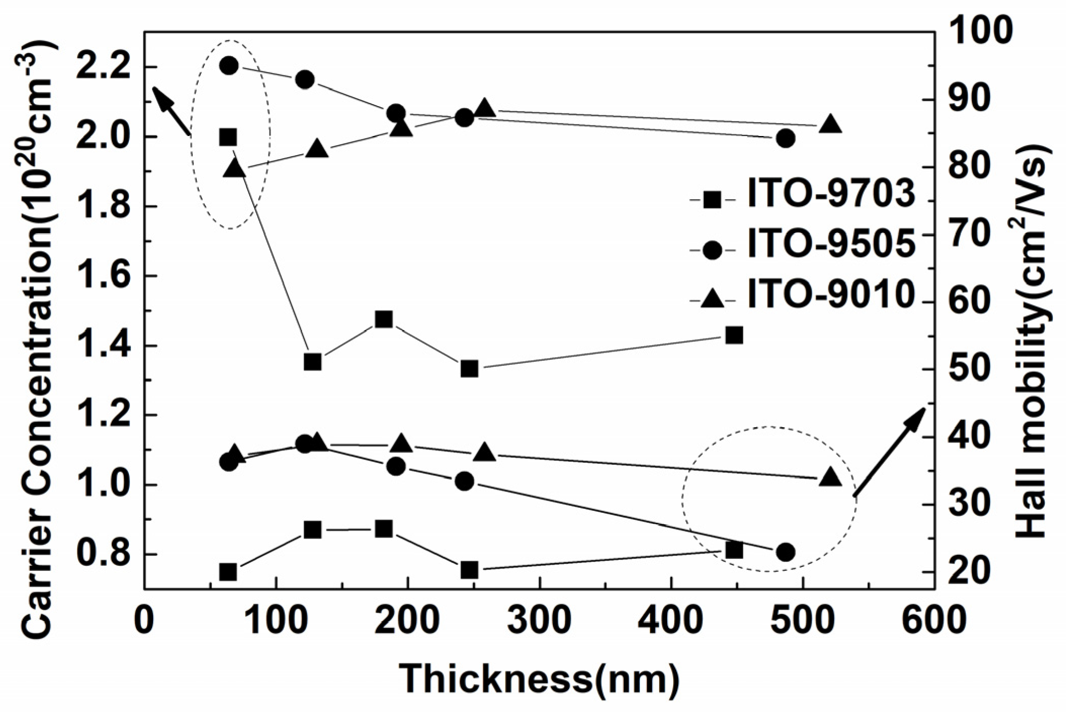
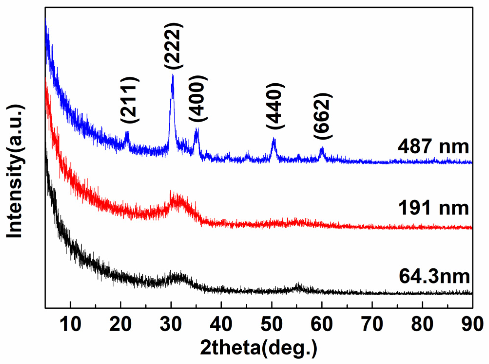
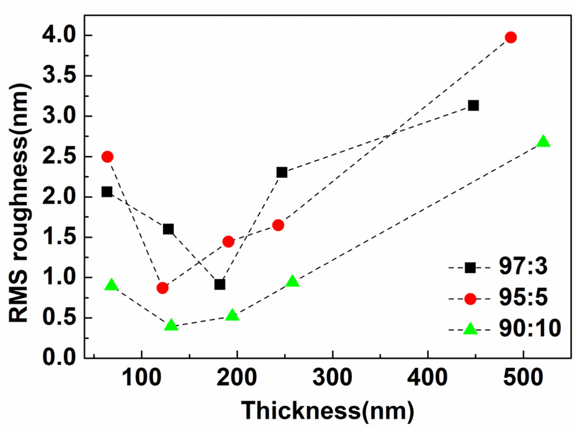
3.2. Effect of Thickness

The thickness could play a remarkable role in determining not only the spectral properties but also the electrical properties of ITO films and the performance of opto-electrical devices [22]. In Figure 5, the specific resistivity of three-type ITO films was changed greatly with the increasing thickness. And the resistivity of ITO-9010 and ITO-9505 films was evidently lower than ITO-9703 films. It was very interesting that there was a critical thickness, dc, that the resistivity of ITO-9505 films was lower than that of ITO-9010 films when the thickness was less than dc, and vice versa. As shown in Table 1, the reported resistivities of ITO films with less than 10 wt. % doping ratio were less than the value listed in Table 2. The main difference in this paper is that deliberately substrate heating or low-temperature annealing (<100 °C) was carried out or extra gas species were fed in the sputtering chamber compared with other researchers [14,15].
According to the electrical resistivity formula ρ = 1/qμne, i.e., the resistivity ρ was determined by carrier charge q, mobility μ, and carrier concentration ne. Generally, the predominance of electrical resistivity was derived from the promotion of both mobility and carrier concentration. As shown in Figure 6, for ITO-9010 and ITO-9505, this resistivity discrepancy was principally arising from the different carrier concentration due to the almost same Hall mobility, i.e., 38.9 cm2V−1s−1, for the two-type films when the thickness was less than dc. This was true in Section 3.1. These experimental results were distinct from other researchers’ results [8,9] and reproduced well.

4. Discussion

ITO is the classical n-type semiconductor that which there were two different generation mechanisms of conducting electrons: intrinsic doping and extrinsic doping. Intrinsic doping means doping naturally, such as, for example, oxygen vacancy VO, etc.; for the latter, it is substitutive doping by tin ions which was dominant for the widely used crystalline ITO films. However, the situation for ITO film deposition at RT was not completely understood yet [9,23,24]. It was generally accepted that VO played a major role in carrier-generating that the double-charged oxygen vacancies could provide two electrons in the conduction band. According to the calculated results [25], only oxygen vacancy could not be responsible for the n-type conductivity in In2O3 due to the energetic instability. Tang et al. [26] proposed that the defect pairs interactions between VO and In interstitial Ini or Sn dopant SnIn would significantly reduce their formation energies, making these donors an important source of n-type conductivity in In2O3. Moreover, by combining with VO, the ionization energies of Ini or a SnIn would be decreased, and then the electrical conductivity was enhanced via the donor–donor binding.
The improvement of ITO-9010 films could be understood from the angle of crystallization when the thickness was more than dc. The tin donor was activated by crystallization due to the increase in thickness, as indicated in Figure 7, but not due to the substrate heating or annealing treatment. For a thickness less than dc, a moderate doping ratio was required in order to obtain higher electrical conductivity, seemly owing to the formation of energetically favorable VO-Ini and VO-SnIn proposed by Tang et al. [17] because too high a doping ratio would lead to lower carrier concentration and a lower doping ratio to more tin substitution inactivated. Apparently, the trend of electrical resistivity was coherent with the conversion from an amorphous to a crystalline state. Here, defect chemistry should be further studied quantitatively [27,28,29].
To some extent, surface morphologies would influence the properties of ITO films. It was demonstrated in Figure 8 that the RMS (root mean square) roughness of ITO film surfaces extracted from Figure 3 decreased when the thickness was less than dc, and vice versa. This experimental phenomenon could be explained by the competition between grain growth and surface roughening. At the initial stage, deposited ITO might be discontinued and form islands. With the increasing thickness, the more islands coalesced; the surface was flattened, as exhibited in Figure 8. Then, the surface became rougher when the thickness further increased, concomitantly, the grain size was increased which was confirmed with the comparatively sharp diffraction peak in Figure 7. From Figure 8, the RMS roughness of ITO-9505 films was shown comparatively lower roughness while keeping slightly lower resistivity, when the thickness was less than dc, while ITO-9010 films would be beneficial from this feature when the thickness was more than dc.

5. Conclusions

Indium tin oxide films with different nominal doping ratios (3 wt. %, 5 wt. %, and 10 wt. % SnO2) were deposited by direct current magnetron sputtering at room temperature. It was found that without substrate heating or annealing, For a thickness of about or less than 125 nm, indium tin oxide films with a doping ratio of 5 wt. % demonstrated the lowest electrical resistivity among three-type amorphous indium tin oxide films, which would be suitable for the touch panel application which requires low electrical resistivity and less thickness.

Author Contributions

Conceptualization, X.Z. and G.Z.; methodology, X.Z.; validation, X.Z., G.Z. and Y.Y.; formal analysis, X.Z.; investigation, X.Z.; resources, X.Z. and Y.Y.; data curation, X.Z.; writing—original draft preparation, X.Z.; writing—review and editing, X.Z., G.Z. and Y.Y.; visualization, X.Z.; supervision, Y.Y.; project administration, X.Z.; funding acquisition, X.Z. All authors have read and agreed to the published version of the manuscript.

Funding

This research was funded by BAIMTEC Material Co., Ltd.

Institutional Review Board Statement

Not applicable.

Informed Consent Statement

Not applicable.

Data Availability Statement

Data are contained within the article.

Acknowledgments

Thanks to the help from Yuting Ding during the XPS measurement and Xingwang Zhang during the AFM measurement.

Conflicts of Interest

Authors Xiaofeng Zhang, Guanli Zhang and Yue Yan was employed by the company BAIMTEC Material Co., Ltd. The remaining authors declare that the research was conducted in the absence of any commercial or financial relationships that could be construed as a potential conflict of interest.

References

  1. Stadler, A. Transparent Conducting Oxides—An Up-To-Date Overview. Materials 2012, 5, 661–683. [Google Scholar] [CrossRef]
  2. Nomoto, J.; Koida, T.; Yamaguchi, I.; Makino, H.; Kitanaka, Y.; Nakajima, T.; Tsuchiya, T. Over 130 cm2/Vs Hall mobility of flexible transparent conductive In2O3 films by excimer-laser solid-phase crystallization. NPG Asia Mater. 2022, 14, 76. [Google Scholar] [CrossRef]
  3. Cheng, I.C.; Wagner, S. Overview of Flexible Electronics Technology. In Flexible Electronics: Materials and Applications; Wong, W.S., Salleo, A., Eds.; Springer: Boston, MA, USA, 2009; pp. 1–28. [Google Scholar]
  4. Cho, D.-Y.; Shin, Y.-H.; Kim, H.-K. Highly transparent Si-doped In2O3 films prepared on PET substrate using roll-to-roll sputtering. Surf. Coat. Technol. 2014, 259, 109–112. [Google Scholar] [CrossRef]
  5. Yap, B.K.; Zhang, Z.; Thien, G.S.H.; Chan, K.-Y.; Tan, C.Y. Recent advances of In2O3-based thin-film transistors: A review. Appl. Surf. Sci. Adv. 2023, 16, 100423. [Google Scholar] [CrossRef]
  6. Hamasha, M.M.; Dhakal, T.; Alzoubi, K.; Albahri, S.; Qasaimeh, A.; Lu, S.; Westgate, C.R. Stability of ITO Thin Film on Flexible Substrate Under Thermal Aging and Thermal Cycling Conditions. J. Disp. Technol. 2012, 8, 385–390. [Google Scholar] [CrossRef]
  7. Lippens, P.; Frei, C. Recent advancements in ITO coated polymer films for projected capacitive touch sensor applications. In Proceedings of the 2014 AIMCAL Web Coating & Handling Conference, Myrtle Beach, SC, USA, 19–22 October 2014. [Google Scholar]
  8. Carcia, P.F.; McLean, R.S.; Reilly, M.H.; Li, Z.G.; Pillione, L.J.; Messier, R.F. Influence of energetic bombardment on stress, resistivity, and microstructure of indium tin oxide films grown by radio frequency magnetron sputtering on flexible polyester substrates. J. Vac. Sci. Technol. A 2003, 21, 745–751. [Google Scholar] [CrossRef]
  9. Bellingham, J.R.; Phillips, W.A.; Adkins, C.J. Electrical and optical properties of amorphous indium oxide. J. Phys. Condens. Matter 1990, 2, 6207. [Google Scholar] [CrossRef]
  10. Bae, J.W.; Lee, H.C.; Yeom, G.Y. Effects of Tin Concentration and Post-Annealing on the Electrical and the Optical Properties of In2−xSnxO3 (x = 0∼0. 25) Deposited at Room Temperature. J. Korean Phys. Soc. 2005, 47, 889–894. [Google Scholar]
  11. Cruz, L.R.; Legnani, C.; Matoso, I.G.; Ferreira, C.L.; Moutinho, H.R. Influence of pressure and annealing on the microstructural and electro-optical properties of RF magnetron sputtered ITO thin films. Mater. Res. Bull. 2004, 39, 993–1003. [Google Scholar] [CrossRef]
  12. Bright, C.I. Transparent conductive thin films. In Optical Thin Films and Coatings, 2nd ed.; Piegari, A., Flory, F., Eds.; Woodhead Publishing: Cambridge, UK, 2018; Chapter 21; pp. 741–788. [Google Scholar]
  13. Tripathi, M.N. Effect of doping of tin on optoelectronic properties of indium oxide: DFT study. AIP Conf. Proc. 2015, 1665, 090048. [Google Scholar] [CrossRef]
  14. Kang, Y.M.; Lee, D.Y.; Lee, J.R.; Lee, G.H.; Cho, Y.R.; Song, P.K. Effect of tin concentrations on properties of indium tin oxide films deposited on PET substrate under various conditions. Curr. Appl. Phys. 2009, 9, S266–S271. [Google Scholar] [CrossRef]
  15. Yang, C.-H.; Lee, S.-C.; Lin, T.-C.; Zhuang, W.-Y. Effect of tin doping on the properties of indium-tin-oxide films deposited by radio frequency magnetron sputtering. Mater. Sci. Eng. B 2007, 138, 271–276. [Google Scholar] [CrossRef]
  16. Yang, B.; Li, P.; Chen, Z.; Xu, H.; Fu, C.; Ding, X.; Zhang, J. Effect of Titanium Cation Doping on the Performance of In2O3 Thin Film Transistors Grown via Atomic Layer Deposition. Coatings 2023, 13, 605. [Google Scholar] [CrossRef]
  17. Reshmi Krishnan, R.; Chalana, S.R.; Suresh, S.; Sudheer, S.K.; Sudarsanakumar, C.; Santhosh Kumar, M.C.; Mahadevan Pillai, V.P. Effect of Nb doping on the structural, morphological, optical and electrical properties of RF magnetron sputtered In2O3 nanostructured films. Phys. Status Solidi C 2017, 14, 1600095. [Google Scholar] [CrossRef]
  18. Magari, Y.; Kataoka, T.; Yeh, W.; Furuta, M. High-mobility hydrogenated polycrystalline In2O3 (In2O3:H) thin-film transistors. Nat. Commun. 2022, 13, 1078. [Google Scholar] [CrossRef] [PubMed]
  19. Sittinger, V.; King, H.; Kaiser, A.; Jung, S.; Kabakli, Ö.Ş.; Schulze, P.S.C.; Goldschmidt, J.C. Indium-based transparent conductive oxides developed for perovskite and perovskite-silicon tandem solar cell applications. Surf. Coat. Technol. 2023, 457, 129286. [Google Scholar] [CrossRef]
  20. Moulder, J.F.; Stickle, W.F.; Sobol, W.M.; Bomben, K.D. Handbook of X-ray Photoelectron Spectroscopy; Perkin-Elmer Corporation: Eden Prairie, MN, USA, 1992; p. 61. [Google Scholar]
  21. Dekkers, J.M.; Rijnders, G.; Blank, D.H.A. Role of Sn doping in In2O3 thin films on polymer substrates by pulsed-laser deposition at room temperature. Appl. Phys. Lett. 2006, 88, 151908. [Google Scholar] [CrossRef]
  22. Kim, H.; Horwitz, J.S.; Kushto, G.; Piqué, A.; Kafafi, Z.H.; Gilmore, C.M.; Chrisey, D.B. Effect of film thickness on the properties of indium tin oxide thin films. J. Appl. Phys. 2000, 88, 6021–6025. [Google Scholar] [CrossRef]
  23. Lany, S.; Zakutayev, A.; Mason, T.O.; Wager, J.F.; Poeppelmeier, K.R.; Perkins, J.D.; Berry, J.J.; Ginley, D.S.; Zunger, A. Surface Origin of High Conductivities in Undoped In2O3 Thin Films. Phys. Rev. Lett. 2012, 108, 016802. [Google Scholar] [CrossRef]
  24. Zhang, X.; Yan, Y.; Chen, M.; Liu, H.; Hao, C.; Zhang, G. Progress in Amorphous Transparent Conducting Oxide Thin Films. J. Aeronaut. Mater. 2018, 38, 1–10. [Google Scholar] [CrossRef]
  25. Tomita, T.; Yamashita, K.; Hayafuji, Y.; Adachi, H. The origin of n-type conductivity in undoped In2O3. Appl. Phys. Lett. 2005, 87, 051911. [Google Scholar] [CrossRef]
  26. Tang, L.-M.; Wang, L.-L.; Wang, D.; Liu, J.-Z.; Chen, K.-Q. Donor-donor binding in In2O3: Engineering shallow donor levels. J. Appl. Phys. 2010, 107, 083704. [Google Scholar] [CrossRef]
  27. Warschkow, O.; Miljacic, L.; Ellis, D.E.; González, G.B.; Mason, T.O. Interstitial Oxygen in Tin-Doped Indium Oxide Transparent Conductors. J. Am. Ceram. Soc. 2006, 89, 616–619. [Google Scholar] [CrossRef]
  28. Frank, G.; Köstlin, H. Electrical properties and defect model of tin-doped indium oxide layers. Appl. Phys. A 1982, 27, 197–206. [Google Scholar] [CrossRef]
  29. Warschkow, O.; Ellis, D.E.; González, G.B.; Mason, T.O. Defect Structures of Tin-Doped Indium Oxide. J. Am. Ceram. Soc. 2003, 86, 1700–1706. [Google Scholar] [CrossRef]
Figure 1. GIXRD pattern of three-type ITO films with thickness of ~125 nm.
Coatings 13 02016 g001
Figure 2. XPS spectra of Sn 3d5/2 three-type ITO films.
Coatings 13 02016 g002
Figure 3. AFM micrograph of three-type ITO films with the same thickness (a) 97:3; (b) 95:5; (c) 90:10.
Coatings 13 02016 g003
Figure 4. Optical constants of three-type ITO thin films.
Coatings 13 02016 g004
Figure 5. The influence of thickness on the resistivity of as-deposited three-type ITO films.
Coatings 13 02016 g005
Figure 6. Carrier concentration and Hall mobility variation with the increasing thickness.
Coatings 13 02016 g006
Figure 7. GIXRD patterns of ITO-9505 thin films with different thicknesses.
Coatings 13 02016 g007
Figure 8. RMS roughness evolution of three-type ITO films with increasing thickness.
Coatings 13 02016 g008
Table 1. Doping ratios in ITO film preparation puttering.
Doping RatiosDC Resistivity (10−4 Ω·cm)SubstratesReferences
2.5 wt. %2.5PET[7]
5 wt. %unknownglass[19]
7 wt. %3.19PET[14]
>10 wt. %2.67unknown[15]
Table 2. Deposition conditions of three-type ITO thin film by DC magnetron sputtering.
Deposition VariablesControlled ValuesUnits
Background pressure3 × 10−3Pa
Sputtering power100W
Ar: O2 gas flow rates30:4sccm 1
Substrate rotation rate3rpm 2
Target to substrate~80mm
Working pressure~0.4Pa
1 sccm means standard cubic centimeter per minute, namely, mL/min. 2 rpm means rotation per minute.
Table 3. The effect of doping ratio on the electrical parameters of three-type ITO films.
Properties/Doping Ratios97:395:590:10
Target composition97:395:590:10
Film composition97:1.0795:4.8990:6.90
Resistivity (10−4 Ω·cm)17.67.428.21
Sheet resistance (Ω·sq−1)128.955.0861.00
Hall mobility (cm2V−1s−1)26.2638.9838.90
Carrier density (1020 cm−3)1.352.161.96
Disclaimer/Publisher’s Note: The statements, opinions and data contained in all publications are solely those of the individual author(s) and contributor(s) and not of MDPI and/or the editor(s). MDPI and/or the editor(s) disclaim responsibility for any injury to people or property resulting from any ideas, methods, instructions or products referred to in the content.

